US8340244B1 - Vacuum interface assembly - Google Patents
Vacuum interface assembly Download PDFInfo
- Publication number
- US8340244B1 US8340244B1 US12/925,361 US92536110A US8340244B1 US 8340244 B1 US8340244 B1 US 8340244B1 US 92536110 A US92536110 A US 92536110A US 8340244 B1 US8340244 B1 US 8340244B1
- Authority
- US
- United States
- Prior art keywords
- ray
- aperture
- housing
- interface assembly
- vacuum interface
- Prior art date
- Legal status (The legal status is an assumption and is not a legal conclusion. Google has not performed a legal analysis and makes no representation as to the accuracy of the status listed.)
- Expired - Fee Related, expires
Links
- 239000000758 substrate Substances 0.000 claims abstract description 21
- 238000000151 deposition Methods 0.000 claims abstract description 9
- 230000008021 deposition Effects 0.000 claims abstract description 9
- 229910052790 beryllium Inorganic materials 0.000 claims abstract description 8
- ATBAMAFKBVZNFJ-UHFFFAOYSA-N beryllium atom Chemical compound [Be] ATBAMAFKBVZNFJ-UHFFFAOYSA-N 0.000 claims abstract description 8
- 238000001771 vacuum deposition Methods 0.000 claims abstract description 6
- 238000000034 method Methods 0.000 description 10
- 238000005259 measurement Methods 0.000 description 8
- 230000005855 radiation Effects 0.000 description 4
- 238000004458 analytical method Methods 0.000 description 3
- 239000000463 material Substances 0.000 description 3
- 229910001220 stainless steel Inorganic materials 0.000 description 3
- 239000010935 stainless steel Substances 0.000 description 3
- 238000004876 x-ray fluorescence Methods 0.000 description 3
- 238000006243 chemical reaction Methods 0.000 description 2
- 238000004519 manufacturing process Methods 0.000 description 2
- 230000003068 static effect Effects 0.000 description 2
- 238000009681 x-ray fluorescence measurement Methods 0.000 description 2
- 229910000831 Steel Inorganic materials 0.000 description 1
- 238000001816 cooling Methods 0.000 description 1
- HVMJUDPAXRRVQO-UHFFFAOYSA-N copper indium Chemical compound [Cu].[In] HVMJUDPAXRRVQO-UHFFFAOYSA-N 0.000 description 1
- 238000012937 correction Methods 0.000 description 1
- 238000005137 deposition process Methods 0.000 description 1
- 238000001514 detection method Methods 0.000 description 1
- ZZEMEJKDTZOXOI-UHFFFAOYSA-N digallium;selenium(2-) Chemical compound [Ga+3].[Ga+3].[Se-2].[Se-2].[Se-2] ZZEMEJKDTZOXOI-UHFFFAOYSA-N 0.000 description 1
- 230000005611 electricity Effects 0.000 description 1
- 238000007689 inspection Methods 0.000 description 1
- 239000000203 mixture Substances 0.000 description 1
- 238000012986 modification Methods 0.000 description 1
- 230000004048 modification Effects 0.000 description 1
- 230000035515 penetration Effects 0.000 description 1
- 238000004886 process control Methods 0.000 description 1
- 238000007789 sealing Methods 0.000 description 1
- 239000010959 steel Substances 0.000 description 1
- 230000004083 survival effect Effects 0.000 description 1
- 238000013022 venting Methods 0.000 description 1
Images


Classifications
-
- G—PHYSICS
- G01—MEASURING; TESTING
- G01N—INVESTIGATING OR ANALYSING MATERIALS BY DETERMINING THEIR CHEMICAL OR PHYSICAL PROPERTIES
- G01N23/00—Investigating or analysing materials by the use of wave or particle radiation, e.g. X-rays or neutrons, not covered by groups G01N3/00 – G01N17/00, G01N21/00 or G01N22/00
- G01N23/22—Investigating or analysing materials by the use of wave or particle radiation, e.g. X-rays or neutrons, not covered by groups G01N3/00 – G01N17/00, G01N21/00 or G01N22/00 by measuring secondary emission from the material
- G01N23/223—Investigating or analysing materials by the use of wave or particle radiation, e.g. X-rays or neutrons, not covered by groups G01N3/00 – G01N17/00, G01N21/00 or G01N22/00 by measuring secondary emission from the material by irradiating the sample with X-rays or gamma-rays and by measuring X-ray fluorescence
-
- G—PHYSICS
- G01—MEASURING; TESTING
- G01N—INVESTIGATING OR ANALYSING MATERIALS BY DETERMINING THEIR CHEMICAL OR PHYSICAL PROPERTIES
- G01N2223/00—Investigating materials by wave or particle radiation
- G01N2223/07—Investigating materials by wave or particle radiation secondary emission
- G01N2223/076—X-ray fluorescence
Definitions
- This invention relates to an assembly for protecting an X-ray head from the heat generated in a vacuum XRF film metrology system.
- the invention relates to a containment vessel that protects the X-ray head while allowing X-rays to penetrate through a port in the vessel to reach the substrate, and enter back through the port to a detector in the head assembly.
- X-ray based metrology tools are required to manufacture the active layer in copper indium gallium diselenide photovoltaic cells (CIGS PV cells) that convert sunlight to electricity.
- Vacuum-based processes that deposit CIGS films must be controlled in a vacuum environment to ensure acceptable commercial output. Venting to air for process control would destroy the solar material.
- X-ray fluorescence (XRF) analysis of the integrity of the film stack must be performed in a vacuum. This allows adjustment of the deposition process tool to maintain engineered film tolerances.
- Vacuum-based CIGS PV manufacture requires real-time information that allows correction of process deviation immediately without losing vacuum to eliminate final PV film conversion efficiency output losses.
- XRF measurement data is required to manage yield and optimize conversion efficiencies for maximum resultant electric output of the PV material.
- X-ray based metrology tools are expensive and delicate instruments that will not survive in a high temperature (500° C.) vacuum environment typical of internal CIGS and related film deposition chambers.
- the XRF tool must reside outside the deposition chamber to ensure tool survival and measurement capability.
- Typical stainless steel wall thicknesses for process deposition tools are about 0.5 to 1.0 inch, which will not allow X-ray frequency range radiation at the fluorescent power levels used in film metrology to penetrate these wall thicknesses.
- a system that comprises an X-ray head module and a vacuum interface that supports the head module.
- the x-ray head module includes the x-ray generation and detection columns and the head control electronics, communications and cooling systems.
- the remote x-ray head provides flexibility to mate with a variety of vacuum equipment configurations.
- the head is mounted in a stainless steel containment vessel forming the interface that provides radiation shielding and incorporates one or more ports that allow x-rays to pass through the process deposition tool wall into the vacuum process tool environment or section of the vacuum process line environment.
- the vacuum interface is custom-fabricated to accommodate the specific mechanical requirements of a specific process tool or line.
- the bottom of the vessel lies approximately 0.5′′ (10 mm) from the substrate surface, and the incident x-ray beam is perpendicular to the measurement point.
- This height and orientation provides optimal measurement precision while ensuring that no contact occurs with the coated substrate material.
- X-ray ports are integrated into the base of the containment vessel. The ports allow primary beam x-rays to pass into the clean vacuum section of the deposition tool and enables X-rays fluoresced by the sample to be captured by the detector.
- the X-ray port is a stainless steel puck that has two apertures in it. The first aperture allows primary beam X-rays to enter the process vessel, and the second aperture allows fluoresced X-rays from the photovoltaic product to leave the process vessel.
- Fluoresced X-rays are counted by the X-Ray head's detector system.
- Beryllium windows cover the apertures in the X-ray interface port assembly. A 5 mm thickness at a 0.5 inch lateral span for each window provides sufficient axial load capacity to prevent failure at 10 ⁇ 9 torr. In addition, the use of Beryllium reflects infrared radiation that would otherwise strike the detector and cause erroneous measurements.
- the X-ray port has an o-ring seal that maintains vacuum between itself and the interface housing.
- the vacuum interface housing has an o-ring seal that maintains vacuum between itself and the wall of the vacuum chamber.
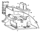
- FIG. 1 shows a side view in partial cross-section of the vacuum deposition chamber, interface vessel and X-ray head according to one embodiment of the invention
- FIG. 2 shows a top view of the system according to FIG. 1 ;
- FIG. 3 shows a perspective view of the vacuum interface assembly according to the invention
- FIG. 4 is a top view of the vacuum interface assembly according to FIG. 3 ;
- FIG. 5 is a perspective view of the X-ray port according to the invention.
- FIG. 6 is a cross-sectional view along lines VI-VI of FIG. 5 ;
- FIG. 7 is a cross-sectional view of the system shown in FIG. 1 ;
- FIG. 8 is an enlarged view of box VIII from FIG. 7 ;
- FIG. 9 is a perspective view of the system showing a static X-ray head.
- FIG. 10 is a perspective view of the system showing a linear X-ray head.
- FIGS. 1 and 2 show a vacuum deposition chamber 10 in which a substrate is unwound from a roll 14 for inspection by an X-ray metrology machine 20 .
- Metrology machine 20 is mounted in a vacuum interface assembly 30 , which is mounted through a hole in vacuum deposition chamber 10 , and sealed to maintain the vacuum within chamber 10 . This sealing can be done via an O-ring or by any known method.
- vacuum interface assembly 30 comprises a housing 31 surrounded by an upper flange 32 .
- the housing can be configured to fit metrology machines of different sizes and can be used for a static mounted machine or a linear machine, as described below with regard to FIGS. 9 and 10 .
- At the bottom of housing 31 is an X-ray port 35 .
- X-ray port 35 is a steel cylinder through which two apertures 36 , 37 extend, as shown in FIGS. 5 and 6 .
- aperture 36 extends through port 35 perpendicular to the plane of port 35 .
- Aperture 37 extends at an angle other than 90 degrees to the plane of the port. Covering each of apertures 36 , 37 is a beryllium window 38 , 39 , respectively. Beryllium windows 38 , 39 allow X-rays to pass through to and from substrate 12 while protecting X-ray metrology machine 20 and maintaining the vacuum inside chamber 10 .
- X-ray metrology machine 20 with X-ray generator 25 is mounted within vacuum interface assembly 30 , and extends into the cavity of vacuum chamber 10 .
- Vacuum interface assembly 30 is positioned so that X-rays from generator 25 can reach substrate 12 as it is unrolled from roll 14 .
- the bottom of machine 20 is preferably positioned approximately 0.5 inches above the substrate 12 , to allow for accurate measurements.
- FIG. 8 shows a detail of the X-ray metrology machine 20 in operation.
- X-rays 27 generated from generator 25 pass through aperture 36 to substrate 12 .
- the X-rays 29 fluorescing off of substrate 12 then pass upward through aperture 37 to reach detector 28 .
- Information from detector 28 is then sent to a control station 40 (see FIGS. 9 and 10 ) for analysis of the substrate.
- the beryllium windows covering apertures 36 and 37 ensure that infrared radiation from the substrate does not affect the measurements of X-ray metrology machine 10 , and yet allows X-rays to penetrate to reach substrate 12 .
- FIGS. 9 and 10 show two different ways the vacuum interface assembly can function.
- vacuum interface assembly 30 is structured to fit closely around metrology machine 20 , which remains fixed during analysis of substrate 12 . However, as shown in FIG. 10 , for larger substrates, a linearly movable arrangement is preferable, so that the entire width of the substrate can be tested.
- vacuum interface assembly 60 is wider than X-ray metrology machine 20 .
- Machine 20 is mounted in vacuum interface assembly 60 so that it can move along the width of interface 60 and take measurements in several different locations along the width of substrate 12 .
- Several of X-ray ports 35 can be mounted in the bottom of vacuum interface assembly 60 to allow for the several different measurements.
Landscapes
- Physics & Mathematics (AREA)
- Health & Medical Sciences (AREA)
- Life Sciences & Earth Sciences (AREA)
- Chemical & Material Sciences (AREA)
- Analytical Chemistry (AREA)
- Biochemistry (AREA)
- General Health & Medical Sciences (AREA)
- General Physics & Mathematics (AREA)
- Immunology (AREA)
- Pathology (AREA)
- Analysing Materials By The Use Of Radiation (AREA)
Abstract
Description
Claims (12)
Priority Applications (1)
| Application Number | Priority Date | Filing Date | Title |
|---|---|---|---|
| US12/925,361 US8340244B1 (en) | 2009-10-21 | 2010-10-20 | Vacuum interface assembly |
Applications Claiming Priority (2)
| Application Number | Priority Date | Filing Date | Title |
|---|---|---|---|
| US27943409P | 2009-10-21 | 2009-10-21 | |
| US12/925,361 US8340244B1 (en) | 2009-10-21 | 2010-10-20 | Vacuum interface assembly |
Publications (1)
| Publication Number | Publication Date |
|---|---|
| US8340244B1 true US8340244B1 (en) | 2012-12-25 |
Family
ID=47359729
Family Applications (1)
| Application Number | Title | Priority Date | Filing Date |
|---|---|---|---|
| US12/925,361 Expired - Fee Related US8340244B1 (en) | 2009-10-21 | 2010-10-20 | Vacuum interface assembly |
Country Status (1)
| Country | Link |
|---|---|
| US (1) | US8340244B1 (en) |
-
2010
- 2010-10-20 US US12/925,361 patent/US8340244B1/en not_active Expired - Fee Related
Similar Documents
| Publication | Publication Date | Title |
|---|---|---|
| US10770324B2 (en) | Substrate holding device, substrate transport device, processing arrangement and method for processing a substrate | |
| Fonoll-Rubio et al. | Insights into interface and bulk defects in a high efficiency kesterite-based device | |
| US8927051B2 (en) | Method for manufacturing a compound film | |
| KR101248561B1 (en) | Detection device and inspection device | |
| CN101689578B (en) | Photovoltaic modules and energy or light generating modules | |
| US20090308431A1 (en) | Concentrator photovoltaic device; photovoltaic unit for use therein and manufacturing method for this | |
| TWI458967B (en) | Electron beam device | |
| Clark et al. | The use of nuclear reactions and SIMS for quantitative depth profiling of hydrogen in amorphous silicon | |
| US20210036174A1 (en) | Durable solar panels | |
| KR101119459B1 (en) | Photoelectric conversion device and method for manufacturing the same | |
| Probst et al. | New developments in Cu (In, Ga)(S, Se) 2 thin film modules formed by rapid thermal processing of stacked elemental layers | |
| EP2283523B1 (en) | Assembly line for photovoltaic devices | |
| CA2707466A1 (en) | Conformal protective coating for solar panel | |
| US20140159752A1 (en) | Rapid analysis of buffer layer thickness for thin film solar cells | |
| EP1607769A1 (en) | Scintillator panel, scintillator panel laminate, radiation image sensor using the same, and radiation energy discriminator | |
| JP2013520565A (en) | Arrays, systems, and methods for processing multilayer bodies | |
| US8340244B1 (en) | Vacuum interface assembly | |
| JP2011082202A (en) | Inspection device | |
| KR20210129660A (en) | Apparatus, equipment and method for heat treatment of laminates | |
| EP1401007B1 (en) | An electron diffraction system for use in production environment and for high pressure deposition techniques | |
| KR101584467B1 (en) | Method and device for the industrial wiring and final testing of photovoltaic concentrator modules | |
| CN219475454U (en) | A sample surface analysis device | |
| US20120135561A1 (en) | Photoelectric-conversion-device fabrication method | |
| CN104475972B (en) | The efficient crystal silicon battery laser process equipment of a kind of solar energy back of the body passivation | |
| US11953631B2 (en) | Scintillator panel, and radiation detector |
Legal Events
| Date | Code | Title | Description |
|---|---|---|---|
| AS | Assignment |
Owner name: PRECISION FLOW TECHNOLOGIES, INC., NEW YORK Free format text: ASSIGNMENT OF ASSIGNORS INTEREST;ASSIGNOR:REILLY, FRANCIS;REEL/FRAME:025840/0269 Effective date: 20110211 |
|
| AS | Assignment |
Owner name: CERES TECHNOLOGIES, INC., NEW YORK Free format text: ASSIGNMENT OF ASSIGNORS INTEREST;ASSIGNOR:PRECISION FLOW TECHNOLOGIES, INC.;REEL/FRAME:028124/0486 Effective date: 20120417 |
|
| STCF | Information on status: patent grant |
Free format text: PATENTED CASE |
|
| REMI | Maintenance fee reminder mailed | ||
| AS | Assignment |
Owner name: AMETEK, INC., NEW JERSEY Free format text: ASSIGNMENT OF ASSIGNORS INTEREST;ASSIGNOR:CERES TECHNOLOGIES, INC.;REEL/FRAME:039471/0494 Effective date: 20160817 |
|
| FPAY | Fee payment |
Year of fee payment: 4 |
|
| SULP | Surcharge for late payment | ||
| FEPP | Fee payment procedure |
Free format text: MAINTENANCE FEE REMINDER MAILED (ORIGINAL EVENT CODE: REM.); ENTITY STATUS OF PATENT OWNER: SMALL ENTITY |
|
| LAPS | Lapse for failure to pay maintenance fees |
Free format text: PATENT EXPIRED FOR FAILURE TO PAY MAINTENANCE FEES (ORIGINAL EVENT CODE: EXP.); ENTITY STATUS OF PATENT OWNER: SMALL ENTITY |
|
| STCH | Information on status: patent discontinuation |
Free format text: PATENT EXPIRED DUE TO NONPAYMENT OF MAINTENANCE FEES UNDER 37 CFR 1.362 |
|
| FP | Lapsed due to failure to pay maintenance fee |
Effective date: 20201225 |