US8338555B2 - Photopolymers and their use in organic thin film transistors - Google Patents
Photopolymers and their use in organic thin film transistors Download PDFInfo
- Publication number
- US8338555B2 US8338555B2 US13/183,083 US201113183083A US8338555B2 US 8338555 B2 US8338555 B2 US 8338555B2 US 201113183083 A US201113183083 A US 201113183083A US 8338555 B2 US8338555 B2 US 8338555B2
- Authority
- US
- United States
- Prior art keywords
- group
- thin film
- organic thin
- dielectric
- present teachings
- Prior art date
- Legal status (The legal status is an assumption and is not a legal conclusion. Google has not performed a legal analysis and makes no representation as to the accuracy of the status listed.)
- Active
Links
- 0 [1*]/C(*C)=C(/[2*])C(=O)*C(C)(C)C Chemical compound [1*]/C(*C)=C(/[2*])C(=O)*C(C)(C)C 0.000 description 13
- ATIYCCSOPPETKD-UHFFFAOYSA-N *.*.*.C.C.CCCCC.CCCCC Chemical compound *.*.*.C.C.CCCCC.CCCCC ATIYCCSOPPETKD-UHFFFAOYSA-N 0.000 description 1
- ACYYOQGCNPIUKD-NOYJBFSESA-N C.CCC(C)(CCCC(C)(C)C(=O)OCCOC(=O)/C=C/C1=CC(C(F)(F)F)=CC=C1)C(=O)OCCOC(C)=O.CCC(C)(CCCC(C)(C)C(=O)OCCOC(=O)/C=C/C1=CC=CC=C1)C(=O)OCCOC(=O)C(F)(F)F.CCC(C)(CCCC(C)(C)C(=O)OCCOC(=O)/C=C/C1=CC=CC=C1)C(=O)OCCOC(=O)C1=C(F)C(C)=C(F)C(F)=C1F.CCC(C)(CCCC(C)(C)C(=O)OCCOC(=O)/C=C/C1=CC=CC=C1)C(=O)OCCOC(C)=O Chemical compound C.CCC(C)(CCCC(C)(C)C(=O)OCCOC(=O)/C=C/C1=CC(C(F)(F)F)=CC=C1)C(=O)OCCOC(C)=O.CCC(C)(CCCC(C)(C)C(=O)OCCOC(=O)/C=C/C1=CC=CC=C1)C(=O)OCCOC(=O)C(F)(F)F.CCC(C)(CCCC(C)(C)C(=O)OCCOC(=O)/C=C/C1=CC=CC=C1)C(=O)OCCOC(=O)C1=C(F)C(C)=C(F)C(F)=C1F.CCC(C)(CCCC(C)(C)C(=O)OCCOC(=O)/C=C/C1=CC=CC=C1)C(=O)OCCOC(C)=O ACYYOQGCNPIUKD-NOYJBFSESA-N 0.000 description 1
- PRCXERLGGHENFM-QPYPNWQTSA-N CCC(C)(C)C(=O)OCCOC(=O)/C(F)=C(\F)C1=CC=CC=C1.CCC(C)(C)C(=O)OCCOC(=O)/C(F)=C/C1=CC=CC=C1.CCC(C)(C)C(=O)OCCOC(=O)/C=C(\F)C1=CC=CC=C1.CCC(C)(C)C(=O)OCCOC(=O)/C=C/C1=CC=CC=C1.CCC(C)(CC(C)C1=CC=C(OC(=O)/C=C/C2=CC=CC=C2)C=C1)C(=O)OC.CCC(C)C1=CC=C(OC(=O)/C=C/C2=CC=CC=C2)C=C1 Chemical compound CCC(C)(C)C(=O)OCCOC(=O)/C(F)=C(\F)C1=CC=CC=C1.CCC(C)(C)C(=O)OCCOC(=O)/C(F)=C/C1=CC=CC=C1.CCC(C)(C)C(=O)OCCOC(=O)/C=C(\F)C1=CC=CC=C1.CCC(C)(C)C(=O)OCCOC(=O)/C=C/C1=CC=CC=C1.CCC(C)(CC(C)C1=CC=C(OC(=O)/C=C/C2=CC=CC=C2)C=C1)C(=O)OC.CCC(C)C1=CC=C(OC(=O)/C=C/C2=CC=CC=C2)C=C1 PRCXERLGGHENFM-QPYPNWQTSA-N 0.000 description 1
- HRYPIZBZUFQZDV-DIAHXYGKSA-N CCC(C)(C)C(=O)OCCOC(=O)/C=C/C1=CC=C(C)C=C1.CCC(C)(C)C(=O)OCCOC(=O)/C=C/C1=CC=C(C)C=C1.CCC(C)(C)C(=O)OCCOC(=O)/C=C/C1=CC=C(C)C=C1.CCC(C)(C)C(=O)OCCOC(=O)/C=C/C1=CC=C(C)C=C1.CCC(C)(C)C(=O)OCCOC(=O)/C=C/C1=CC=C(C)C=C1 Chemical compound CCC(C)(C)C(=O)OCCOC(=O)/C=C/C1=CC=C(C)C=C1.CCC(C)(C)C(=O)OCCOC(=O)/C=C/C1=CC=C(C)C=C1.CCC(C)(C)C(=O)OCCOC(=O)/C=C/C1=CC=C(C)C=C1.CCC(C)(C)C(=O)OCCOC(=O)/C=C/C1=CC=C(C)C=C1.CCC(C)(C)C(=O)OCCOC(=O)/C=C/C1=CC=C(C)C=C1 HRYPIZBZUFQZDV-DIAHXYGKSA-N 0.000 description 1
- LLCCBUJNKXYLAM-XNQYDSFPSA-N CCC(C)(C)C(=O)OCCOC(=O)/C=C/C1=CC=C(C)C=C1.CCC(C)(C)C(=O)OCCOC(=O)/C=C/C1=CC=C(C)C=C1.CCC(C)(C)C(=O)OCCOC(=O)/C=C/C1=CC=C(C)C=C1.CCC(C)(C)C(=O)OCCOC(=O)/C=C/C1=CC=CC(C(F)(F)F)=C1.CCC(C)(C)C(=O)OCCOC(=O)/C=C/C1=CC=CC=C1 Chemical compound CCC(C)(C)C(=O)OCCOC(=O)/C=C/C1=CC=C(C)C=C1.CCC(C)(C)C(=O)OCCOC(=O)/C=C/C1=CC=C(C)C=C1.CCC(C)(C)C(=O)OCCOC(=O)/C=C/C1=CC=C(C)C=C1.CCC(C)(C)C(=O)OCCOC(=O)/C=C/C1=CC=CC(C(F)(F)F)=C1.CCC(C)(C)C(=O)OCCOC(=O)/C=C/C1=CC=CC=C1 LLCCBUJNKXYLAM-XNQYDSFPSA-N 0.000 description 1
- XHAYAFIHEJMNDF-IJCAQYQPSA-N CCC(C)(CC(C)(C)C(=O)OCCOC(=O)/C(F)=C(\F)C1=CC=CC=C1)C(=O)OCCOC(C)=O.CCC(C)(CC(C)(C)C(=O)OCCOC(=O)/C(F)=C/C1=CC=CC=C1)C(=O)OCCOC(C)=O.CCC(C)(CC(C)(C)C(=O)OCCOC(=O)/C=C(\F)C1=CC=CC=C1)C(=O)OCCOC(C)=O.CCC(C)(CC(C)(C)C(=O)OCCOC(=O)/C=C/C1=CC=CC(C(F)(F)F)=C1)C(=O)OCCOC(C)=O.CCC(C)(CC(C)(C)C(=O)OCCOC(=O)/C=C/C1=CC=CC=C1)C(=O)OCCOC(=O)C1=C(F)C(F)=C(F)C(F)=C1F Chemical compound CCC(C)(CC(C)(C)C(=O)OCCOC(=O)/C(F)=C(\F)C1=CC=CC=C1)C(=O)OCCOC(C)=O.CCC(C)(CC(C)(C)C(=O)OCCOC(=O)/C(F)=C/C1=CC=CC=C1)C(=O)OCCOC(C)=O.CCC(C)(CC(C)(C)C(=O)OCCOC(=O)/C=C(\F)C1=CC=CC=C1)C(=O)OCCOC(C)=O.CCC(C)(CC(C)(C)C(=O)OCCOC(=O)/C=C/C1=CC=CC(C(F)(F)F)=C1)C(=O)OCCOC(C)=O.CCC(C)(CC(C)(C)C(=O)OCCOC(=O)/C=C/C1=CC=CC=C1)C(=O)OCCOC(=O)C1=C(F)C(F)=C(F)C(F)=C1F XHAYAFIHEJMNDF-IJCAQYQPSA-N 0.000 description 1
- HUXUKRAOCMMVKI-QIZKAFIGSA-N CCC(C)(CC(C)(C)C(=O)OCCOC(=O)/C=C/C1=CC=CC=C1)C(=O)OCCOC(=O)C(F)(F)F.CCC(C)(CC(C)(C)C(=O)OCCOC(=O)/C=C/C1=CC=CC=C1)C(=O)OCCOC(C)=O.CCC(C)(CC(C)(C)C(=O)OCCOC(=O)/C=C/C1=CC=CC=C1)C(=O)OCCOC(C)=O.CCC(C)(CC(C)(C)C(=O)OCCOC(=O)/C=C/C1=CC=CC=C1)C(=O)OCCOC(C)=O.CCC(C)(CC(CC(C)C1=CC=C(O)C=C1)C1=CC=C(OC(=O)/C=C/C2=CC=CC=C2)C=C1)C(=O)OC Chemical compound CCC(C)(CC(C)(C)C(=O)OCCOC(=O)/C=C/C1=CC=CC=C1)C(=O)OCCOC(=O)C(F)(F)F.CCC(C)(CC(C)(C)C(=O)OCCOC(=O)/C=C/C1=CC=CC=C1)C(=O)OCCOC(C)=O.CCC(C)(CC(C)(C)C(=O)OCCOC(=O)/C=C/C1=CC=CC=C1)C(=O)OCCOC(C)=O.CCC(C)(CC(C)(C)C(=O)OCCOC(=O)/C=C/C1=CC=CC=C1)C(=O)OCCOC(C)=O.CCC(C)(CC(CC(C)C1=CC=C(O)C=C1)C1=CC=C(OC(=O)/C=C/C2=CC=CC=C2)C=C1)C(=O)OC HUXUKRAOCMMVKI-QIZKAFIGSA-N 0.000 description 1
- MOYGJODVKHOXLC-KHBAIMJNSA-N COC(=O)C(C)(C)CCC(C)C1=CC=C(OC(=O)/C=C/C2=CC=C(C)C=C2)C=C1.COC(=O)C(C)(C)CCC(C)C1=CC=C(OC(=O)/C=C/C2=CC=C(C)C=C2)C=C1.COC(=O)C(C)(C)CCC(C)C1=CC=C(OC(=O)/C=C/C2=CC=C(C)C=C2)C=C1 Chemical compound COC(=O)C(C)(C)CCC(C)C1=CC=C(OC(=O)/C=C/C2=CC=C(C)C=C2)C=C1.COC(=O)C(C)(C)CCC(C)C1=CC=C(OC(=O)/C=C/C2=CC=C(C)C=C2)C=C1.COC(=O)C(C)(C)CCC(C)C1=CC=C(OC(=O)/C=C/C2=CC=C(C)C=C2)C=C1 MOYGJODVKHOXLC-KHBAIMJNSA-N 0.000 description 1
- DVOLWZKASUNPRO-IQIDSAGHSA-N COC(=O)C(C)(C)CCC(C)C1=CC=C(OC(=O)/C=C/C2=CC=C(C)C=C2)C=C1.COC(=O)C(C)(C)CCC(C)C1=CC=C(OC(=O)/C=C/C2=CC=C(C)C=C2)C=C1.COC(=O)C(C)(C)CCC(C)C1=CC=C(OC(=O)/C=C/C2=CC=C(C)C=C2)C=C1.COC(=O)C(C)(C)CCC(C)C1=CC=C(OC(=O)/C=C/C2=CC=C(C)C=C2)C=C1.COC(=O)C(C)(C)CCC(C)C1=CC=C(OC(=O)/C=C/C2=CC=C(C)C=C2)C=C1 Chemical compound COC(=O)C(C)(C)CCC(C)C1=CC=C(OC(=O)/C=C/C2=CC=C(C)C=C2)C=C1.COC(=O)C(C)(C)CCC(C)C1=CC=C(OC(=O)/C=C/C2=CC=C(C)C=C2)C=C1.COC(=O)C(C)(C)CCC(C)C1=CC=C(OC(=O)/C=C/C2=CC=C(C)C=C2)C=C1.COC(=O)C(C)(C)CCC(C)C1=CC=C(OC(=O)/C=C/C2=CC=C(C)C=C2)C=C1.COC(=O)C(C)(C)CCC(C)C1=CC=C(OC(=O)/C=C/C2=CC=C(C)C=C2)C=C1 DVOLWZKASUNPRO-IQIDSAGHSA-N 0.000 description 1
- GFFGUFNVIJTYFR-PEPPOZDASA-N [3H]1C=CC2=C1C=CC=C2.[3H]1C=CC2=C1C=CC=N2.[3H]1C=CC2=C1C=CN=C2.[3H]1C=CC2=C1C=NC=C2.[3H]1C=CC2=C1N=CC=C2.[3H]1C=CC=C1.[3H]1C=CC=N1.[3H]1C=CN=C1.[3H]1C=CN=N1.[3H]1C=NC2=C1C=CC=C2.[3H]1C=NC2=C1C=CC=N2.[3H]1C=NC2=C1C=CN=C2.[3H]1C=NC2=C1C=NC=C2.[3H]1C=NC2=C1N=CC=C2.[3H]1C=NC=N1.[3H]1C=NN=C1.[3H]1C=NN=N1.[3H]1N=CC2=C1C=CC=C2.[3H]1N=CC2=C1C=CC=N2.[3H]1N=CC2=C1C=CN=C2.[3H]1N=CC2=C1C=NC=C2.[3H]1N=CC2=C1N=CC=C2.[3H]1N=CC=N1 Chemical compound [3H]1C=CC2=C1C=CC=C2.[3H]1C=CC2=C1C=CC=N2.[3H]1C=CC2=C1C=CN=C2.[3H]1C=CC2=C1C=NC=C2.[3H]1C=CC2=C1N=CC=C2.[3H]1C=CC=C1.[3H]1C=CC=N1.[3H]1C=CN=C1.[3H]1C=CN=N1.[3H]1C=NC2=C1C=CC=C2.[3H]1C=NC2=C1C=CC=N2.[3H]1C=NC2=C1C=CN=C2.[3H]1C=NC2=C1C=NC=C2.[3H]1C=NC2=C1N=CC=C2.[3H]1C=NC=N1.[3H]1C=NN=C1.[3H]1C=NN=N1.[3H]1N=CC2=C1C=CC=C2.[3H]1N=CC2=C1C=CC=N2.[3H]1N=CC2=C1C=CN=C2.[3H]1N=CC2=C1C=NC=C2.[3H]1N=CC2=C1N=CC=C2.[3H]1N=CC=N1 GFFGUFNVIJTYFR-PEPPOZDASA-N 0.000 description 1
Images


Classifications
-
- C—CHEMISTRY; METALLURGY
- C08—ORGANIC MACROMOLECULAR COMPOUNDS; THEIR PREPARATION OR CHEMICAL WORKING-UP; COMPOSITIONS BASED THEREON
- C08F—MACROMOLECULAR COMPOUNDS OBTAINED BY REACTIONS ONLY INVOLVING CARBON-TO-CARBON UNSATURATED BONDS
- C08F220/00—Copolymers of compounds having one or more unsaturated aliphatic radicals, each having only one carbon-to-carbon double bond, and only one being terminated by only one carboxyl radical or a salt, anhydride ester, amide, imide or nitrile thereof
- C08F220/02—Monocarboxylic acids having less than ten carbon atoms; Derivatives thereof
- C08F220/10—Esters
Definitions
- OTFTs organic thin-film transistors
- RFID radiofrequency identification
- crosslinkable polymeric dielectrics such as crosslinked melamine/Cr 6+ salts-polyvinylphenol (PVP) and crosslinked benzocyclobutene (BCB) have been introduced.
- PVP polyvinylphenol
- BCB crosslinked benzocyclobutene
- these polymer films require high annealing temperatures and their leakage current densities are usually higher than 10 ⁇ 7 A/cm 2 at 2 MV/cm.
- the high current leakage densities of these polymeric dielectrics are believed to be due to, among other factors, the hydrophilic nature of phenol-based polymers and the presence of crosslinker additives.
- polymers with a hydrophobic backbone such as poly(methylmethacrylate) (PMMA) and polystyrene offer the possibility of achieving much lower TFT gate leakage current densities and greater environmental stability.
- PMMA poly(methylmethacrylate)
- polystyrene offer the possibility of achieving much lower TFT gate leakage current densities and greater environmental stability.
- These hydrophobic polymers are often soluble in common organic solvents but, because of the lack of crosslinking functionality, they cannot withstand subsequent solution-phase processing steps in which additional layers are deposited.
- crosslinkable polymeric dielectric materials that can exhibit low current leakage densities, that can be prepared via solution processes, that can be air- and/or moisture-stable, and that can be compatible with diverse gate and/or semiconductor materials.
- the present teachings provide photopolymer-based dielectric materials (e.g. films) and associated devices that can address various deficiencies and shortcomings of the prior art, including those outlined above.
- the present teachings provide photopolymers that can be used to prepare dielectric materials.
- polymers of the present teachings can be soluble in common organic solvents but can become insoluble in the same solvents after undergoing crosslinking, for example, photocrosslinking, which gives rise to certain processing advantages.
- the present teachings provide polymers having crosslinkable functional groups, for example, photocrosslinkable functional groups, that allow the polymers to crosslink.
- the crosslinking functionality can allow formation of a densely crosslinked polymeric matrix.
- Photopolymers of the present teachings and their crosslinked products can have excellent insulating properties, which enable their use as dielectrics.
- the photopolymers and their crosslinked products can have a leakage current density that is less than or equals to about 1 ⁇ 10 ⁇ 8 A/cm 2 at 2 MV/cm.
- Polymers of the present teachings can have a pendant group having the formula:
- R 1 , R 2 , R 3 , R 4 , R 5 , R 6 , R 7 , R 8 , L, L′, W, Z, m, and n are as defined herein.
- the present teachings also provide dielectric materials that include the polymers described above.
- the dielectric materials can be prepared from the polymers described above.
- Multilayer dielectric materials are provided which include two or more layers of dielectric materials sequentially deposited on top of each other, where at least one of the layers is prepared from polymers of the present teachings. These photopolymers can be used to prepare dielectric materials using various solution processes, including various printing techniques.
- the present teachings further provide electronic devices that include or are made from any of the dielectric materials described above.
- electronic devices include, but are not limited to, organic thin film transistors (OTFTs) (e.g., organic field effect transistors (OFETs)) and capacitors.
- OFTs organic thin film transistors
- these devices can include, for example, a substrate component, a semiconductor component, and/or a metallic contact component.
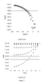
- FIG. 1 provides leakage current density (J) versus electric field (E) plots of various metal-insulator-semiconductor capacitor structures of different feature sizes in which the insulating layer is a dielectric material of the present teachings [P(CyVP 0.55 -co-MMA 0.45 )].
- FIG. 2 provides leakage current density (J) versus electric field (E) plots of various metal-insulator-semiconductor capacitor structures that were fabricated using dielectric materials of the present teachings and other comparative dielectric materials.
- FIG. 3 provides leakage current density (J) versus electric field (E) plots of various metal-insulator-semiconductor capacitor structures that were fabricated using dielectric materials of the present teachings and other comparative dielectric materials.
- FIG. 4 provides representative transfer and output plots of pentacene-based organic field effect transistors fabricated with spin-coated dielectric materials of the present teachings [P(CyEMA 0.57 -co-F5BEMA 0.43 )].
- FIG. 5 provides representative transfer and output plots of n-type organic field effect transistors fabricated with spin-coated dielectric materials of the present teachings [P(CyVP 0.55 -co-MMA 0.45 )].
- FIG. 6 provides a leakage current density (J) versus electric field (E) plot of a metal-insulator-semiconductor capacitor structure that incorporates a two-layer dielectric material of the present teachings [P(CyVP 0.55 -co-MMA 0.45 )].
- FIG. 7 provides representative transfer and output plots of a pentacene-based organic field effect transistor that incorporates a multilayer dielectric material of the present teachings [P(CyVP 0.55 -co-MMA 0.45 )].
- FIG. 8 provides representative transfer and output plots of pentacene-based organic field effect transistors fabricated with printed dielectric materials of the present teachings [P(CyEMA 0.80 -co-AcEMA 0.20 )].
- FIG. 9 shows an IR absorption spectrum of a dielectric material of the present teachings before and after crosslinking.
- FIG. 10 shows a typical DSC plot of a polymer of the present teachings.
- FIG. 11 shows a leakage current density (J) versus electric field (E) plot of a metal-insulator-semiconductor capacitor structure that incorporates a dielectric material of the present teachings having been stored in air for 55 days.
- FIG. 12 provides representative transfer and output plots of an organic field effect transistor that incorporates a printed dielectric material of the present teachings and a drop-cast semiconductor layer prepared from N,N′-bis(n-octyl)-dicyanoperylene-3,4:9,10-bis(dicarboximide) (PDI-8CN 2 ).
- FIG. 13 provides a leakage current density (J) versus electric field (E) plot of a metal-insulator-semiconductor capacitor structure that incorporates a dielectric material of the present teachings having a film thickness of 100 nm.
- FIG. 14 provides leakage current density (J) versus electric field (E) plots of various metal-insulator-semiconductor capacitor structures that were fabricated using a dielectric material of the present teachings [P(CyVP 0.55 -co-MMA 0.45 )] and a comparative dielectric material [P(VP 0.30 -co-CyVP 0.25 -co-MMA 0.45 )].
- FIG. 15 provides leakage current density (J) versus electric field (E) plots of metal-insulator-semiconductor capacitor structures that were fabricated using spin-coated dielectric materials of the present teachings (photopatterned and rinsed versus no photopatterning/rinsing).
- FIG. 16 illustrates different configurations of organic field effect transistors.
- FIG. 17 provides representative transfer and output plots of a bottom-contact bottom-gate organic field effect transistor that incorporates a spin-coated dielectric material of the present teachings and a vapor-deposited semiconductor layer prepared from pentacene.
- FIG. 18 provides a representative transfer plot of a bottom-contact top-gate organic field effect transistor that incorporates a spin-coated dielectric material of the present teachings and a vapor-deposited semiconductor layer prepared from pentacene.
- FIG. 19 provides a representative output plot of a top-contact bottom-gate organic field effect transistor that incorporates a spin-coated dielectric material of the present teachings and a conducting polymer as the bottom-gate electrode.
- the present teachings relate to photopolymers that can be used to prepare dielectric materials, the dielectric materials so prepared, methods for preparing the photopolymers and the dielectric materials, as well as to compositions, articles, structures, and devices that include such photopolymers and dielectric materials.
- the present teachings provide solution-processable polymers that can be crosslinked, for example, photocrosslinked, to provide insoluble robust dielectric materials that can exhibit excellent insulating properties and can be used to fabricate various organic electronic devices, including OTFTs.
- the dielectric materials also can be air-stable and have long shelf stability, and can be compatible with a wide range of p-type and n-type organic and inorganic semiconductors, making them attractive materials for fabricating various organic electronic devices.
- compositions are described as having, including, or comprising specific components, or where processes are described as having, including, or comprising specific process steps, it is contemplated that compositions of the present teachings also consist essentially of, or consist of, the recited components, and that the processes of the present teachings also consist essentially of, or consist of, the recited process steps.
- polymer or “polymeric compound” refers to a molecule consisting of at least two repeating units (monomers) connected by covalent chemical bonds.
- the polymer or polymeric compound can have only one type of repeating unit as well as two or more types of different repeating units. In the latter case, the term “copolymer” or “copolymeric compound” can be used instead, especially when the polymer includes chemically significantly different repeating units.
- a polymer typically comprises a backbone with optional pendant groups. Unless specified otherwise, the assembly of the repeating units in the copolymer can be head-to-tail, head-to-head, or tail-to-tail.
- the copolymer can be a random copolymer, an alternating copolymer, or a block copolymer.
- formulae similar to the ones below can be used to represent a copolymer, and such formula should be interpreted to embrace a copolymer having any repeating pattern consisting of x % of Q 1 , y % of Q 2 , and z % of Q 3 , where Q 1 , Q 2 , and Q 3 are different repeating units:
- a “pendant group” refers to a moiety that is substituted on the backbone of a polymer.
- photopolymer refers to a polymer that can be cured, for example, crosslinked, by exposure to light, often in the ultraviolet region of the spectrum, or other types of radiation.
- solution-processable refers to compounds, materials, or compositions that can be used in various solution-phase processes including, but not limited to, spin-coating, printing (e.g., inkjet printing), spray coating, electrospray coating, drop casting, dip coating, and blade coating.
- halo or “halogen” refers to fluoro, chloro, bromo, and iodo.
- amino refers to —NH 2 , an —NH-alkyl group, an —N(alkyl) 2 group, an —NH-arylalkyl group, an —N(alkyl)-arylalkyl group, and an —N(arylalkyl) 2 group, and is within the definition of —NR 1 R 2 , wherein R 1 and R 2 are as defined herein.
- alkoxy refers to —O-alkyl group, and is within the definition of —OR 3 , wherein R 3 is as defined herein.
- alkoxy groups include, but are not limited to, methoxy, ethoxy, propoxy (e.g., n-propoxy and isopropoxy), t-butoxy groups, and the like.
- alkylthio refers to an —S-alkyl group.
- alkylthio groups include, but are not limited to, methylthio, ethylthio, propylthio (e.g., n-propylthio and isopropylthio), t-butylthio groups, and the like.
- esters refers to both an —O—C(O)-alkyl group and a —C(O)—O-alkyl group, where the former group is within the definition of —OC(O)R 3 , and R 3 is as defined herein.
- oxo refers to a double-bonded oxygen (i.e., ⁇ O).
- alkyl refers to a straight-chain or branched saturated hydrocarbon group.
- alkyl groups include methyl (Me), ethyl (Et), propyl (e.g., n-propyl and isopropyl), butyl (e.g., n-butyl, isobutyl, sec-butyl, tert-butyl), pentyl groups (e.g., n-pentyl, isopentyl, neopentyl), and the like.
- an alkyl group can have 1 to 30 carbon atoms, i.e., a C 1-30 alkyl group, and, for example, an alkyl group can have 1 to 20 carbon atoms, i.e., a C 1-20 alkyl group. In some embodiments, an alkyl group can have 1 to 6 carbon atoms, and can be referred to as a “lower alkyl group.” Examples of lower alkyl groups include methyl, ethyl, propyl (e.g., n-propyl and isopropyl), and butyl groups (e.g., n-butyl, isobutyl, sec-butyl, tert-butyl). In some embodiments, alkyl groups can be substituted as disclosed herein.
- haloalkyl refers to an alkyl group having one or more halogen substituents.
- haloalkyl groups include, but are not limited to, CF 3 , C 2 F 5 , CHF 2 , CH 2 F, CCl 3 , CHCl 2 , CH 2 Cl, C 2 Cl 5 , and the like.
- Perhaloalkyl groups i.e., alkyl groups wherein all of the hydrogen atoms are replaced with halogen atoms (e.g., CF 3 and C 2 F 5 ), are included within the definition of “haloalkyl.”
- a C 1-20 haloalkyl group can have the formula —C n X 2n+1 or —C n H 2n+1-t X t , wherein X is F, Cl, Br, or I, n is an integer in the range of 1 to 20, and t is an integer in the range of 0 to 41, provided that t is less than or equal to 2n+1.
- alkenyl refers to a straight-chain or branched alkyl group having one or more carbon-carbon double bonds.
- alkenyl groups include, but are not limited to, ethenyl, propenyl, butenyl, pentenyl, hexenyl, butadienyl, pentadienyl, hexadienyl groups, and the like.
- the one or more carbon-carbon double bonds can be internal (such as in 2-butene) or terminal (such as in 1-butene).
- an alkenyl group can have 2 to 20 carbon atoms, i.e., a C 2-20 alkenyl group.
- alkenyl groups can be substituted as disclosed herein.
- alkynyl refers to a straight-chain or branched alkyl group having one or more triple carbon-carbon bonds.
- alkynyl groups include, but are not limited to, ethynyl, propynyl, butynyl, pentynyl, and the like.
- the one or more triple carbon-carbon bonds can be internal (such as in 2-butyne) or terminal (such as in 1-butyne).
- an alkynyl group can have 2 to 20 carbon atoms, i.e., a C 2-20 alkynyl group.
- alkynyl groups can be substituted as disclosed herein.
- cycloalkyl refers to a non-aromatic carbocyclic group including cyclized alkyl, alkenyl, and alkynyl groups.
- a cycloalkyl group can be monocyclic (e.g., cyclohexyl) or polycyclic (e.g., containing fused, bridged, and/or spiro ring systems), wherein the carbon atoms are located inside or outside of the ring system. Any suitable ring position of the cycloalkyl group can be covalently linked to the defined chemical structure.
- cycloalkyl groups include, but are not limited to, cyclopropyl, cyclobutyl, cyclopentyl, cyclohexyl, cycloheptyl, cyclopentenyl, cyclohexenyl, cyclohexadienyl, cycloheptatrienyl, norbornyl, norpinyl, norcaryl, adamantyl, and spiro[4.5]decanyl groups, as well as their homologs, isomers, and the like.
- a cycloalkyl group can have 3 to 14 carbon atoms, including 3 to 10 carbon atoms (i.e., a C 3-10 cycloalkyl group). In some embodiments, cycloalkyl groups can be substituted as disclosed herein.
- heteroatom refers to an atom of any element other than carbon or hydrogen and includes, for example, nitrogen, oxygen, silicon, sulfur, phosphorus, and selenium.
- cycloheteroalkyl refers to a non-aromatic cycloalkyl group that contains at least one ring heteroatom selected from O, N, and S, and optionally contains one or more double or triple bonds.
- a cycloheteroalkyl group can have 3 to 20 ring atoms, including 3 to 14 ring atoms (i.e., a 3-14 membered cycloheteroalkyl group).
- One or more N or S atoms in a cycloheteroalkyl ring may be oxidized (e.g., morpholine N-oxide, thiomorpholine S-oxide, thiomorpholine S,S-dioxide).
- nitrogen atoms of cycloheteroalkyl groups can bear a substituent, for example, a hydrogen atom, an alkyl group, or other substituents as described herein.
- Cycloheteroalkyl groups can also contain one or more oxo groups, such as oxopiperidyl, oxooxazolidyl, dioxo-(1H,3H)-pyrimidyl, oxo-2(1H)-pyridyl, and the like.
- cycloheteroalkyl groups include, among others, morpholinyl, thiomorpholinyl, pyranyl, imidazolidinyl, imidazolinyl, oxazolidinyl, pyrazolidinyl, pyrazolinyl, pyrrolidinyl, pyrrolinyl, tetrahydrofuranyl, tetrahydrothiophenyl, piperidinyl, piperazinyl, and the like.
- cycloheteroalkyl groups can be substituted as disclosed herein.
- aryl refers to an aromatic monocyclic hydrocarbon ring system or a polycyclic ring system in which two or more aromatic hydrocarbon rings are fused (i.e., having a bond in common with) together or at least one aromatic monocyclic hydrocarbon ring is fused to one or more cycloalkyl and/or cycloheteroalkyl rings.
- An aryl group can have from 6 to 14 carbon atoms in its ring system, which can include multiple fused rings.
- a polycyclic aryl group can have from 7 to 14 carbon atoms. Any suitable ring position of the aryl group can be covalently linked to the defined chemical structure.
- aryl groups having only aromatic carbocyclic ring(s) include, but are not limited to, phenyl, 1-naphthyl (bicyclic), 2-naphthyl (bicyclic), anthracenyl (tricyclic), phenanthrenyl (tricyclic), and like groups.
- polycyclic ring systems in which at least one aromatic carbocyclic ring is fused to one or more cycloalkyl and/or cycloheteroalkyl rings include, among others, benzo derivatives of cyclopentane (i.e., an indanyl group, which is a 5,6-bicyclic cycloalkyl/aromatic ring system), cyclohexane (i.e., a tetrahydronaphthyl group, which is a 6,6-bicyclic cycloalkyl/aromatic ring system), imidazoline (i.e., a benzimidazolinyl group, which is a 5,6-bicyclic cycloheteroalkyl/aromatic ring system), and pyran (i.e., a chromenyl group, which is a 6,6-bicyclic cycloheteroalkyl/aromatic ring system).
- aryl groups include, but are not limited to, benzodioxanyl, benzodioxolyl, chromanyl, indolinyl groups, and the like.
- aryl groups can be substituted with up to five substitution groups as disclosed herein.
- an aryl group can be substituted with one to five halogen substituents and such an aryl group can be referred to as a “haloaryl” group.
- a haloaryl group is a perhalophenyl group, where the phenyl group is substituted with five halogen atoms.
- heteroaryl refers to an aromatic monocyclic ring system containing at least 1 ring heteroatom selected from oxygen (O), nitrogen (N), and sulfur (S) or a polycyclic ring system where at least one of the rings present in the ring system is aromatic and contains at least 1 ring heteroatom.
- Polycyclic heteroaryl groups include two or more heteroaryl rings fused together and monocyclic heteroaryl rings fused to one or more aromatic carbocyclic rings (aryl groups), non-aromatic carbocyclic rings (cycloalkyl groups), and/or non-aromatic cycloheteroalkyl groups.
- a heteroaryl group as a whole, can have, for example, from 5 to 14 ring atoms and contain 1-5 ring heteroatoms.
- the heteroaryl group can be attached to the defined chemical structure at any heteroatom or carbon atom that results in a stable structure.
- heteroaryl rings do not contain O—O, S—S, or S—O bonds.
- one or more N or S atoms in a heteroaryl group can be oxidized (e.g., pyridine N-oxide, thiophene S-oxide, thiophene S,S-dioxide).
- heteroaryl groups include, for example, the 5-membered monocyclic and 5-6 bicyclic ring systems shown below:
- T is O, S, NH, N-alkyl, N-aryl, or N-(arylalkyl) (e.g., N-benzyl).
- heteroaryl groups include pyrrolyl, furyl, thienyl, pyridyl, pyrimidyl, pyridazinyl, pyrazinyl, triazolyl, tetrazolyl, pyrazolyl, imidazolyl, isothiazolyl, thiazolyl, thiadiazolyl, isoxazolyl, oxazolyl, oxadiazolyl, indolyl, isoindolyl, benzofuryl, benzothienyl, quinolyl, 2-methylquinolyl, isoquinolyl, quinoxalyl, quinazolyl, benzotriazolyl, benzimidazolyl, benzothiazolyl, benzisothiazolyl, benzisoxazo
- heteroaryl groups include, but are not limited to, 4,5,6,7-tetrahydroindolyl, tetrahydroquinolyl, benzothienopyridyl, benzofuropyridyl, and the like. In some embodiments, heteroaryl groups can be substituted as disclosed herein.
- compounds of the present teachings can include a “divalent group” defined herein as a linking group capable of forming a covalent bond with two other moieties.
- compounds of the present teachings can include, but are not limited to, a divalent C 1-20 alkyl group such as a methylene group.
- LG refers to a charged or uncharged atom (or group of atoms) that can be displaced as a stable species as a result of, for example, a substitution or elimination reaction.
- leaving groups include, but are not limited to, halide (e.g., Cl, Br, I), tosylate (toluenesulfonyl group, TsO), mesylate (methanesulfonyl group, MsO), brosylate (p-bromobenzenesulfonyl group, BsO), nosylate (4-nitrobenzenesulfonyl group, NsO), water (H 2 O), ammonia (NH 3 ), and triflate (trifluoromethanesulfonyl group, OTf).
- halide e.g., Cl, Br, I
- tosylate toluenesulfonyl group, TsO
- mesylate methanesulfonyl group,
- C 1-6 alkyl is specifically intended to individually disclose C 1 , C 2 , C 3 , C 4 , C 5 , C 6 , C 1 -C 6 , C 1 -C 5 , C 1 -C 4 , C 1 -C 3 , C 1 -C 2 , C 2 -C 6 , C 2 -C 5 , C 2 -C 4 , C 2 -C 3 , C 3 -C 6 , C 3 -C 5 , C 3 -C 4 , C 4 -C 6 , C 4 -C 5 , and C 5 -C 6 alkyl.
- an integer in the range of 0 to 40 is specifically intended to individually disclose 0, 1, 2, 3, 4, 5, 6, 7, 8, 9, 10, 11, 12, 13, 14, 15, 16, 17, 18, 19, 20, 21, 22, 23, 24, 25, 26, 27, 28, 29, 30, 31, 32, 33, 34, 35, 36, 37, 38, 39, and 40, and an integer in the range of 1 to 20 is specifically intended to individually disclose 1, 2, 3, 4, 5, 6, 7, 8, 9, 10, 11, 12, 13, 14, 15, 16, 17, 18, 19, and 20.
- the present teachings provide photopolymers that include one or more crosslinkable functionalities.
- the crosslinking group can form or be a portion of a pendant group covalently attached to the backbone of the polymers. More specifically, the present teachings provide a polymer including a pendant group having the formula:
- L at each occurrence, is independently —Y, —Y—O—Y—, -Q-, —Y—S—Y—, —Y—C(O)—O—Y—, -Q-C(O)—O—Y—, —Y—O—C(O)-Q-, —Y—O—C(O)—Y—, -Q-C(O)-Q-, —Y—C(O)—Y—, -Q-C(O)—Y—, or —Y—C(O)-Q-;
- Q at each occurrence, is —O—[Y—O] p —Y—O—;
- Y at each occurrence, is a divalent C 1-10 alkyl group, a divalent C 2-10 alkenyl group, a divalent C 2-10 alkynyl group, a divalent C 6-10 aryl group, or a covalent bond, wherein each of the C 1-10 alkyl group, the C 2-10 alkenyl group, the C 2-10 alkynyl group, and the C 6-10 aryl group is optionally substituted with 1 to 5 substituents independently selected from a halogen and CN; and
- p is an integer in the range of 0 to 10;
- R 1 and R 2 are independently H, a halogen, or CN;
- Z is a C 1-10 alkyl group, a C 1-10 haloalkyl group, or a C 6-10 aryl group optionally substituted with 1 to 5 substituents independently selected from a halogen, CN, a C 1-20 alkyl group,
- a C 1-20 haloalkyl group a C 1-20 alkoxy group, a —O—C 1-20 haloalkyl group, a —C(O)—C 1-6 alkyl group, a —C(O)—C 1-6 haloalkyl group, and a —C(O)—O—C 1-6 alkyl group.
- R 1 and R 2 can be independently H or F.
- Z can be a C 1-6 alkyl group, a C 1-6 perfluoroalkyl group, or a phenyl group optionally substituted with 1 to 5 substituents independently selected from a halogen such as F, a C 1-20 alkyl group, a C 1-20 haloalkyl group, a C 1-20 alkoxy group, and a —O—C 1-20 haloalkyl group.
- Z can be a phenyl group, a perhalophenyl group, or a phenyl group substituted with a trifluoromethyl group, a C 1-20 alkoxy group, or a —O—C 1-20 haloalkyl group.
- L at each occurrence, can be independently —O—, —C 6 H 5 —O—, —C(O)—O—, —C(O)—O—CH 2 CH 2 —O—, —C(O)—O—CF 2 CF 2 —O—, or a covalent bond.
- polymers of the present teachings can have a repeating unit having the formula:
- R 3 , R 4 , and R 5 are independently H, a halogen, a C 1-10 alkyl group, or a C 6-14 aryl group, wherein each of the C 1-10 alkyl group and the C 6-14 aryl group is optionally substituted with 1 to 5 substituents independently selected from a halogen and CN; and R 1 , R 2 , L, and Z are as defined herein.
- polymers of the present teachings can have a repeating unit having a formula selected from:
- polymers of the present teachings can have a repeating unit having the formula:
- U is —Y— or —Y—O—Y—;
- R 12 is H, a C 1-20 alkyl group, or a C 1-20 haloalkyl group; and
- Y is as defined herein.
- U can be —O— or a covalent bond.
- R 12 can be H, —CF 3 , a hexyl group, a decyl group, an octadecyl group, or —(CH 2 ) 3 (CF 2 ) 7 CF 3 .
- polymers of the present teachings can have a repeating unit selected from:
- polymers of the present teachings can have the formula:
- R 6 , R 7 , and R 8 are independently H, a halogen, a C 1-10 alkyl group, or a C 6-14 aryl group, wherein each of the C 1-10 alkyl group and the C 6-14 aryl group is optionally substituted with 1 to 5 substituents independently selected from a halogen and CN;
- L′ is —Y—, —Y—O—Y—, -Q-, —Y—S—Y—, —Y—C(O)—O—Y—, -Q-C(O)—O—Y—, —Y—O—C(O)-Q-, —Y—O—C(O)—Y—, -Q-C(O)-Q-, —Y—C(O)—Y—, -Q-C(O)-Q-, —Y—C(O)—Y—, -Q-C(O)—Y—, or —Y—C(O)-Q-;
- the polymers can have the formula:
- R 1 , R 2 , R 3 , R 6 , W, Z, m, and n are as defined herein.
- the polymers can have a formula selected from:
- the polymer can have the formula:
- the polymer can have a formula selected from:
- the polymer can have the formula:
- R 9 , R 10 , and R 11 are independently H, a halogen, a C 1-10 alkyl group, or a C 6-14 aryl group, wherein each of the C 1-10 alkyl group and the C 6-14 aryl group is optionally substituted with 1 to 5 substituents independently selected from a halogen and CN;
- W′ is a C 1-10 alkyl group, a C 1-10 haloalkyl group, a C 1-10 alkoxy group, or a C 6-10 aryl group optionally substituted with 1 to 5 substituents independently selected from a halogen, CN, a C 1-6 alkyl group, a C 1-6 haloalkyl group, a C 1-6 alkoxy group, a —C(O)—C 1-6 alkyl group, a —C(O)—C 1-6 haloalkyl group, and a —C(O)—O—C 1-6 alkyl group;
- W′ can be a C 1-6 alkyl group, a C 1-6 haloalkyl group, or a C 6-10 aryl group optionally substituted with 1 to 5 substituents independently selected from a halogen, CN, a C 1-6 alkyl group, a C 1-6 haloalkyl group, a C 1-6 alkoxy group, a —C(O)—C 1-6 alkyl group, a —C(O)—C 1-6 haloalkyl group, and a —C(O)—O—C 1-6 alkyl group.
- W′ can be a C 1-6 alkyl group or a C 1-6 haloalkyl group.
- W′ can be CF 3 .
- Polymers of the present teachings can include, but are not limited to, the polymers below:
- Photopolymers of the present teachings can be synthesized following Scheme 1 below.
- the desired pendant group can be coupled to a polymer, for example, a hydrophobic polymeric backbone, by reacting nucleophilic groups on the polymer with an acyl chloride, an acyl anhydride, or similar derivatives and groups that can form covalent bonds with nucleophilic groups, for example, electrophilic groups.
- a polymer for example, a hydrophobic polymeric backbone
- nucleophilic groups on the polymer for example, an acyl chloride, an acyl anhydride, or similar derivatives and groups that can form covalent bonds with nucleophilic groups, for example, electrophilic groups.
- the polymers disclosed herein can have satisfactory solubility in common organic solvents.
- common organic solvents include, but are not limited to, petroleum ethers; aromatic hydrocarbons such as benzene, chlorobenzene, dichlorobenzene, cyclohexylbenzene, toluene, xylene, and mesitylene; ketones such as acetone, 2-butanone, and cyclohexanone; ethers such as tetrahydrofuran, diethyl ether, bis(2-methoxyethyl)ether, and dioxane; alcohols such as ethanol, propanol, and isopropyl alcohol; aliphatic hydrocarbons, such as hexanes; acetates, such as ethyl acetate; halogenated aliphatic hydrocarbons such as dichloromethane, chloroform, and ethylene chloride; and other aprotic solvents such as dimethyl formamide and n-methyl pyr
- Polymers of the present teachings can be used in various solution-phase processes including, but not limited to, spin-coating, printing, drop casting, dip coating, spraying, and blade coating.
- Spin-coating involves applying an excess amount of the coating solution onto a substrate, then rotating the substrate at high speed to spread the fluid by centrifugal force.
- the thickness of the resulting dielectric film prepared by this technique is dependent on the spin-coating rate, the concentration of the solution, as well as the solvent used.
- Printing can be performed, for example, with a rotogravure printing press, a flexo printing press, or an inkjet printer. The thickness of the dielectric film in these cases will similarly be dependent on the concentration of the solution, the choice of solvent, and the number of printing repetitions.
- Ambient conditions such as temperature, pressure, and humidity, can also affect the resulting thickness of the film.
- printing quality can be affected by different parameters including, but not limited to, rheological properties of the inks such as solubility and viscosity.
- solubility For noncontact printing techniques such as inkjet printing, the solubility requirement is generally less stringent and a solubility range as low as about 1-4 mg/mL can suffice.
- a higher solubility range may be necessary, often in the range of about 50-100 mg/mL.
- Other contact printing techniques such as screen-printing and flexo printing, can require even higher solubility ranges, for example, about 100-1000 mg/mL.
- the crosslinking functionality allows formation of a densely crosslinked polymeric matrix.
- the crosslinked polymeric matrix is robust enough to withstand various conditions that are common in device fabrication processes, including patterning and subsequent solution-phase processes, for example, to form/deposit overlying layers (e.g., the semiconductor layer in a top-contact OFET).
- the crosslinking chemistry can include a 2+2 photo-stimulated cycloaddition that provides stable cyclobutane moieties.
- the crosslinking chemistry can also involve free radical additions.
- Polymers of the present teachings can be cured, for example, photocrosslinked, by exposure to ultraviolet light at, for example, a wavelength of about 245 nm to 350 nm. Crosslinking can also be achieved by other types of radiation, for example, with ion beams of charged particles, and with radioactive sources. Subsequent to the formation of the crosslinked matrix, the dielectric material of the present teachings can be subject to further patterning and process steps, by which additional layers, including additional dielectric, semiconductor and/or conducting layers, can be formed on top of the dielectric material.
- Photopolymers of the present teachings can be used to prepare dielectric materials that can exhibit a wide range of desirable properties and characteristics including, but not limited to, low leakage current densities, high breakdown voltages, low hysteresis, large capacitance, uniform film thickness, solution-processability, fabricability at low temperatures and/or atmospheric pressures, air and moisture stability, and/or compatibility with diverse gate materials and/or semiconductors.
- Leakage current density is typically defined as a vector whose magnitude is the leakage current per cross-sectional area.
- leakage current refers to uncontrolled (“parasitic”) current flowing across region(s) of a semiconductor structure or device in which no current should be flowing, for example, current flowing across the gate oxide in a metal-oxide-semiconductor (MOS) structure.
- MOS metal-oxide-semiconductor
- the leakage current density of a dielectric material can be determined by fabricating a standard metal-insulator-semiconductor (MIS) and/or metal-insulator-metal (MIM) capacitor structures with the dielectric material, then measuring the leakage current, and dividing the measured current by the area of the metal electrodes.
- MIS metal-insulator-semiconductor
- MIM metal-insulator-metal
- Photopolymers of the present teachings and their crosslinked products can have very low leakage current densities as measured from standard MIS and MIM capacitor structures.
- photopolymers of the present teachings and their crosslinked products can have a leakage current density of less than or equal to about 4 ⁇ 10 ⁇ 8 A/cm 2 at 2 MV/cm, less than or equal to about 2 ⁇ 10 ⁇ 8 A/cm 2 at 2 MV/cm, less than or equal to about 1 ⁇ 10 ⁇ 8 A/cm 2 at 2 MV/cm, less than or equal to about 8 ⁇ 10 ⁇ 9 A/cm 2 at 2 MV/cm, less than or equal to about 7 ⁇ 10 ⁇ 9 A/cm 2 at 2 MV/cm, less than or equal to about 6 ⁇ 10 ⁇ 9 A/cm 2 at 2 MV/cm, less than or equal to about 4 ⁇ 10 ⁇ 9 A/cm 2 at 2 MV/cm, less than or equal to about 2 ⁇ 10 ⁇ 9 A/cm 2 at
- Photopolymers of the present teachings also exhibit low leakage current densities at higher voltages, for example, a leakage current density of less than or equal to about 1 ⁇ 10 ⁇ 6 A/cm 2 at 4 MV/cm, less than or equal to about 5 ⁇ 10 ⁇ 7 A/cm 2 at 4 MV/cm, less than or equal to about 3 ⁇ 10 ⁇ 7 A/cm 2 at 4 MV/cm, less than or equal to about 1 ⁇ 10 ⁇ 7 A/cm 2 at 4 MV/cm, less than or equal to about 5 ⁇ 10 ⁇ 8 A/cm 2 at 4 MV/cm, or less than or equal to about 1 ⁇ 10 ⁇ 8 A/cm 2 at 4 MV/cm.
- Dielectric materials prepared from photopolymers of the present teachings also were found to be able to withstand very high breakdown voltages (i.e., the maximum voltage difference that can be applied across the dielectric before it breaks down and begins to conduct).
- dielectric materials of the present teachings can withstand a breakdown voltage of 4 MV/cm or higher, a breakdown voltage of 6 MV/cm or higher, or a breakdown voltage of 7 MV/cm or higher.
- Polymers of the present teachings also can have relatively low glass transition temperatures.
- polymers of the present teachings can have a glass transition temperature of less than about 100° C., a glass transition temperatures of less than about 90° C., a glass transition temperatures of less than about 80° C., a glass transition temperatures of less than about 70° C., a glass transition temperatures of less than about 60° C., a glass transition temperatures of less than about 50° C., a glass transition temperatures of less than about 40° C., or a glass transition temperatures of less than about 30° C.
- polymers of the present teachings can have a glass transition temperature in the range of about 30° C. to about 60° C.
- Glass transition temperature (T g ) can be defined as the mid-point of a temperature range at which a material gradually becomes more viscous and changes from a rubbery state to a glassy state. Due to this property, dielectric materials deposited from polymers of the present teachings can allow surface planarization and filling of pinholes before crosslinking, hence improving surface smoothness (for example, achieving a sub-nanometer surface roughness), and accordingly, device performance and operation. Pinholes can also be filled by depositing two or more layers of dielectric materials sequentially on top of one another, hence forming a multilayer dielectric material that can have very good surface uniformity and can be essentially pinhole-free over a large area.
- the present teachings further provide articles of manufacture, for example, composites, that includes a dielectric material of the present teachings and a substrate component and/or a semiconductor component.
- the substrate component can be selected from, but is not limited to, doped silicon, an indium tin oxide (ITO), ITO-coated glass, ITO-coated polyimide or other plastics, aluminum or other metals alone or coated on a polymer or other substrate, a doped polythiophene, and the like.
- the composite can include a semiconductor component.
- the semiconductor component can be selected from, but is not limited to, various fused heterocycles, polythiophenes, fused aromatics, and other such organic semiconductor compounds or materials, whether p-type or n-type, otherwise known or found useful in the art.
- the semiconductor component also can include inorganic semiconductor materials such as silicon, germanium, gallium arsenide, and the like.
- the composite can include one or more electrical contacts. Such electrical contacts can be made of a metal (e.g., gold) and can function as source, drain, or gate contacts.
- One or more of the composites described above can be embodied within various organic electronic devices such as OTFTs, specifically, OFETs, as well as capacitors, complementary circuits (e.g., inverter circuits), and the like.
- the method can include preparing a solution that includes the polymer described herein, and printing the solution onto a substrate to form a dielectric layer.
- the method can include exposing the dielectric layer to a radiation source (e.g., ultraviolet light) to induce crosslinking, thereby forming a crosslinked dielectric material.
- the method can also include printing an additional dielectric layer onto the crosslinked dielectric layer to form a multilayer dielectric material.
- Another aspect of the present teachings relates to methods for fabricating organic field effect transistors that include a dielectric material of the present teachings.
- the dielectric materials of the present teachings can be used to fabricate various types of organic field effect transistors including, but not limited to, top-gate top-contact capacitor structures, top-gate bottom-contact capacitor structures, bottom-gate top-contact capacitor structures, and bottom-gate bottom-contact capacitor structures.
- the method can include preparing a solution that includes the polymer described herein, printing the solution onto a substrate (gate) to form a dielectric layer, exposing the dielectric layer to radiation to induce crosslinking to form a crosslinked dielectric material, forming a semiconductor layer on the crosslinked dielectric material, and forming a first electrical contact and a second electrical contact (source and drain) on the semiconductor layer, to fabricate a top-contact bottom-gate organic field effect transistor.
- the method can include preparing a solution that includes one or more polymers described herein, printing the solution onto a substrate (gate) to form a dielectric layer, exposing the dielectric layer to radiation to induce crosslinking to form a crosslinked dielectric material, forming a first electrical contact and a second electrical contact (source and drain) on the crosslinked dielectric material, and forming a semiconductor layer above the first and second electrical contacts and the dielectric material (i.e., to cover the electrical contacts and an area of the dielectric material between the electrical contacts), to fabricate a bottom-contact bottom-gate organic field effect transistor.
- the method can include forming a first electrical contact and a second electrical contact (source and drain) on a substrate, forming a semiconductor layer above the substrate and the first and second electrical contacts (to cover the electrical contacts and an area of the substrate between the electrical contacts), preparing a solution that includes one or more polymers described herein, printing the solution onto the semiconductor layer to form a dielectric layer, exposing the dielectric layer to radiation to induce crosslinking to form a crosslinked dielectric material, forming a third electrical contact (gate) on the crosslinked dielectric material, wherein the third electrical contact is above an area between the first and second electrical contacts, to fabricate a bottom-contact top-gate organic field effect transistor.
- the method can include forming a semiconductor layer on a substrate, forming a first electrical contact and a second electrical contact (source and drain) on the semiconductor layer, preparing a solution that includes one or more polymers described herein, printing the solution onto the first and second electrical contacts and an area of the semiconductor layer between the first and second electrical contacts to form a dielectric layer, exposing the dielectric layer to radiation to induce crosslinking to form a crosslinked dielectric material, and forming a third electrical contact (gate) on the dielectric material, wherein the third electrical contact is above an area between the first and second electrical contacts, to fabricate a top-contact top-gate organic field effect transistor.
- the semiconductor layer and the various electrical contacts can be formed by various deposition processes known to those skilled in the art.
- the semiconductor layer can be formed by processes such as, but not limited to, physical vapor deposition, different types of printing techniques (e.g., flexo printing, litho printing, gravure printing, ink-jetting, pad printing, and so forth), drop casting, dip coating, doctor blading, roll coating, and spin-coating.
- Electrical contacts can be formed by processes such as, but not limited to, thermal evaporation and radiofrequency or e-beam sputtering, as well as various deposition processes, including but not limited to those described immediately above (e.g., flexo printing, litho printing, gravure printing, ink-jetting, pad printing, drop casting, dip coating, doctor blading, roll coating, and spin-coating).
- processes such as, but not limited to, thermal evaporation and radiofrequency or e-beam sputtering, as well as various deposition processes, including but not limited to those described immediately above (e.g., flexo printing, litho printing, gravure printing, ink-jetting, pad printing, drop casting, dip coating, doctor blading, roll coating, and spin-coating).
- polymers and dielectric materials according to the present teachings were prepared and characterized by NMR, IR spectroscopy, elemental analysis, differential scanning calorimetry (DSC), AFM, and metal-insulator-semiconductor (MIS) device leakage and impedance spectroscopy measurements, to demonstrate, among other things, their dielectric properties and their compatibility with various p-type and n-type organic semiconductors.
- Organic electronic devices for example, organic thin film transistors (OTFTs), specifically, organic field effect transistors (OFETs), based on these dielectric films also have been fabricated and characterized, data of which are provided below.
- PCyVP poly(vinylphenylcinnamate)
- PCyVP poly(vinylphenylcinnamate)
- P(CyEMA) poly(cinnamoylethylmethacrylate)
- the polymer precipitates were purified by repetitive precipitation to give about 2 g of a high molecular weight random copolymer poly(cinnamoylethyl methacrylate-co-acetoxyethyl methacrylate) [P(CyEMA 0.50 -co-AcEMA 0.50 )] as a white solid.
- 1 H NMR verified the copolymer ratio as 50%:50%.
- the polymer precipitates were purified by repetitive precipitation to give about 2 g of a random copolymer poly(cinnamoylethyl methacrylate-co-acetoxyethylmethacrylate) [P(CyEMA 0.57 -co-AcEMA 0.43 )] as a white solid.
- the polymer precipitates were purified by repetitive precipitation to give about 3 g of a random copolymer poly(cinnamoylethyl methacrylate-co-acetoxyethylmethacrylate) [P(CyEMA 0.80 -co-AcEMA 0.20 )] as a white solid.
- the polymer precipitates were purified by repetitive precipitation to give about 2 g of a random copolymer poly(cinnamoylethyl methacrylate-co-(trifluoroacetoxy)ethyl methacrylate) [P(CyEMA 0.57 -co-TFAcEMA 0.43 )] as a white solid.
- the polymer precipitates were purified by repetitive precipitation to give about 2 g of a random copolymer poly(cinnamoylethyl methacrylate-co-(pentafluorobenzoyl)ethylmethacrylate) [P(CyEMA 0.57 -co-F5BEMA 0.43 )] as a white solid.
- the polymer precipitates were purified by repetitive precipitation to give about 2 g of a random copolymer poly(3-(trifluoromethyl)-cinnamoylethylmethacrylate-co-acetoxyethyl methacrylate) [P(CF3CyEMA 0.57 -co-AcEMA 0.43 )] as a white solid.
- P(CyEMA) (3.0 g, Example 2) was dissolved in 30 mL of freshly distilled THF and the resulting solution was cooled into an ice-water bath.
- Trifluoroacetic anhydride (0.5 g) was added dropwise under vigorous stirring in the absence of light. The reaction was warmed to ambient temperature, stirred for 3 hours, and concentrated to dryness under reduced pressure. The resulted solid was dissolved in 30 mL freshly distilled THF and the resulting solution cooled in an ice-water bath. A second portion of trifluoroacetic anhydride (0.5 g) was added dropwise under vigorous stirring. The reaction was warmed to ambient temperature, stirred overnight, and concentrated under reduced pressure.
- the photopolymers from Examples 1-3 were dissolved in dioxane to give a solution having a concentration of 80 mg/mL, respectively.
- the polymer solutions were then spin-coated onto clean silicon substrates between 1300 rpm (acceleration 20). After the spin-coating step, the resulting dielectric films were treated in a 150 W ultraviolet oven for 10 minutes, and then annealed in a vacuum oven at 100° C. for 10 minutes to completely remove any residual solvent. Film thickness and surface smoothness (represented by root mean square (RMS) roughness) were determined by profilometry and atomic force microscopy (AFM), respectively. The results showed that the polymer films of the present teachings are very smooth, with RMS roughness being in the range of about 0.4 nm.
- RMS root mean square
- MIS capacitor structures were fabricated using the resulting dielectric films from Example 11, and capacitance of the dielectric films was measured.
- n-type Si MEMC Electronic Materials, Antimony/n-doped
- Using a shadow mask rectangular- or square-shaped Au pads having a feature size ranging from 100 ⁇ m ⁇ 100 ⁇ m to 1000 ⁇ m ⁇ 1000 ⁇ m, can be deposited to form MIS structures of different sizes.
- leakage currents in this and following examples were determined using capacitor structures with Au pads having a feature size of 200 ⁇ m ⁇ 200 ⁇ m.
- the J-E characteristics of capacitors based on the dielectric materials of the present teachings appear to be independent of the area of the Au pads, as shown in FIG. 1 .
- a triaxial cabling and probing system (Signatone, Gilroy, Calif.) was employed to probe the MIS structures. The combined use of the Signatone triaxial probing system and the Keithley 6430 source meter reduced the noise level to as low as 10 ⁇ 15 A and provided accurate current measurements as low as 10 ⁇ 14 A.
- the bottom electrode was probed with an instrument ground and the top Au pads were probed with a soft tip from the Triaxial probe connected to the Keithley source meter.
- an I-V scan was performed by applying bias to the traixial probe and measuring current through the circuit.
- the scan rate was between 5-15 s/step, which was controlled by setting the delay time to between 0.5 s and 2 s and the number of measurements per step between 10 and 20.
- J leakage current density
- E electric field
- Pentacene OFETs were fabricated with dielectric films from Examples 11 and 12 on both silicon and aluminium gate materials. Specifically, the silicon substrates were highly n-doped silicon wafers obtained from Montco Silicon Tech, Inc. (Spring City, Pa.) and cleaned by sonication in organic solvents before use. The aluminium substrates were cut from Al-coated plastic substrates. Pentacene was purchased from Sigma-Aldrich (St. Louis, Mo.) and vacuum-deposited at about 2 ⁇ 10 ⁇ 6 Torr (500 ⁇ , 0.3 ⁇ /s) while maintaining the substrate temperature at about 50° C. to about 70° C.
- Gold (Au) electrodes were vacuum-deposited through shadow masks at 3-4 ⁇ 10 ⁇ 6 Torr (500 ⁇ , 0.3 ⁇ /s). The channel length was 50 ⁇ m, and the channel width was 5000 ⁇ m. These OFETs were found to perform very well, with mobility ( ⁇ ) approximating 0.5 cm 2 /Vs, an I on :I off ratio up to 2 ⁇ 10 7 , negligible hysteresis, and extremely low gate leakage currents. Representative OFET transfer and output plots are shown in FIG. 4 (P(CyEMA 0.57 -co-F5BEMA 0.43 ) is used as the dielectric layer). OFET performances of these photopolymer-based devices are summarized in Table 2.
- a comparative pentacene OFET device was fabricated using silicon oxide (SiO 2 ) as the dielectric material.
- the silicon oxide film has a thickness of 300 nm.
- the carrier mobilities of this comparative device were found to be about 0.1 cm 2 /Vs to about 0.3 cm 2 /Vs.
- a perylene-type n-type semiconductor, N,N′-bis(n-octyl)-dicyanoperylene-3,4:9,10-bis(dicarboximide) (PDI-8CN 2 ) was used to fabricate n-type OFET devices with photopolymers of the present teachings as the dielectric layer.
- the silicon substrates were highly n-doped silicon wafers obtained from Montco Silicon Tech, Inc. (Spring City, Pa.) and cleaned by sonication in organic solvents before use.
- PDI-8CN 2 was synthesized according to procedures described in U.S. Patent Application Publication No.
- photopolymers of the present teachings are soluble in common organic solvents including, but not limited to, tetrahydrofuran, bis(2-methoxyethyl) ether, dioxane, chloroform, ethyl acetate, acetone, toluene, dichlorobenzene, cyclohexylbenzene, dimethylformamide, n-methyl pyrrolidone, and cyclohexanone.
- Photopolymers from Examples 1-10 have excellent solubility in common organic solvents.
- P(CyEMA) from Example 2 can be dissolved in ethyl acetate without heating to give a solution having a concentration of 350 mg/mL. Such a solution is sufficiently viscous for use in gravure printing.
- photopolymers of the present teachings can be cured by exposure to ultraviolet light (e.g., via treatment in a 150 W UV oven for 10 minutes), which renders them insoluble in the organic solvents in which they were initially soluble prior to the photocrosslinking step.
- the cured dielectric films were found to be robust enough to withstand relatively harsh processes. For example, a photocrosslinked dielectric film was sonicated in dichlorobenzene for 5 minutes, after which its thickness and physical appearance was found to be substantially the same as before the sonication step.
- photopolymers of the present teachings can become insoluble in common organic solvents after photocrosslinking, multiple layers of dielectric materials can be coated on top of one another without dissolving the earlier deposited layers.
- Such multilayer dielectric structures can offer many performance advantages including, but not limited to, minimized pinholes and better uniformity over larger areas.
- Example 3 The leakage current density (J) versus electric field (E) plot is shown in FIG. 6 . While the test pixel shown in FIG. 9 has a relatively large area of about 2 cm 2 (typical OFET devices and MIS structures have test pixels generally smaller than 0.01 cm 2 ), the leakage current density of the tested two-layer dielectric films is still extremely low, indicating excellent film uniformity over large areas.
- the thickness of the two-layer dielectric film was about 1000 nm, which is two times thicker than the single-layer films (500 nm) of Example 11, implicating the insolubility of the photocrosslinked film during the multilayer coating process.
- Pentacene OFETs were fabricated with the two-layer dielectric films described above. These pentacene OFETS exhibited excellent device performance, as evidenced by hole mobility ( ⁇ ) of about 0.22 cm 2 /Vs, I on :I off ratio of about 3 ⁇ 10 7 , negligible hysteresis, and gate leakage current as low as 3 nA at 180 V gate bias. The transfer and output plots are shown in FIG. 7 .
- Example 7 Using the photopolymer P(CyEMA 0.80 -co-AcEMA 0.20 ) of Example 7, printable dielectric layers were fabricated.
- the photopolymer was dissolved in ethyl acetate to give a solution having a concentration of 300 mg/mL solution.
- Dielectric films were printed using the printing press (IGT), using the gravure mode and the following parameters: Anilox force 100 N, printing speed 0.4 m/s, anilox cylinder 402.100 (40 l/cm, copper engraved-chromium plated, stylus 130°, screen angle 53, volume 23.3 mL/m 2 ).
- a first layer of the photopolymer was printed on Al-PEN substrate, UV cured for 10 minutes and dried in a vacuum oven for 10 minutes.
- a second layer of the photopolymer was printed onto the first layer and cured in the same way.
- MIS capacitor structures and pentacene OFETs were subsequently fabricated.
- the output and transfer plots of the pentacene OFETs are shown in FIG. 8 .
- Selected photopolymers of the present teachings were crosslinked by exposure to ultraviolet light at 254 nm. IR spectroscopy was used to confirm the photocrosslinking of these polymers.
- the double bond in the cinnamoyl group exhibited characteristic IR absorption at 1630 cm ⁇ 1 before photocrosslinking, and disappeared after the 2+2 cycloaddition photocrosslinking reaction as predicted.
- FIG. 9 shows the IR absorption spectrum for a photopolymer film before and after UV curing. It could be seen that the intensity of the C ⁇ O stretching is significantly reduced after the UV treatment.
- the glass transition properties of the present photopolymers were characterized by differential scanning calorimetry (DSC).
- FIG. 10 shows a typical DSC plot of photopolymers of the present teachings. Additional data for some of the photopolymers are summarized in Table 3.
- T g glass transition temperature of P(CyEMA 0.57 -co-AEMA 0.43 ) was measured to be about 45° C. (compared to conventional polymeric dielectric material such as PMMA, which has T g between 80-100° C.).
- Such low glass transition temperature allows a time period for achieving surface planarization and filling of pinholes before initiating the photocrosslinking step to obtain the final photocured crosslinked dielectric matrix, which can explain the good film forming properties of photopolymers of the present teachings.
- Polymers with lower glass transition temperatures e.g. PMMA, which has T g between about 80-100° C.
- PVP polymers with higher glass transition temperatures
- FIG. 11 shows the leakage current density versus electric field (J-E) plot of an MIS capacitor structure incorporating a dielectric film prepared from (P(CyVP 0.55 -co-MMA 0.45 ) that had been stored in air for 55 days. It can be seen that, despite the storage period, the photopolymer dielectric film still exhibited excellent dielectric properties, as evidenced by the very low the leakage current density (which actually decreased slightly after 55 days). These results therefore show that the present photopolymer materials possess excellent shelf stability as a dielectric material. As it is recognized, OH group-containing dielectric polymers are typically moisture-sensitive and have limited shelf stability.
- photopolymers of the present teachings have improved shelf stability compared to other known polymer dielectric materials such as PVP.
- Residual OH groups can be capped or masked, for example, by using suitable reagents, including trifluoroacetic anhydride (e.g., Example 11) or trifluoroacetyl chloride.
- a perylene-based n-type semiconductor, N,N′-bis(n-octyl)-dicyanoperylene-3,4:9,10-bis(dicarboximide) (PDI-8CN 2 ) was dropcasted from a dichlorobenzene solution (2 mg/mL) on a solution-deposited and then crosslinked photopolymer dielectric layer (700 nm) on a Si substrate. The substrate was maintained at 105° C., during which the solvent was evaporated to yield a crystalline semiconductor film. OFET devices were fabricated and tested using procedures similar to those described in the previous examples. Representative transfer and output plots are shown in FIG. 12 .
- N-type mobility was calculated to be as high as 0.035 cm 2 /Vs
- I on :I off ratio was measured to be about 1 ⁇ 10 4
- gate leakage current was measured to be less than or about 50 nA.
- FIG. 13 shows the J-E plot of a 100 nm thick photopolymer dielectric film.
- the data presented in FIG. 14 show comparable leakage current density compared to the 400 nm to 500 nm photopolymer dielectric films demonstrated in the earlier examples. It can be seen that the breakdown field of such a thin film can be as high as 7 MV/cm.
- the leakage current density vs electric field plots of P(CyVP 0.55 -co-MMA 0.45 ) (Example 3) and P(VP 0.30 -co-CyVP 0.25 -co-MMA 0.45 ) (Example 4) are compared in FIG. 14 . It can be seen that the leakage current density of P(CyVP 0.55 -co-MMA 0.45 ) is about two orders of magnitude lower that of P(VP 0.30 -co-CyVP 0.25 -co-MMA 0.45 ).
- a spincoated photopolymer film [P(CyEMA) in Example 2] was exposed to ultraviolet light (254 nm) through a shadow mask and then washed with THF and dried. The film exhibited a clear pattern negative to that of the shadow mask. Au electrodes were then evaporated on top of the exposed and crosslinked region of the film to fabricate an MIS capacitor structure, the leakage current of which was tested using similar procedures as described earlier.
- FIG. 15 shows the leakage current density vs electric field plot of such a dielectric film.
- the J-E response of a similar dielectric film without any photo patterning/solvent rinsing treatment also was shown in the figure for comparison. It can be seen that the leakage current of the patterned dielectric film was comparable to the unpatterned dielectric film.
- FIG. 16 illustrates the four common types of OFET structures: top-contact bottom-gate structure (a), bottom-contact bottom-gate structure (b), bottom-contact top-gate structure (c), and top-contact top-gate structure (d).
- an OFET can include a dielectric layer (e.g., shown as 8 , 8 ′, 8 ′′, and 8 ′′′ in FIGS. 16 a , 16 b , 16 c , and 16 d , respectively), a semiconductor layer (e.g., shown as 6 , 6 ′, 6 ′′, and 6 ′′′ in FIGS.
- a gate contact e.g., shown as 10 , 10 ′, 10 ′′, and 10 ′′′ in FIGS. 16 a , 16 b , 16 c , and 16 d , respectively
- a substrate e.g., shown as 12 , 12 ′, 12 ′′, and 12 ′′′ in FIGS. 16 a , 16 b , 16 c , and 16 d , respectively
- source and drain contacts e.g., shown as 2 , 2 ′, 2 ′′, 2 ′′′, 4 , 4 ′, 4 ′′, and 4 ′′′ in FIGS.
- bottom-contact bottom-gate OFETs were fabricated using a dielectric material of the present teachings [P(CyEMA) in Example 2] as the insulating layer.
- a dielectric film was fabricated on a Si substrate with a thickness of about 900 nm.
- Au 25 nm was evaporated onto the photopolymer film through a shadow mask to form source and drain electrodes, which were then treated in saturated alkylthiol ethanol solution for 1 hour.
- Pentacene 50 nm was then evaporated on top (the substrate temperature was 60° C.) to complete the bottom-contact device.
- the transfer and output plots of such a bottom-contact device are shown in FIG. 17 .
- Hole mobility of about 0.074 cm 2 /Vs and an I on /I off ratio of about 1 ⁇ 10 7 were obtained.
- bottom-contact top-gate OFETs were fabricated using a dielectric material of the present teachings [P(CyEMA) from Example 2] as the dielectric layer.
- Au 25 nm
- SiO 2 insulating substrate
- source and drain electrodes which were then treated in saturated alkylthiol ethanol solution for 1 hour.
- pentacene 50 nm
- Photopolymer films were then spin-coated on top of pentacene as the dielectric layer followed by deposition of Au as the gate electrode.
- the transfer plot of such a bottom-contact top-gate device is shown in FIG. 18 . Hole mobility of about 0.01 cm 2 /Vs and an I on /I off ratio of about 3 ⁇ 10 3 were obtained.
- top-contact OFETs were fabricated using a dielectric material of the present teachings [P(CyVP 0.55 -co-MMA 0.45 ) from Example 3] as the dielectric layer and a conducting polymer thin film as the bottom-gate electrode.
- a conducting polymer PEDOT-PSS, 1:1 ratio
- Dielectric and semiconductor layers n-type semiconductor, N,N′-bis(n-octyl)-dicyanonaphthalene-3,4:9,10-bis(dicarboximide), NDI-8CN 2 ) were then deposited using procedures similar to those described in Example 14.
Abstract
Description

wherein R1, R2, L, and Z are as defined herein. In certain embodiments, the present teachings provide polymers having the formula:

wherein R1, R2, R3, R4, R5, R6, R7, R8, L, L′, W, Z, m, and n are as defined herein.

where T is O, S, NH, N-alkyl, N-aryl, or N-(arylalkyl) (e.g., N-benzyl). Examples of heteroaryl groups include pyrrolyl, furyl, thienyl, pyridyl, pyrimidyl, pyridazinyl, pyrazinyl, triazolyl, tetrazolyl, pyrazolyl, imidazolyl, isothiazolyl, thiazolyl, thiadiazolyl, isoxazolyl, oxazolyl, oxadiazolyl, indolyl, isoindolyl, benzofuryl, benzothienyl, quinolyl, 2-methylquinolyl, isoquinolyl, quinoxalyl, quinazolyl, benzotriazolyl, benzimidazolyl, benzothiazolyl, benzisothiazolyl, benzisoxazolyl, benzoxadiazolyl, benzoxazolyl, cinnolinyl, 1H-indazolyl, 2H-indazolyl, indolizinyl, isobenzofuyl, naphthyridinyl, phthalazinyl, pteridinyl, purinyl, oxazolopyridinyl, thiazolopyridinyl, imidazopyridinyl, furopyridinyl, thienopyridinyl, pyridopyrimidinyl, pyridopyrazinyl, pyridopyridazinyl, thienothiazolyl, thienoxazolyl, thienoimidazolyl, and the like. Further examples of heteroaryl groups include, but are not limited to, 4,5,6,7-tetrahydroindolyl, tetrahydroquinolyl, benzothienopyridyl, benzofuropyridyl, and the like. In some embodiments, heteroaryl groups can be substituted as disclosed herein.

wherein:
L, at each occurrence, is independently —Y, —Y—O—Y—, -Q-, —Y—S—Y—, —Y—C(O)—O—Y—, -Q-C(O)—O—Y—, —Y—O—C(O)-Q-, —Y—O—C(O)—Y—, -Q-C(O)-Q-, —Y—C(O)—Y—, -Q-C(O)—Y—, or —Y—C(O)-Q-;

wherein:
R3, R4, and R5 are independently H, a halogen, a C1-10 alkyl group, or a C6-14 aryl group, wherein each of the C1-10 alkyl group and the C6-14 aryl group is optionally substituted with 1 to 5 substituents independently selected from a halogen and CN; and
R1, R2, L, and Z are as defined herein.

wherein R1, R2, R3, and Z are as defined herein. For example, polymers of the present teachings can have a repeating unit having the formula:

wherein:
U is —Y— or —Y—O—Y—;
R12 is H, a C1-20 alkyl group, or a C1-20 haloalkyl group; and
Y is as defined herein.


wherein:
R6, R7, and R8 are independently H, a halogen, a C1-10 alkyl group, or a C6-14 aryl group, wherein each of the C1-10 alkyl group and the C6-14 aryl group is optionally substituted with 1 to 5 substituents independently selected from a halogen and CN;
L′ is —Y—, —Y—O—Y—, -Q-, —Y—S—Y—, —Y—C(O)—O—Y—, -Q-C(O)—O—Y—, —Y—O—C(O)-Q-, —Y—O—C(O)—Y—, -Q-C(O)-Q-, —Y—C(O)—Y—, -Q-C(O)—Y—, or —Y—C(O)-Q-;
- W is a C1-10 alkyl group, a C1-10 haloalkyl group, a C1-10 alkoxy group, or a C6-10 aryl group optionally substituted with 1 to 5 substituents independently selected from a halogen, CN, a C1-6 alkyl group, a C1-6 haloalkyl group, a C1-6 alkoxy group, a —C(O)—C1-6 alkyl group, a —C(O)—C1-6 haloalkyl group, and a —C(O)—O—C1-6 alkyl group;
m and n are independently a real number, wherein 0<m≦1, 0≦n<1, and m+n=1; and R1, R2, R3, R4, R5, L, Q, Y, and Z are as defined herein.

wherein R1, R2, R3, R6, W, Z, m, and n are as defined herein.

wherein m and n are as defined herein.

wherein m, n, R12, and U are as defined herein.


wherein m and n are as defined herein.

wherein:
R9, R10, and R11 are independently H, a halogen, a C1-10 alkyl group, or a C6-14 aryl group, wherein each of the C1-10 alkyl group and the C6-14 aryl group is optionally substituted with 1 to 5 substituents independently selected from a halogen and CN;
W′ is a C1-10 alkyl group, a C1-10 haloalkyl group, a C1-10 alkoxy group, or a C6-10 aryl group optionally substituted with 1 to 5 substituents independently selected from a halogen, CN, a C1-6 alkyl group, a C1-6 haloalkyl group, a C1-6 alkoxy group, a —C(O)—C1-6 alkyl group, a —C(O)—C1-6 haloalkyl group, and a —C(O)—O—C1-6 alkyl group;
- m′, n′, and n″ are independently a real number, wherein 0<m′≦1, 0≦n′<1, 0≦n″<1, and m′+n′+n″=1; and
R1, R2, R3, R4, R5, R6, R7, R8, L, L′, W, and Z are as defined herein.


| TABLE 1 |
| Dielectric properties of different photopolymer-based dielectric films. |
| Leakage current | Leakage current | ||||
| density (A/cm2) | density (A/cm2) | Ci | Thickness | BV | |
| Photopolymer | at 2 MV/cm | at 4 MV/cm | (nF/cm2) | (nm) | (V) |
| P(CyVP0.55-co-MMA0.45) | 2 × 10⁻⁹ | 1 × 10⁻⁸ | 6.4 | 470 | >200 |
| CAP-P(CyVP0.55-co-MMA0.45) | 1 × 10⁻⁹ | 4 × 10⁻⁹ | 6.3 | 470 | >200 |
| P(CP0.3-co-CyVP0.25-co-MMA0.45) | 3 × 10⁻⁸ | 3 × 10⁻⁶ | 6.8 | 440 | >200 |
| P(CyEMA0.57-co-AcEMA0.43) | 2 × 10⁻⁹ | 6 × 10⁻⁸ | 7.1 | 410 | >200 |
| P(CyEMA0.8-co-AcEMA0.2) | 2 × 10⁻⁹ | 4 × 10⁻⁸ | 7.3 | 400 | >200 |
| P(CyEMA) | 2 × 10⁻⁹ | 1 × 10⁻⁸ | 6.0 | 460 | >200 |
| CAP-P(CyEMA) | 1 × 10⁻⁹ | 4 × 10⁻⁹ | 6.0 | 460 | >200 |
| P(CyEMA0.57-co-F5BEMA0.43) | 2 × 10⁻⁹ | 1 × 10⁻⁸ | 6.0 | 440 | >200 |
| P(CF3CyEMA0.57-co-AcEMA0.43) | 7 × 10⁻⁹ | 2 × 10⁻⁷ | 6.9 | 430 | >200 |
| P(CyEMA0.57-co-TFAcEMA0.43) | 6 × 10⁻⁹ | 3 × 10⁻⁷ | 6.9 | 480 | >200 |
| P(CyEMA0.5-co-AcEMA0.5) (High MW) | 4 × 10⁻⁹ | 4 × 10⁻⁸ | 7.8 | 400 | >200 |
| PVP | 6 × 10⁻⁷ | Break down | 6.5 | 570 | 150 V |
| PMMA | 7 × 10⁻⁹ | 1 × 10⁻⁷ | 12 | 250 | >200 |
| PCyVP | 2 × 10⁻⁸ | 1 × 10⁻⁶ | 9.5 | 300 | >200 |
| Crosslinkable polymer dielectrics | >1 × 10⁻⁷ | N/A | N/A | N/A | N/A |
| reported in the literature | |||||
| TABLE 2 |
| Pentacene field-effect transistor parameters for TFT devices |
| based on polymeric dielectric materials of the present teachings. |
| (*Carrier mobility was calculated in saturation.) |
| Gate | ||||
| Sub- | μ | leakage | ||
| Polymer # | strate | (cm2/Vs) | Ion:Ioff | (nA) |
| P(CyVP0.55-co-MMA0.45) | Si | 0.3 | 2 × 10⁶ | 10 |
| P(CP0.3-co-CyVP0.25-co-MMA0.45) | Si | 0.3 | 2 × 10⁶ | 100 |
| P(CyEMA0.57-co-AcEMA0.43) | Si | 0.8 | 1 × 10⁶ | 100 |
| P(CyEMA0.8-co-AcEMA0.2) | Si | 0.7 | 3 × 10⁶ | 40 |
| P(CyEMA) | Si | 1.0 | 2 × 10⁷ | 3 |
| CAP-P(CyEMA) | Si | 1.2 | 4 × 10⁷ | 2 |
| P(CyEMA0.57-co-F5BEMA0.43) | Si | 1.2 | 1 × 10⁷ | 1000 |
| P(CF3CyEMA0.57-co-AcEMA0.43) | Si | 0.3 | 5 × 10⁵ | 10 |
| P(CyEMA0.57-co-TFAcEMA0.43) | Si | 0.6 | 2 × 10⁶ | 20 |
| P(CyEMA0.8-co-AcEMA0.2) | Al | 0.32 | 1 × 10⁶ | 1 |
| PCyVP | Si | 0.65 | 1 × 10⁵ | 10000 |
| SiO2 | Si | 0.2 | 1 × 10⁶ | 10 |
| TABLE 3 |
| Glass transition temperatures. |
| Polymer | Tg (° C.) | ||
| Poly(vinyl phenol), |
150 | ||
| Poly(methylmethacrylate), PMMA | 80-100 | ||
| Poly(vinylphenylcinnamate), PCyVP (Example 1) | 100 | ||
| P(CyEMA) (Example 2) | 53 | ||
| P(CyEMA0.57-co-AcEMA0.43) (Example 6) | 45 | ||
| P(CyEMA0.57-co-F5BEMA0.43) (Example 9) | 56 | ||
| CAP-P(CyEMA) (Example 11) | 53 | ||
Claims (10)

Priority Applications (1)
| Application Number | Priority Date | Filing Date | Title |
|---|---|---|---|
| US13/183,083 US8338555B2 (en) | 2006-11-28 | 2011-07-14 | Photopolymers and their use in organic thin film transistors |
Applications Claiming Priority (3)
| Application Number | Priority Date | Filing Date | Title |
|---|---|---|---|
| US86130806P | 2006-11-28 | 2006-11-28 | |
| US11/998,159 US7981989B2 (en) | 2006-11-28 | 2007-11-28 | Photopolymer-based dielectric materials and methods of preparation and use thereof |
| US13/183,083 US8338555B2 (en) | 2006-11-28 | 2011-07-14 | Photopolymers and their use in organic thin film transistors |
Related Parent Applications (1)
| Application Number | Title | Priority Date | Filing Date |
|---|---|---|---|
| US11/998,159 Continuation US7981989B2 (en) | 2006-11-28 | 2007-11-28 | Photopolymer-based dielectric materials and methods of preparation and use thereof |
Publications (2)
| Publication Number | Publication Date |
|---|---|
| US20110266534A1 US20110266534A1 (en) | 2011-11-03 |
| US8338555B2 true US8338555B2 (en) | 2012-12-25 |
Family
ID=39311039
Family Applications (2)
| Application Number | Title | Priority Date | Filing Date |
|---|---|---|---|
| US11/998,159 Active 2029-05-03 US7981989B2 (en) | 2006-11-28 | 2007-11-28 | Photopolymer-based dielectric materials and methods of preparation and use thereof |
| US13/183,083 Active US8338555B2 (en) | 2006-11-28 | 2011-07-14 | Photopolymers and their use in organic thin film transistors |
Family Applications Before (1)
| Application Number | Title | Priority Date | Filing Date |
|---|---|---|---|
| US11/998,159 Active 2029-05-03 US7981989B2 (en) | 2006-11-28 | 2007-11-28 | Photopolymer-based dielectric materials and methods of preparation and use thereof |
Country Status (5)
| Country | Link |
|---|---|
| US (2) | US7981989B2 (en) |
| EP (1) | EP2089442B1 (en) |
| JP (1) | JP5148624B2 (en) |
| ES (1) | ES2525040T3 (en) |
| WO (1) | WO2008066826A1 (en) |
Cited By (5)
| Publication number | Priority date | Publication date | Assignee | Title |
|---|---|---|---|---|
| WO2015100333A1 (en) | 2013-12-24 | 2015-07-02 | Polyera Corporation | Support structures for an attachable, two-dimensional flexible electronic device |
| WO2016065276A1 (en) | 2014-10-24 | 2016-04-28 | Polyera Corporation | Photopatternable compositions and methods of fabricating transistor devices using same |
| US10254795B2 (en) | 2015-05-06 | 2019-04-09 | Flexterra, Inc. | Attachable, flexible display device with flexible tail |
| US10261634B2 (en) | 2014-03-27 | 2019-04-16 | Flexterra, Inc. | Infrared touch system for flexible displays |
| US10535325B2 (en) | 2014-05-28 | 2020-01-14 | Flexterra, Inc. | Low power display updates |
Families Citing this family (37)
| Publication number | Priority date | Publication date | Assignee | Title |
|---|---|---|---|---|
| US7605394B2 (en) | 2004-12-23 | 2009-10-20 | Northwestern University | Siloxane-polymer dielectric compositions and related organic field-effect transistors |
| US20070078675A1 (en) * | 2005-09-30 | 2007-04-05 | Kaplan Craig A | Contributor reputation-based message boards and forums |
| WO2008002660A2 (en) * | 2006-06-28 | 2008-01-03 | Northwestern University | Crosslinked polymeric dielectric materials and methods of manufacturing and use thereof |
| CN103560206B (en) * | 2008-11-24 | 2016-09-28 | 巴斯夫欧洲公司 | Photocurable polymeric dielectric and its production and use |
| US8592129B2 (en) * | 2009-08-31 | 2013-11-26 | Sumitomo Chemical Company, Limited | Resin, resist composition and method for producing resist pattern |
| TW201126606A (en) * | 2009-09-15 | 2011-08-01 | Sumitomo Chemical Co | Photocrosslinkable organic thin-film transistor insulation layer material |
| US8471253B2 (en) | 2010-05-19 | 2013-06-25 | Northwestern University | Crosslinked hybrid gate dielectric materials and electronic devices incorporating same |
| KR101841000B1 (en) | 2010-07-28 | 2018-03-22 | 스미또모 가가꾸 가부시키가이샤 | Photoresist composition |
| JP6195692B2 (en) | 2010-08-30 | 2017-09-13 | 住友化学株式会社 | RESIST COMPOSITION, METHOD FOR PRODUCING RESIST PATTERN, NOVEL COMPOUND AND RESIN |
| US8436068B2 (en) | 2010-10-27 | 2013-05-07 | Industrial Technology Research Institute | Composition and polymer |
| JP5829941B2 (en) * | 2011-02-25 | 2015-12-09 | 住友化学株式会社 | Resist composition and method for producing resist pattern |
| JP5829939B2 (en) | 2011-02-25 | 2015-12-09 | 住友化学株式会社 | Resist composition and method for producing resist pattern |
| JP5829940B2 (en) | 2011-02-25 | 2015-12-09 | 住友化学株式会社 | Resist composition and method for producing resist pattern |
| JP5947051B2 (en) | 2011-02-25 | 2016-07-06 | 住友化学株式会社 | Resist composition and method for producing resist pattern |
| JP5898520B2 (en) | 2011-02-25 | 2016-04-06 | 住友化学株式会社 | Resist composition and method for producing resist pattern |
| JP5898521B2 (en) | 2011-02-25 | 2016-04-06 | 住友化学株式会社 | Resist composition and method for producing resist pattern |
| JP5947053B2 (en) | 2011-02-25 | 2016-07-06 | 住友化学株式会社 | Resist composition and method for producing resist pattern |
| JP6034026B2 (en) | 2011-02-25 | 2016-11-30 | 住友化学株式会社 | Resist composition and method for producing resist pattern |
| JP6034025B2 (en) | 2011-02-25 | 2016-11-30 | 住友化学株式会社 | Resist composition and method for producing resist pattern |
| WO2012129511A2 (en) | 2011-03-24 | 2012-09-27 | Northwestern University | Semiconducting compounds and devices incorporating same |
| KR101308489B1 (en) | 2011-05-26 | 2013-09-17 | 경희대학교 산학협력단 | Liquid crystal alignment layers using poly(2-hydroxyalkyl methacrylate) derivatives and Method for preparation thereof |
| WO2012161106A1 (en) * | 2011-05-26 | 2012-11-29 | 住友化学株式会社 | Organic thin-film transistor insulating layer material |
| JP6013797B2 (en) | 2011-07-19 | 2016-10-25 | 住友化学株式会社 | Resist composition and method for producing resist pattern |
| JP5886696B2 (en) | 2011-07-19 | 2016-03-16 | 住友化学株式会社 | Resist composition and method for producing resist pattern |
| JP6013799B2 (en) | 2011-07-19 | 2016-10-25 | 住友化学株式会社 | Resist composition and method for producing resist pattern |
| JP5912912B2 (en) | 2011-07-19 | 2016-04-27 | 住友化学株式会社 | Resist composition and method for producing resist pattern |
| JP6189020B2 (en) | 2011-07-19 | 2017-08-30 | 住友化学株式会社 | Resist composition and method for producing resist pattern |
| US9171961B2 (en) * | 2012-07-11 | 2015-10-27 | Polyera Corporation | Coating materials for oxide thin film transistors |
| US9035287B2 (en) * | 2013-02-01 | 2015-05-19 | Polyera Corporation | Polymeric materials for use in metal-oxide-semiconductor field-effect transistors |
| CN105555822B (en) * | 2013-07-15 | 2018-05-08 | 飞利斯有限公司 | Can exposure image material and relevant electronic device and method |
| US9958778B2 (en) | 2014-02-07 | 2018-05-01 | Orthogonal, Inc. | Cross-linkable fluorinated photopolymer |
| JP6034326B2 (en) * | 2014-03-26 | 2016-11-30 | 富士フイルム株式会社 | Semiconductor device and composition for forming insulating layer |
| WO2016100983A1 (en) | 2014-12-19 | 2016-06-23 | Polyera Corporation | Photocrosslinkable compositions, patterned high k thin film dielectrics and related devices |
| US9761817B2 (en) | 2015-03-13 | 2017-09-12 | Corning Incorporated | Photo-patternable gate dielectrics for OFET |
| DE102015119939A1 (en) | 2015-11-18 | 2017-05-18 | ALTANA Aktiengesellschaft | Crosslinkable polymeric materials for dielectric layers in electronic components |
| DE102021125407A1 (en) | 2021-09-30 | 2023-03-30 | Polymer Competence Center Leoben Gmbh | Method of making a dielectric for a capacitor and Method of making a capacitor and capacitor |
| JP2023064968A (en) * | 2021-10-27 | 2023-05-12 | 東ソー株式会社 | Photo-crosslinkable polymer, insulation film, and organic electric field effect transistor device including the same |
Citations (21)
| Publication number | Priority date | Publication date | Assignee | Title |
|---|---|---|---|---|
| GB1517746A (en) | 1974-09-12 | 1978-07-12 | Fuji Photo Film Co Ltd | Method of producing a support for a printing plate |
| US5223356A (en) | 1990-08-24 | 1993-06-29 | University Of Lowell | Photocrosslinked second order nonlinear optical polymers |
| US5998101A (en) | 1997-04-25 | 1999-12-07 | Samsung Display Devices Co., Ltd. | Cinnamate-containing photopolymer for orientation film of liquid crystal display (LCD) and method of forming the orientation film using the photopolymer |
| US6258507B1 (en) | 1998-03-26 | 2001-07-10 | Sumitomo Chemical Company, Limited | Photoresist compositions |
| US6380271B1 (en) | 2000-04-07 | 2002-04-30 | Sumitomo Bakelite Company Limited | Material for electrical insulating organic film, electrical insulating organic film and process for the preparation thereof |
| US6458310B1 (en) | 1997-03-04 | 2002-10-01 | University Technologies International, Inc. | Process of making a polymeric material having a microporous matrix |
| US20040065929A1 (en) | 2002-09-28 | 2004-04-08 | Bon Won Koo | Organic gate insulating film and organic thin film transistor using the same |
| US20040211989A1 (en) | 2001-03-07 | 2004-10-28 | Marten Armgarth | Electrochemical device |
| US20040216641A1 (en) | 2002-11-13 | 2004-11-04 | Matsushita Electric Industrial Co., Ltd. | Composition for forming porous film, porous film and method for forming the same, interlevel insulator film, and semiconductor device |
| EP1494298A2 (en) | 2003-07-03 | 2005-01-05 | Samsung Electronics Co., Ltd. | Organic thin film transistor comprising multi-layered gate insulator |
| US20050019592A1 (en) | 2003-05-08 | 2005-01-27 | Feng Bai | Organic polymers, laminates, and capacitors |
| EP1541118A1 (en) | 2003-12-11 | 2005-06-15 | L'oreal | Hair cosmetic composition containing an elongated NANO-OBJECT from a cross-linked, synthetic polymer, process for applying this composition and uses |
| US20050176970A1 (en) | 2004-01-26 | 2005-08-11 | Marks Tobin J. | Perylene n-type semiconductors and related devices |
| US7029945B2 (en) | 2001-12-19 | 2006-04-18 | Merck Patent Gmbh | Organic field effect transistor with an organic dielectric |
| US20060186401A1 (en) | 2004-09-14 | 2006-08-24 | Marks Tobin J | Carbonyl-functionalized thiophene compounds and related device structures |
| US7098525B2 (en) | 2003-05-08 | 2006-08-29 | 3M Innovative Properties Company | Organic polymers, electronic devices, and methods |
| US20060202195A1 (en) | 2004-12-23 | 2006-09-14 | Marks Tobin J | Siloxane-polymer dielectric compositions and related organic field-effect transistors |
| US7270845B2 (en) | 2004-03-31 | 2007-09-18 | Endicott Interconnect Technologies, Inc. | Dielectric composition for forming dielectric layer for use in circuitized substrates |
| US20070282094A1 (en) | 2006-05-11 | 2007-12-06 | Marks Tobin J | Silole-based polymers and semiconductor materials prepared from the same |
| US20080021220A1 (en) | 2006-06-12 | 2008-01-24 | Marks Tobin J | Naphthalene-based semiconductor materials and methods of preparing and use thereof |
| US20080161464A1 (en) | 2006-06-28 | 2008-07-03 | Marks Tobin J | Crosslinked polymeric dielectric materials and methods of manufacturing and use thereof |
Family Cites Families (9)
| Publication number | Priority date | Publication date | Assignee | Title |
|---|---|---|---|---|
| JPS4940391A (en) * | 1972-08-28 | 1974-04-15 | ||
| JPS5027405B2 (en) * | 1973-05-18 | 1975-09-08 | ||
| JPS5037562B2 (en) * | 1973-08-01 | 1975-12-03 | ||
| JPS5540416A (en) * | 1978-09-14 | 1980-03-21 | Mitsubishi Chem Ind Ltd | Photosensitive composition |
| JPH0760265B2 (en) * | 1985-07-02 | 1995-06-28 | 三菱化学株式会社 | Photosensitive composition |
| JP2582089B2 (en) * | 1987-09-23 | 1997-02-19 | 千秋 東 | Photosensitive microgel ultrafine particles |
| EP0800563B1 (en) * | 1994-12-28 | 2000-07-12 | Cambridge Display Technology Limited | Polymers for use in optical devices |
| JP2005093921A (en) * | 2003-09-19 | 2005-04-07 | Canon Inc | Field effect organic transistor and manufacturing method thereof |
| JP4864375B2 (en) * | 2004-08-09 | 2012-02-01 | ドンジン セミケム カンパニー リミテッド | Photosensitive resin composition for spacer, spacer and liquid crystal display element |
-
2007
- 2007-11-28 ES ES07862266.9T patent/ES2525040T3/en active Active
- 2007-11-28 EP EP07862266.9A patent/EP2089442B1/en active Active
- 2007-11-28 US US11/998,159 patent/US7981989B2/en active Active
- 2007-11-28 WO PCT/US2007/024473 patent/WO2008066826A1/en active Application Filing
- 2007-11-28 JP JP2009539298A patent/JP5148624B2/en active Active
-
2011
- 2011-07-14 US US13/183,083 patent/US8338555B2/en active Active
Patent Citations (23)
| Publication number | Priority date | Publication date | Assignee | Title |
|---|---|---|---|---|
| GB1517746A (en) | 1974-09-12 | 1978-07-12 | Fuji Photo Film Co Ltd | Method of producing a support for a printing plate |
| US5223356A (en) | 1990-08-24 | 1993-06-29 | University Of Lowell | Photocrosslinked second order nonlinear optical polymers |
| US6458310B1 (en) | 1997-03-04 | 2002-10-01 | University Technologies International, Inc. | Process of making a polymeric material having a microporous matrix |
| US5998101A (en) | 1997-04-25 | 1999-12-07 | Samsung Display Devices Co., Ltd. | Cinnamate-containing photopolymer for orientation film of liquid crystal display (LCD) and method of forming the orientation film using the photopolymer |
| US6258507B1 (en) | 1998-03-26 | 2001-07-10 | Sumitomo Chemical Company, Limited | Photoresist compositions |
| US6380271B1 (en) | 2000-04-07 | 2002-04-30 | Sumitomo Bakelite Company Limited | Material for electrical insulating organic film, electrical insulating organic film and process for the preparation thereof |
| US20040211989A1 (en) | 2001-03-07 | 2004-10-28 | Marten Armgarth | Electrochemical device |
| US7029945B2 (en) | 2001-12-19 | 2006-04-18 | Merck Patent Gmbh | Organic field effect transistor with an organic dielectric |
| US20040065929A1 (en) | 2002-09-28 | 2004-04-08 | Bon Won Koo | Organic gate insulating film and organic thin film transistor using the same |
| US20040216641A1 (en) | 2002-11-13 | 2004-11-04 | Matsushita Electric Industrial Co., Ltd. | Composition for forming porous film, porous film and method for forming the same, interlevel insulator film, and semiconductor device |
| US7098525B2 (en) | 2003-05-08 | 2006-08-29 | 3M Innovative Properties Company | Organic polymers, electronic devices, and methods |
| US20050019592A1 (en) | 2003-05-08 | 2005-01-27 | Feng Bai | Organic polymers, laminates, and capacitors |
| US20050001210A1 (en) | 2003-07-03 | 2005-01-06 | Samsung Electronics Co., Ltd. | Organic thin film transistor comprising multi-layered gate insulator |
| EP1494298A2 (en) | 2003-07-03 | 2005-01-05 | Samsung Electronics Co., Ltd. | Organic thin film transistor comprising multi-layered gate insulator |
| EP1541118A1 (en) | 2003-12-11 | 2005-06-15 | L'oreal | Hair cosmetic composition containing an elongated NANO-OBJECT from a cross-linked, synthetic polymer, process for applying this composition and uses |
| US20050176970A1 (en) | 2004-01-26 | 2005-08-11 | Marks Tobin J. | Perylene n-type semiconductors and related devices |
| US7270845B2 (en) | 2004-03-31 | 2007-09-18 | Endicott Interconnect Technologies, Inc. | Dielectric composition for forming dielectric layer for use in circuitized substrates |
| US20060186401A1 (en) | 2004-09-14 | 2006-08-24 | Marks Tobin J | Carbonyl-functionalized thiophene compounds and related device structures |
| US20060202195A1 (en) | 2004-12-23 | 2006-09-14 | Marks Tobin J | Siloxane-polymer dielectric compositions and related organic field-effect transistors |
| US20100019237A1 (en) | 2004-12-23 | 2010-01-28 | Marks Tobin J | Siloxane-Polymer Dielectric Compositions and Related Organic Field-Effect Transistors |
| US20070282094A1 (en) | 2006-05-11 | 2007-12-06 | Marks Tobin J | Silole-based polymers and semiconductor materials prepared from the same |
| US20080021220A1 (en) | 2006-06-12 | 2008-01-24 | Marks Tobin J | Naphthalene-based semiconductor materials and methods of preparing and use thereof |
| US20080161464A1 (en) | 2006-06-28 | 2008-07-03 | Marks Tobin J | Crosslinked polymeric dielectric materials and methods of manufacturing and use thereof |
Non-Patent Citations (32)
Cited By (5)
| Publication number | Priority date | Publication date | Assignee | Title |
|---|---|---|---|---|
| WO2015100333A1 (en) | 2013-12-24 | 2015-07-02 | Polyera Corporation | Support structures for an attachable, two-dimensional flexible electronic device |
| US10261634B2 (en) | 2014-03-27 | 2019-04-16 | Flexterra, Inc. | Infrared touch system for flexible displays |
| US10535325B2 (en) | 2014-05-28 | 2020-01-14 | Flexterra, Inc. | Low power display updates |
| WO2016065276A1 (en) | 2014-10-24 | 2016-04-28 | Polyera Corporation | Photopatternable compositions and methods of fabricating transistor devices using same |
| US10254795B2 (en) | 2015-05-06 | 2019-04-09 | Flexterra, Inc. | Attachable, flexible display device with flexible tail |
Also Published As
| Publication number | Publication date |
|---|---|
| WO2008066826A1 (en) | 2008-06-05 |
| JP2010511094A (en) | 2010-04-08 |
| ES2525040T3 (en) | 2014-12-16 |
| JP5148624B2 (en) | 2013-02-20 |
| US7981989B2 (en) | 2011-07-19 |
| US20080161524A1 (en) | 2008-07-03 |
| EP2089442A1 (en) | 2009-08-19 |
| US20110266534A1 (en) | 2011-11-03 |
| EP2089442B1 (en) | 2014-10-01 |
Similar Documents
| Publication | Publication Date | Title |
|---|---|---|
| US8338555B2 (en) | Photopolymers and their use in organic thin film transistors | |
| JP2010511094A5 (en) | ||
| JP5960202B2 (en) | Photocurable polymeric dielectric, method for producing the same, and method for using the same | |
| US8878169B2 (en) | Photocurable polymeric materials and related electronic devices | |
| US8580384B2 (en) | Dielectric materials and methods of preparation and use thereof | |
| US9929345B1 (en) | Curable polymeric materials and their use for fabricating electronic devices | |
| JP2006295165A (en) | Thin film transistor and thin film transistor manufacturing method | |
| EP2812931B1 (en) | Electronic devices comprising photocurable polymeric materials | |
| US10147895B2 (en) | Curable polymeric materials and their use for fabricating electronic devices | |
| US11345778B2 (en) | Organic dielectric materials and devices including them | |
| KR101888326B1 (en) | A photo-patterned gate dielectric for OFET | |
| US8692238B2 (en) | Semiconductor devices and methods of preparation | |
| Yoo et al. | Solution-processable and photocurable aromatic polyurea gate dielectrics for high-performance organic thin-film transistors | |
| KR20100013163A (en) | Composition for organic gate insulating film and organic gate insulating film prepared by using the same | |
| Zhang et al. | A photosensitive copolymer for the gate insulator of organic thin-film transistors |
Legal Events
| Date | Code | Title | Description |
|---|---|---|---|
| AS | Assignment |
Owner name: POLYERA CORPORATION, ILLINOIS Free format text: ASSIGNMENT OF ASSIGNORS INTEREST;ASSIGNORS:YAN, HE;FACCHETTI, ANTONIO;MARKS, TOBIN J.;SIGNING DATES FROM 20101124 TO 20101206;REEL/FRAME:028213/0757 |
|
| STCF | Information on status: patent grant |
Free format text: PATENTED CASE |
|
| FPAY | Fee payment |
Year of fee payment: 4 |
|
| AS | Assignment |
Owner name: FLEXTERRA, INC., ILLINOIS Free format text: ASSIGNMENT OF ASSIGNORS INTEREST;ASSIGNOR:POLYERA CORPORATION;REEL/FRAME:041197/0650 Effective date: 20161221 |
|
| MAFP | Maintenance fee payment |
Free format text: PAYMENT OF MAINTENANCE FEE, 8TH YEAR, LARGE ENTITY (ORIGINAL EVENT CODE: M1552); ENTITY STATUS OF PATENT OWNER: LARGE ENTITY Year of fee payment: 8 |
|
| AS | Assignment |
Owner name: SAES GETTERS INTERNATIONAL LUXEMBOURG S.A., IN ITS CAPACITY AS COLLATERAL AGENT, LUXEMBOURG Free format text: SECURITY INTEREST;ASSIGNOR:FLEXTERRA, INC.;REEL/FRAME:058226/0591 Effective date: 20200716 |