US8330752B2 - Data line driving circuit, driver IC and display apparatus - Google Patents
Data line driving circuit, driver IC and display apparatus Download PDFInfo
- Publication number
- US8330752B2 US8330752B2 US12/314,490 US31449008A US8330752B2 US 8330752 B2 US8330752 B2 US 8330752B2 US 31449008 A US31449008 A US 31449008A US 8330752 B2 US8330752 B2 US 8330752B2
- Authority
- US
- United States
- Prior art keywords
- bias
- circuit
- switches
- output
- output circuits
- Prior art date
- Legal status (The legal status is an assumption and is not a legal conclusion. Google has not performed a legal analysis and makes no representation as to the accuracy of the status listed.)
- Active, expires
Links
Images


Classifications
-
- G—PHYSICS
- G09—EDUCATION; CRYPTOGRAPHY; DISPLAY; ADVERTISING; SEALS
- G09G—ARRANGEMENTS OR CIRCUITS FOR CONTROL OF INDICATING DEVICES USING STATIC MEANS TO PRESENT VARIABLE INFORMATION
- G09G3/00—Control arrangements or circuits, of interest only in connection with visual indicators other than cathode-ray tubes
- G09G3/20—Control arrangements or circuits, of interest only in connection with visual indicators other than cathode-ray tubes for presentation of an assembly of a number of characters, e.g. a page, by composing the assembly by combination of individual elements arranged in a matrix no fixed position being assigned to or needed to be assigned to the individual characters or partial characters
- G09G3/34—Control arrangements or circuits, of interest only in connection with visual indicators other than cathode-ray tubes for presentation of an assembly of a number of characters, e.g. a page, by composing the assembly by combination of individual elements arranged in a matrix no fixed position being assigned to or needed to be assigned to the individual characters or partial characters by control of light from an independent source
- G09G3/36—Control arrangements or circuits, of interest only in connection with visual indicators other than cathode-ray tubes for presentation of an assembly of a number of characters, e.g. a page, by composing the assembly by combination of individual elements arranged in a matrix no fixed position being assigned to or needed to be assigned to the individual characters or partial characters by control of light from an independent source using liquid crystals
- G09G3/3611—Control of matrices with row and column drivers
- G09G3/3685—Details of drivers for data electrodes
-
- G—PHYSICS
- G09—EDUCATION; CRYPTOGRAPHY; DISPLAY; ADVERTISING; SEALS
- G09G—ARRANGEMENTS OR CIRCUITS FOR CONTROL OF INDICATING DEVICES USING STATIC MEANS TO PRESENT VARIABLE INFORMATION
- G09G2300/00—Aspects of the constitution of display devices
- G09G2300/04—Structural and physical details of display devices
- G09G2300/0404—Matrix technologies
- G09G2300/0408—Integration of the drivers onto the display substrate
-
- G—PHYSICS
- G09—EDUCATION; CRYPTOGRAPHY; DISPLAY; ADVERTISING; SEALS
- G09G—ARRANGEMENTS OR CIRCUITS FOR CONTROL OF INDICATING DEVICES USING STATIC MEANS TO PRESENT VARIABLE INFORMATION
- G09G2300/00—Aspects of the constitution of display devices
- G09G2300/04—Structural and physical details of display devices
- G09G2300/0421—Structural details of the set of electrodes
- G09G2300/0426—Layout of electrodes and connections
-
- G—PHYSICS
- G09—EDUCATION; CRYPTOGRAPHY; DISPLAY; ADVERTISING; SEALS
- G09G—ARRANGEMENTS OR CIRCUITS FOR CONTROL OF INDICATING DEVICES USING STATIC MEANS TO PRESENT VARIABLE INFORMATION
- G09G2330/00—Aspects of power supply; Aspects of display protection and defect management
- G09G2330/02—Details of power systems and of start or stop of display operation
- G09G2330/021—Power management, e.g. power saving
-
- G—PHYSICS
- G09—EDUCATION; CRYPTOGRAPHY; DISPLAY; ADVERTISING; SEALS
- G09G—ARRANGEMENTS OR CIRCUITS FOR CONTROL OF INDICATING DEVICES USING STATIC MEANS TO PRESENT VARIABLE INFORMATION
- G09G2330/00—Aspects of power supply; Aspects of display protection and defect management
- G09G2330/12—Test circuits or failure detection circuits included in a display system, as permanent part thereof
Definitions
- the present invention relates to a data line driving circuit, a driver IC including the data line driving circuit, and a display apparatus operated by the driver IC.
- a flat panel display such as a liquid crystal display apparatus, an organic EL (Electro Luminescence) display and the like has become popular.
- the liquid crystal display apparatus is used for a display apparatus in various fields, such as a display apparatus of a television set, a display apparatus of a personal computer, a displaying apparatus of a digital camera, and a display apparatus of a cellular phone and the like.
- the organic EL display is considered to be a promising apparatus as a next generation display apparatus and used in the displaying apparatus of the cellular phone and the display mounted in a car, and the like.
- the flat panel display includes a driver IC.
- the driver IC is used as a circuit which drives a displaying element and controls displaying a picture.
- the flat panel display typically includes a displaying region, which includes a plurality of pixels arranged in a matrix shape.
- the driver IC controls light from the respective pixels to execute displaying a picture on the displaying region.
- Each pixel includes a displaying element such as a liquid crystal material, an organic EL element or the like.
- Each displaying element is controlled by a signal from the driver IC.
- a picture signal supplied from a main body of the personal computer is received by a controller LSI mounted in the display apparatus.
- the controller LSI supplies a digital signal corresponding to the picture signal to the driver IC.
- the driver IC generates an analog signal based on the obtained digital signal and outputs it to the respective pixels arrayed in the matrix shape.
- the displaying element of each pixel is controlled, and the picture is displayed inside the displaying region.
- the number of outputs (hereinafter referred to as output number) of the driver IC is fixed.
- a countermeasure is conventionally employed in which several kinds of the driver ICs whose output numbers differ from each other are used at the same time.
- electric properties such as driving performances of those driver ICs are different from each other.
- variation in display quality occurs between the different driver ICs.
- a technique is disclosed which can change the output number of the driver IC in Japanese Laid-Open Patent Application JP-P2005-215007A.
- FIG. 1 is a block diagram showing source driver ICs 120 and their output wirings disclosed in JP-P2005-215007A.
- a region (displaying region 301 ) surrounded with a dash line is provided with a plurality of pixels and serves as a displaying region in which a picture is displayed.
- the output number of a central source driver IC 120 b is 402 and each of the output numbers of the other two source driver ICs 120 a and 120 c of both ends is 480 among the three source driver ICs 120 a , 120 b and 120 c .
- the total output number is 1362 (480+402+480).
- each of the source driver ICs 120 a to 120 c includes an output number control terminal 311 , in addition to a plurality of display signal output terminals 310 .
- Control signals (TEST 1 , TEST 1 B) 350 from a control circuit 105 (not shown) are supplied to the output number control terminals 311 , respectively.
- the control signals (TEST 1 , TEST 1 B) 350 serving as the inputs to the respective output number control terminals 311 are kept constant, and the output numbers are kept constant.
- the output number can be set to 402 when the control signals (TEST 1 , TEST 1 B) 350 of an L-level are supplied to the central source driver IC 120 b , the output number can be set to 402, and when the control signals (TEST 1 , TEST 1 B) 350 of an H-level are supplied to the source driver ICs 120 a and 120 c of both ends, the output numbers can be set to 480.
- the respective source driver ICs 120 a , 120 b and 120 c switch between the 480 outputs and the 402 outputs, based on the control signals (TEST 1 , TEST 1 B) 350 supplied to the output number control terminals 311 .
- JP-P2005-215007A does not describe a specific configuration used for switching the output numbers of the driver ICs.
- these driver ICs cannot stop electric current, which becomes unnecessary, flowing into outputs when the output numbers are switched. Cutting the unnecessary electric current flowing into the outputs leads to a reduction in electric current consumption. Thus, this is one of the important electric properties that are always required for the driver IC.
- the present invention seeks to solve one or more of the above problems, or to improve upon those problems at least in part.
- a data line driving circuit for a display panel includes: a plurality of output circuits each configured to include an electric current source which supplies electric current in response to a bias signal, and supply a data voltage by using the electric current to a corresponding one of a plurality of data lines arranged in the display panel; a bias circuit configured to generate the bias signal, and supply the bias signal to the plurality of output circuits through bias wirings; and a plurality of switches configured to be provided between the bias circuit and the plurality of output circuits, and cut off the bias wirings in response to a control signal.
- a driver circuit includes: a data line driving circuit configured to drive a plurality of data lines arranged in a display panel, wherein the data line driving circuit includes: a plurality of output circuits each configured to include an electric current source which supplies electric current in response to a bias signal, and supply a data voltage by using the electric current to a corresponding one of the plurality of data lines; a bias circuit configured to generate the bias signal, and supply the bias signal to the plurality of output circuits through bias wirings; and a plurality of switches configured to be provided between the bias circuit and the plurality of output circuits, and cut off the bias wirings in response to a control signal.
- a display apparatus in another embodiment, includes: a display panel configured to include a plurality of pixels arranged in a matrix shape; and a data line driving circuit configured to drive a plurality of data lines arranged in the display panel, wherein the data line driving circuit includes: a plurality of output circuits each configured to include an electric current source which supplies electric current in response to a bias signal, and supply a data voltage by using the electric current to a corresponding one of the plurality of data lines; a bias circuit configured to generate the bias signal, and supply the bias signal to the plurality of output circuits through bias wirings; and a plurality of switches configured to be provided between the bias circuit and the plurality of output circuits, and cut off the bias wirings in response to a control signal.
- the output number of the data line driving circuit can be changed to a desirable output number.
- FIG. 1 is a block diagram showing source driver ICs and their output wirings disclosed in JP-P2005-215007A;
- FIG. 2 is a block diagram exemplifying a configuration of a liquid crystal displaying apparatus in an embodiment according to the present invention
- FIG. 3 is a block diagram showing a configuration of a data line driving circuit 2 in the embodiment
- FIG. 4 is a block diagram exemplifying a detailed configuration of a bias circuit and related circuits in the embodiment
- FIG. 5 is a table exemplifying a relation between states of a first to sixth switches SW 1 to SW 6 and the output numbers in the embodiment;
- FIG. 6 is a circuit diagram exemplifying a configuration of an output buffer in the embodiment.
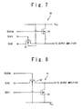
- FIG. 7 is a circuit diagram exemplifying a configuration of a bias signal control circuit.
- FIG. 8 is a circuit diagram exemplifying a configuration of a bias signal control circuit.
- FIG. 2 is a block diagram exemplifying a configuration of a liquid crystal display apparatus in this embodiment.
- the liquid crystal display apparatus 10 includes a liquid crystal display panel 1 , a data line driving circuit 2 , a scanning line driving circuit 3 , a power source circuit 4 and a control circuit 5 .
- the liquid crystal display panel 1 includes: data lines 6 that are laterally arrayed and longitudinally extended on the drawing; and scanning lines 7 that are longitudinally arrayed and laterally extended on the drawing. Also, The liquid crystal display panel 1 includes a plurality of pixels 8 arranged in a matrix shape. Each of the plurality of pixels 8 is arranged near each of intersections between the plurality of data lines 6 and the plurality of scanning lines 7 . Each of the plurality of pixels 8 includes a TFT (Thin Film Transistor) 11 , a pixel capacitor 12 and a liquid crystal element 13 . The gate of the TFT 11 is connected to the scanning line 7 . The source (drain) of the TFT 11 is connected to the data line 6 . Also, the drain (source) of the TFT 11 is connected to the pixel capacitor 12 and the liquid crystal element 13 . The pixel capacitor 12 and the liquid crystal element 13 are connected through a node 14 to a common electrode (not shown).
- TFT Thin Film Transistor
- the data line driving circuit 2 outputs signal voltages based on display data and drives the plurality of data lines 6 .
- the scanning line driving circuit 3 outputs selection/non-selection voltages of the TFTs 11 and drives the plurality of scanning lines 7 .
- the control circuit 5 controls timings of driving by the scanning line driving circuit 3 and the data line driving circuit 2 .
- the power source circuit 4 generates the signal voltages outputted by the data line driving circuit 2 and the selection/non-selection voltages outputted by the scanning line driving circuit 3 , and supplies them to the respective driving circuits.
- FIG. 3 is a block diagram showing a configuration of the data line driving circuit 2 in this embodiment.
- the display signal treated by the data line driving circuit 2 is a 6-bit digital display signal.
- the data line driving circuit 2 includes: a data register 15 ; a latching circuit 16 ; a D/A converter 18 ; a grayscale voltage generating circuit 17 ; and an output amplifier 19 .
- the data register 15 captures display signals R, G, B from outside.
- the latching circuit 16 latches a 6-bit digital signal in synchronization with a strobe signal ST.
- the D/A converter 18 is composed of digital/analog converters of parallel N stages.
- the grayscale voltage generating circuit 17 has a gamma conversion property matched with a property of the liquid crystal.
- the output amplifier 19 includes N number of output buffers 21 (voltage followers). Each of the N number of output buffers 21 supplies a voltage from the D/A converter 18 to the data line 6 .
- the plurality of output buffers 21 included in the output amplifier 19 is connected through bias wirings 23 to a bias circuit 22 .
- the bias circuit 22 outputs a bias voltage to the plurality of output buffers 21 .
- FIG. 4 is a block diagram exemplifying detailed configurations of the bias circuit 22 and related circuits in this embodiment.
- a plurality of switches (a first switch SW 1 to a sixth switch SW 6 ) is included in a route (the bias wiring 23 ) from the bias circuit 22 to the plurality of output buffers 21 .
- the bias wiring 23 includes bias wirings 23 - 0 to 23 - 8 .
- the bias wiring 23 - 0 connects the bias circuit 22 and both of the first and sixth switches SW 1 and SW 6 through nodes N 1 and N 2 , respectively.
- the bias wiring 23 - 1 connects the node N 1 to the output buffers 21 - 1 to 21 - 342 through bias signal control circuits 36 - 1 to 36 - 342 , respectively.
- the bias wiring 23 - 2 connects the first and second switches SW 1 and SW 2 to the output buffers 21 - 343 to 21 - 360 through bias signal control circuits 36 - 343 to 36 - 360 , respectively.
- the bias wiring 23 - 3 connects the second and third switches SW 2 and SW 3 to the output buffers 21 - 361 to 21 - 384 through bias signal control circuits 36 - 360 to 36 - 384 , respectively.
- the bias wiring 23 - 4 connects the third switch SW 3 and the bias circuits 22 to the output buffers 21 - 385 to 21 - 402 through bias signal control circuits 36 - 385 to 36 - 402 , respectively.
- the bias wiring 23 - 5 connects the bias circuit 22 and the fourth switch SW 4 to the output buffers 21 - 403 to 21 - 420 through bias signal control circuits 36 - 403 to 36 - 420 , respectively.
- the bias wiring 23 - 6 connects the fourth and fifth switches SW 4 and SW 5 to the output buffers 21 - 421 to 21 - 444 through bias signal control circuits 36 - 421 to 36 - 444 , respectively.
- the bias wiring 23 - 7 connects the fifth and sixth switches SW 5 and SW 6 to the output buffers 21 - 445 to 21 - 462 through bias signal control circuits 36 - 445 to 36 - 462 , respectively.
- the bias wiring 23 - 8 connects the node N 2 to the output buffers 21 - 463 to 21 - 804 through bias signal control circuits 36 - 463 to 36 - 804 , respectively.
- the bias signal control circuits 36 ( 36 - 1 to 36 - 804 ) are described later.
- each bias wiring may be arranged as one line in a chip layout.
- each of the plurality of switches is provided with a transfer gate and the like.
- the data line driving circuit 2 has a function for variably setting 4 kinds of output numbers.
- the output number of the data line driving circuit 2 in this embodiment is not limited.
- the bias circuit 22 is provided near the center of the chip of the data line driving circuit 2 and has a function for stopping an operation of the output buffer 21 near the center of the output column.
- the bias signal control circuits 36 - 1 to 36 - 342 maybe replaced with less than 342 or one bias signal control circuit 36 .
- the bias signal control circuits 36 - 343 to 36 - 360 may be replaced with less than 18 or one bias signal control circuit 36 .
- the bias signal control circuits 36 - 361 to 36 - 384 may be replaced with less than 24 or one bias signal control circuit 36 .
- the bias signal control circuits 36 - 385 to 36 - 402 may be replaced with less than 18 or one bias signal control circuit 36 .
- the bias signal control circuits 36 - 403 to 36 - 420 may be replaced with less than 18 or one bias signal control circuit 36 .
- the bias signal control circuits 36 - 421 to 36 - 444 may be replaced with less than 24 or one bias signal control circuit 36 .
- the bias signal control circuits 36 - 445 to 36 - 462 may be replaced with less than 18 or one bias signal control circuit 36 .
- the bias signal control circuits 36 - 463 to 36 - 804 may be replaced with less than 342 or one bias signal control circuit 36 .
- FIG. 5 is a table exemplifying a relation between states of the first switch SW 1 to the sixth switch SW 6 and the output numbers. As shown in the table in FIG. 5 , by switching the ON/OFF states of the plurality of switches (the first switch SW 1 to the sixth switch SW 6 ), it is possible to attain the various kinds of the output numbers ( 684 to 804 ).
- the bias wiring 23 - 0 in this embodiment is arranged from the bias circuit 22 to both of the first and sixth switches SW 1 and SW 6 , respectively.
- the first and sixth switches SW 1 and SW 6 are provided at boundaries between the left and right side portions and the other portions. In the left and right side portions, the number of output number switching actions is the smallest rather than the other portions.
- the bias wirings 23 - 0 and 23 - 1 directly connect the bias circuit 22 to the output buffers 21 - 1 to 21 - 342 .
- the bias wirings 23 - 0 and 23 - 8 directly connect the bias circuit 22 to the output buffers 21 - 463 to 21 - 804 .
- the expression of “directly connect” means “not connect through the switch”.
- the data line driving circuit 2 in this embodiment is configured such that the outputs from the output buffers 21 ahead of the boundaries (towards outside the IC) are fixed.
- the bias wiring 23 - 0 is connected to the respective output buffers 21 - 1 to 21 - 342 and 21 - 463 to 21 - 804 ahead of the boundaries.
- the switches (the first switch SW 1 to the sixth switch SW 6 ) for controlling connections of the bias wirings 23 - 1 to 23 - 8 for execution of the various switching actions.
- the first switch SW 1 switches on and off based on a first non-inversion signal TEST 1 and a first inversion signal TEST 1 B.
- the second switch SW 2 switches on and off based on a second non-inversion signal TEST 2 and a second inversion signal TEST 2 B.
- the third switch SW 3 switches on and off based on a third non-inversion signal TEST 3 and a third inversion signal TEST 3 B.
- the fourth switch SW 4 switches on and off based on a fourth non-inversion signal TEST 4 and a fourth inversion signal TEST 4 B.
- the fifth switch SW 5 switches on and off based on a fifth non-inversion signal TEST 5 and a fifth inversion signal TEST 5 B.
- the sixth switch SW 6 switches on and off based on a sixth non-inversion signal TEST 6 and a sixth inversion signal TEST 6 B.
- the bias wiring 23 connected to the output buffers 21 is wired up to the end of the maximal output (the output buffer 21 - 1 to 21 - 342 and 21 - 463 to 21 - 804 ). Then, the bias wiring 23 of the output inside the maximal output is wired through the switches (switches SW 1 to SW 6 ), and the output number is changed based on the control signal (non-inversion signals TEST 1 to TEST 6 and inversion signals TEST 1 B to TEST 6 B) supplied by the control circuit 5 . Also, when the output number is changed, the bias circuit 22 fixes a voltage of the bias wiring 23 connected to the bias signal control circuits 36 whose operation is stopped and consequently stops supplying the electric current to the corresponding output buffer 21 .
- the signal for controlling the plurality of switches (the first switch SW 1 to the sixth switch SW 6 ) is preferred to be used, when the electric current to the output buffer 21 is stopped (cut).
- the bias wirings 23 may be preferably arranged in symmetry with respect to a line passing through the bias circuit 22 and parallel to the plurality of data lines 6 .
- the plurality of switches may be preferably arranged in symmetry with respect to the line. More preferably, the line may pass through the middle of the bias circuit 23 .
- FIG. 6 is a circuit diagram exemplifying a configuration of the output buffer 21 in this embodiment.
- the output buffer 21 includes an amplifying stage 31 and an output stage 32 .
- this embodiment is exemplified with regard to a case in which transistors for receiving the input signals (Vin + , Vin ⁇ ) of the amplifying stage 31 are P-channel transistors.
- the configuration of the output buffer 21 in this embodiment is not limited to the circuit configuration shown in FIG. 6 .
- the output buffer 21 shown in FIG. 6 exemplifies a circuit whose operation is stopped based on the state of the first switch SW 1 .
- the amplifying stage 31 in the output buffer 21 includes an electric current source 33 .
- the electric current source 33 supplies a predetermined electric current to an input stage and a current mirror circuit, in response to a bias signal BIAS applied to the gate electrode from the bias circuit 22 through the bias signal control circuits 36 .
- a power source line voltage VDD as the bias signal BIAS is supplied to the output buffer 21 whose operation is stopped.
- the output stage 32 includes a first output control circuit 34 and a second output control circuit 35 .
- the first inversion signal TEST 1 B is supplied to the gate electrode of the first output control circuit 34
- the first non-inversion signal TEST 1 is supplied to the gate electrode of the second output control circuit 35 .
- the first non-inversion signal TEST 1 and the first inversion signal TEST 1 B are the signals for controlling the first switch SW 1 supplied by the control circuit 5 . Since the first non-inversion signal TEST 1 is set at a High level and the first inversion signal TEST 1 B is set at a Low level, the “Vout” of the output buffer 21 becomes Hi-Z (High Impedance).
- the bias signal BIAS itself outputted by the bias circuit 22 is supplied to the output buffer 21 whose operation is not stopped.
- the electric current source 33 supplies the steady-state electric current of the output buffer 21 .
- the first non-inversion signal TEST 1 is set at a Low level and the first inversion signal TEST 1 B is set at a High level, and the “Vout” based on the input signals (Vin + , Vin ⁇ ) is outputted to the data line 6 .
- FIG. 7 is a circuit diagram exemplifying a configuration of the bias signal control circuit 36 in this embodiment.
- the bias signal control circuit 36 is placed at the former stage of the output buffer 21 . That is, the bias signal control circuit 36 is placed between the bias circuit 22 and the output buffer 21 through the bias wiring 23 .
- the bias signal BIAS is supplied from the bias circuit 22 .
- the bias signal control circuit 36 sets the bias signal BIAS to the power source voltage or the ground (earth voltage) by, for example, connecting the bias wiring 23 to the power source voltage of the driver or the ground (earth voltage).
- the bias signal control circuit 36 by setting the bias wiring 23 to the power source voltage of the driver or the ground (earth voltage), stops (or forbids) the operation of the electric current source 33 in the output buffer 21 connected to the bias wiring 23 at the gate.
- the control circuit 5 sets the first non-inversion signal TEST 1 to the High level and sets the first inversion signal TEST 1 B to the Low level, a first transistor 37 is deactivated and a second transistor 38 is activated in the bias signal control circuit 36 . Therefore, in the bias signal control circuit 36 , the bias wiring 23 , to which the “BIAS” is supplied, is connected to the power source voltage VDD. It is also considered that the bias signal itself supplied by the bias circuit 22 is stopped and replaced with the power source voltage VDD.
- the control circuit 5 sets the first non-inversion signal TEST 1 to the Low level and sets the first inversion signal TEST 1 B to the High level.
- FIG. 8 is a circuit diagram exemplifying another configuration of the bias signal control circuit in this embodiment.
- the bias signal control circuit 41 in FIG. 8 is suitable for a case in which the transistors for receiving the input signals (Vin + , Vin ⁇ ) are N-channel transistors in the amplifying stage 31 in the output buffer 21 shown in FIG. 6 .
- the control circuit 5 sets the first non-inversion signal TEST 1 to the High level and sets the first inversion signal TEST 1 B to the Low level
- a third transistor 42 is deactivated and a fourth transistor 43 is activated in the bias signal control circuit 41 . Therefore, in the bias signal control circuit 41 , the bias wiring 23 , to which the “BIAS” is supplied, is connected to the VSS, and the electric current does not flow through the output buffer 21 .
- the data line driving circuit 2 in this embodiment sets the transistor in the output stage of the output buffer 21 (AMP) whose operation is stopped to the Hi-Z state and also cuts the electric current based on the bias signal for controlling the constant electric current source of the output buffer 21 (AMP).
- the data line driving circuit 2 cuts the electric current to the output buffer 21 whose operation is stopped, among the output buffers 21 in the output amplifier 19 .
- the switch can be used to switch the bias wirings, without using any complex circuit configuration. Then, since the electric current in the outputs that becomes unnecessary at that time can be cut, the reduction in the electric current consumption can be attained.
- This configuration enables the suppress in the electric current consumption of the output buffer 21 whose operation is stopped, by using the output switching, without any increase in the area on the layout of the bias wiring 23 .
- the driver circuit including the configuration in which the output numbers can be properly switched.
- the driver circuit including the configuration which can properly stop supplying the electric current to the outputs whose operation are stopped because the output numbers are switched.
Landscapes
- Engineering & Computer Science (AREA)
- Physics & Mathematics (AREA)
- Computer Hardware Design (AREA)
- General Physics & Mathematics (AREA)
- Theoretical Computer Science (AREA)
- Chemical & Material Sciences (AREA)
- Crystallography & Structural Chemistry (AREA)
- Control Of Indicators Other Than Cathode Ray Tubes (AREA)
- Liquid Crystal (AREA)
- Liquid Crystal Display Device Control (AREA)
Abstract
Description
Claims (17)
Applications Claiming Priority (2)
| Application Number | Priority Date | Filing Date | Title |
|---|---|---|---|
| JP2007-335042 | 2007-12-26 | ||
| JP2007335042A JP5354899B2 (en) | 2007-12-26 | 2007-12-26 | Display panel data line drive circuit, driver circuit, display device |
Publications (2)
| Publication Number | Publication Date |
|---|---|
| US20090167745A1 US20090167745A1 (en) | 2009-07-02 |
| US8330752B2 true US8330752B2 (en) | 2012-12-11 |
Family
ID=40797656
Family Applications (1)
| Application Number | Title | Priority Date | Filing Date |
|---|---|---|---|
| US12/314,490 Active 2031-06-08 US8330752B2 (en) | 2007-12-26 | 2008-12-11 | Data line driving circuit, driver IC and display apparatus |
Country Status (3)
| Country | Link |
|---|---|
| US (1) | US8330752B2 (en) |
| JP (1) | JP5354899B2 (en) |
| CN (1) | CN101471021A (en) |
Families Citing this family (2)
| Publication number | Priority date | Publication date | Assignee | Title |
|---|---|---|---|---|
| JP6272712B2 (en) * | 2014-03-05 | 2018-01-31 | ラピスセミコンダクタ株式会社 | Drive device for display device |
| US10902816B2 (en) * | 2017-04-10 | 2021-01-26 | Novatek Microelectronics Corp. | Integrated circuit for driving display panel and fan-out compensation method thereof |
Citations (9)
| Publication number | Priority date | Publication date | Assignee | Title |
|---|---|---|---|---|
| JPH07318897A (en) | 1994-05-20 | 1995-12-08 | Canon Inc | Active matrix liquid crystal display device and manufacturing method thereof |
| US6411162B2 (en) * | 2000-03-23 | 2002-06-25 | Kabushiki Kaisha Toshiba | Amplifier device and LCD device |
| US6496175B1 (en) * | 1999-04-05 | 2002-12-17 | Nec Corporation | Output circuit |
| US6759906B2 (en) * | 2001-07-23 | 2004-07-06 | Renesas Technology Corp. | High frequency power amplifier circuit device |
| US6850232B2 (en) * | 2001-08-28 | 2005-02-01 | Nec Electronics Corporation | Semiconductor device capable of internally generating bias changing signal |
| JP2005215007A (en) | 2004-01-27 | 2005-08-11 | Optrex Corp | Display apparatus |
| CN1892799A (en) | 2005-07-01 | 2007-01-10 | 三星电子株式会社 | Source driver for controlling a slew rate and a method for controlling the slew rate |
| US7173458B2 (en) * | 2003-09-03 | 2007-02-06 | Seiko Epson Corporation | Semiconductor device |
| US20080259017A1 (en) * | 2007-04-18 | 2008-10-23 | Cypress Semiconductor Corp. | Reducing power consumption in a liquid crystal display |
Family Cites Families (7)
| Publication number | Priority date | Publication date | Assignee | Title |
|---|---|---|---|---|
| JP3406884B2 (en) * | 1999-02-25 | 2003-05-19 | 株式会社東芝 | Integrated circuit device and liquid crystal display device using the same |
| JP4770001B2 (en) * | 2000-06-22 | 2011-09-07 | 日本テキサス・インスツルメンツ株式会社 | Driving circuit and voltage driver |
| JP3744819B2 (en) * | 2001-05-24 | 2006-02-15 | セイコーエプソン株式会社 | Signal driving circuit, display device, electro-optical device, and signal driving method |
| JP2003229726A (en) * | 2002-02-06 | 2003-08-15 | Nec Kansai Ltd | Semiconductor integrated circuit device for driving liquid crystal |
| KR100602359B1 (en) * | 2004-09-01 | 2006-07-14 | 매그나칩 반도체 유한회사 | Source driver with multi-channel shift register |
| JP2007140005A (en) * | 2005-11-17 | 2007-06-07 | Matsushita Electric Ind Co Ltd | Bias voltage generation circuit |
| JP5238230B2 (en) * | 2007-11-27 | 2013-07-17 | ルネサスエレクトロニクス株式会社 | Driver and display device |
-
2007
- 2007-12-26 JP JP2007335042A patent/JP5354899B2/en active Active
-
2008
- 2008-12-11 US US12/314,490 patent/US8330752B2/en active Active
- 2008-12-17 CN CNA2008101856343A patent/CN101471021A/en active Pending
Patent Citations (11)
| Publication number | Priority date | Publication date | Assignee | Title |
|---|---|---|---|---|
| JPH07318897A (en) | 1994-05-20 | 1995-12-08 | Canon Inc | Active matrix liquid crystal display device and manufacturing method thereof |
| US6496175B1 (en) * | 1999-04-05 | 2002-12-17 | Nec Corporation | Output circuit |
| US6411162B2 (en) * | 2000-03-23 | 2002-06-25 | Kabushiki Kaisha Toshiba | Amplifier device and LCD device |
| US6759906B2 (en) * | 2001-07-23 | 2004-07-06 | Renesas Technology Corp. | High frequency power amplifier circuit device |
| US6850232B2 (en) * | 2001-08-28 | 2005-02-01 | Nec Electronics Corporation | Semiconductor device capable of internally generating bias changing signal |
| US7173458B2 (en) * | 2003-09-03 | 2007-02-06 | Seiko Epson Corporation | Semiconductor device |
| JP2005215007A (en) | 2004-01-27 | 2005-08-11 | Optrex Corp | Display apparatus |
| CN1892799A (en) | 2005-07-01 | 2007-01-10 | 三星电子株式会社 | Source driver for controlling a slew rate and a method for controlling the slew rate |
| US20070008009A1 (en) * | 2005-07-01 | 2007-01-11 | Samsung Electronics Co., Ltd. | Source driver for controlling a slew rate and a method for controlling the slew rate |
| US7808468B2 (en) | 2005-07-01 | 2010-10-05 | Samsung Electronics Co., Ltd. | Source driver for controlling a slew rate and a method for controlling the slew rate |
| US20080259017A1 (en) * | 2007-04-18 | 2008-10-23 | Cypress Semiconductor Corp. | Reducing power consumption in a liquid crystal display |
Non-Patent Citations (2)
| Title |
|---|
| Chinese Office Action dated Dec. 1, 2011, with English translation. |
| Japanese Notification for Reasons for Refusal dated May 17, 2012, with partial English-language translation. |
Also Published As
| Publication number | Publication date |
|---|---|
| CN101471021A (en) | 2009-07-01 |
| JP5354899B2 (en) | 2013-11-27 |
| JP2009157094A (en) | 2009-07-16 |
| US20090167745A1 (en) | 2009-07-02 |
Similar Documents
| Publication | Publication Date | Title |
|---|---|---|
| KR100608106B1 (en) | LCD and source line repair method having a source line repair function | |
| US6753731B2 (en) | Operation amplifier circuit, drive circuit and method of controlling operation amplifier circuit | |
| US8368672B2 (en) | Source driver, electro-optical device, and electronic instrument | |
| US8576257B2 (en) | Integrated circuit device, electro-optical device, and electronic instrument | |
| US6982706B1 (en) | Liquid crystal driving circuit, semiconductor integrated circuit device, reference voltage buffering circuit, and method for controlling the same | |
| JP5137321B2 (en) | Display device, LCD driver, and driving method | |
| US20110242145A1 (en) | Display device, differential amplifier, and data line drive method for display device | |
| US20120019502A1 (en) | Source driver for a liquid crystal display device and liquid crystal display device using the same | |
| US9202425B2 (en) | Device circuit and display apparatus having operational amplifiers with parasitic diodes | |
| US20090128476A1 (en) | Gate driving circuit and display device including the same | |
| US8558852B2 (en) | Source driver, electro-optical device, and electronic instrument | |
| CN102446482A (en) | Output circuit, data driver circuit and display device | |
| US20120092322A1 (en) | Liquid crystal display drive circuit and method for driving same | |
| US7808320B1 (en) | Buffer amplifier | |
| US20090096816A1 (en) | Data driver, integrated circuit device, and electronic instrument | |
| US20090160849A1 (en) | Integrated circuit device, electro-optical device, and electronic instrument | |
| US7986290B2 (en) | Output stage and related logic control method applied to source driver/chip | |
| KR100862945B1 (en) | Chip On Glass Liquid Crystal Display | |
| US11862058B2 (en) | Load driving circuit, display driver, display apparatus and semiconductor device | |
| US8330752B2 (en) | Data line driving circuit, driver IC and display apparatus | |
| US20110227905A1 (en) | Driver and display device using the same | |
| JP6205112B2 (en) | Source driver, liquid crystal display device using the same, and electronic device | |
| US20060125743A1 (en) | LCD panel driving device and conductive pattern on LCD panel therefore | |
| JP3573055B2 (en) | Display drive device, display device, and portable electronic device | |
| JP2009198970A (en) | Driving device of liquid crystal display panel |
Legal Events
| Date | Code | Title | Description |
|---|---|---|---|
| AS | Assignment |
Owner name: NEC ELECTRONICS CORPORATION, JAPAN Free format text: ASSIGNMENT OF ASSIGNORS INTEREST;ASSIGNOR:ENJOU, HIROYASU;REEL/FRAME:022029/0200 Effective date: 20081203 |
|
| AS | Assignment |
Owner name: RENESAS ELECTRONICS CORPORATION, JAPAN Free format text: CHANGE OF NAME;ASSIGNOR:NEC ELECTRONICS CORPORATION;REEL/FRAME:025214/0678 Effective date: 20100401 |
|
| STCF | Information on status: patent grant |
Free format text: PATENTED CASE |
|
| FPAY | Fee payment |
Year of fee payment: 4 |
|
| AS | Assignment |
Owner name: RENESAS ELECTRONICS CORPORATION, JAPAN Free format text: CHANGE OF ADDRESS;ASSIGNOR:RENESAS ELECTRONICS CORPORATION;REEL/FRAME:044928/0001 Effective date: 20150806 |
|
| MAFP | Maintenance fee payment |
Free format text: PAYMENT OF MAINTENANCE FEE, 8TH YEAR, LARGE ENTITY (ORIGINAL EVENT CODE: M1552); ENTITY STATUS OF PATENT OWNER: LARGE ENTITY Year of fee payment: 8 |
|
| MAFP | Maintenance fee payment |
Free format text: PAYMENT OF MAINTENANCE FEE, 12TH YEAR, LARGE ENTITY (ORIGINAL EVENT CODE: M1553); ENTITY STATUS OF PATENT OWNER: LARGE ENTITY Year of fee payment: 12 |