US8325502B2 - Self-supply circuit and method for a voltage converter - Google Patents

Self-supply circuit and method for a voltage converter Download PDF

Info

Publication number
US8325502B2
US8325502B2 US12/324,548 US32454808A US8325502B2 US 8325502 B2 US8325502 B2 US 8325502B2 US 32454808 A US32454808 A US 32454808A US 8325502 B2 US8325502 B2 US 8325502B2
Authority
US
United States
Prior art keywords
precharge
charge
controller
signal
voltage
Prior art date
Legal status (The legal status is an assumption and is not a legal conclusion. Google has not performed a legal analysis and makes no representation as to the accuracy of the status listed.)
Active, expires
Application number
US12/324,548
Other versions
US20090140712A1 (en
Inventor
Salvatore Giombanco
Salvatore Tumminaro
Current Assignee (The listed assignees may be inaccurate. Google has not performed a legal analysis and makes no representation or warranty as to the accuracy of the list.)
STMicroelectronics SRL
Original Assignee
STMicroelectronics SRL
Priority date (The priority date is an assumption and is not a legal conclusion. Google has not performed a legal analysis and makes no representation as to the accuracy of the date listed.)
Filing date
Publication date
Application filed by STMicroelectronics SRL filed Critical STMicroelectronics SRL
Assigned to STMICROELECTRONICS S.R.L. reassignment STMICROELECTRONICS S.R.L. ASSIGNMENT OF ASSIGNORS INTEREST (SEE DOCUMENT FOR DETAILS). Assignors: GIOMBANCO, SALVATORE, TUMMINARO, SALVATORE
Publication of US20090140712A1 publication Critical patent/US20090140712A1/en
Application granted granted Critical
Publication of US8325502B2 publication Critical patent/US8325502B2/en
Active legal-status Critical Current
Adjusted expiration legal-status Critical

Links

Images

Classifications

    • HELECTRICITY
    • H02GENERATION; CONVERSION OR DISTRIBUTION OF ELECTRIC POWER
    • H02MAPPARATUS FOR CONVERSION BETWEEN AC AND AC, BETWEEN AC AND DC, OR BETWEEN DC AND DC, AND FOR USE WITH MAINS OR SIMILAR POWER SUPPLY SYSTEMS; CONVERSION OF DC OR AC INPUT POWER INTO SURGE OUTPUT POWER; CONTROL OR REGULATION THEREOF
    • H02M3/00Conversion of DC power input into DC power output
    • H02M3/22Conversion of DC power input into DC power output with intermediate conversion into AC
    • H02M3/24Conversion of DC power input into DC power output with intermediate conversion into AC by static converters
    • H02M3/28Conversion of DC power input into DC power output with intermediate conversion into AC by static converters using discharge tubes with control electrode or semiconductor devices with control electrode to produce the intermediate AC
    • H02M3/325Conversion of DC power input into DC power output with intermediate conversion into AC by static converters using discharge tubes with control electrode or semiconductor devices with control electrode to produce the intermediate AC using devices of a triode or a transistor type requiring continuous application of a control signal
    • H02M3/335Conversion of DC power input into DC power output with intermediate conversion into AC by static converters using discharge tubes with control electrode or semiconductor devices with control electrode to produce the intermediate AC using devices of a triode or a transistor type requiring continuous application of a control signal using semiconductor devices only
    • H02M3/33507Conversion of DC power input into DC power output with intermediate conversion into AC by static converters using discharge tubes with control electrode or semiconductor devices with control electrode to produce the intermediate AC using devices of a triode or a transistor type requiring continuous application of a control signal using semiconductor devices only with automatic control of the output voltage or current, e.g. flyback converters
    • HELECTRICITY
    • H02GENERATION; CONVERSION OR DISTRIBUTION OF ELECTRIC POWER
    • H02MAPPARATUS FOR CONVERSION BETWEEN AC AND AC, BETWEEN AC AND DC, OR BETWEEN DC AND DC, AND FOR USE WITH MAINS OR SIMILAR POWER SUPPLY SYSTEMS; CONVERSION OF DC OR AC INPUT POWER INTO SURGE OUTPUT POWER; CONTROL OR REGULATION THEREOF
    • H02M1/00Details of apparatus for conversion
    • H02M1/36Means for starting or stopping converters
    • HELECTRICITY
    • H02GENERATION; CONVERSION OR DISTRIBUTION OF ELECTRIC POWER
    • H02MAPPARATUS FOR CONVERSION BETWEEN AC AND AC, BETWEEN AC AND DC, OR BETWEEN DC AND DC, AND FOR USE WITH MAINS OR SIMILAR POWER SUPPLY SYSTEMS; CONVERSION OF DC OR AC INPUT POWER INTO SURGE OUTPUT POWER; CONTROL OR REGULATION THEREOF
    • H02M1/00Details of apparatus for conversion
    • H02M1/0003Details of control, feedback or regulation circuits
    • H02M1/0006Arrangements for supplying an adequate voltage to the control circuit of converters

Definitions

  • An embodiment of the present disclosure relates to a self-supply circuit and method for a voltage converter, and more precisely for a switched-mode voltage converter, controlled in pulse-width modulation (PWM).
  • PWM pulse-width modulation
  • switched-mode voltage converters which are preferred for their high efficiency and their reduced size as compared to classic linear converters, usually implement a self-supply technique that enables, starting from non-regulated input voltages, regulated output voltages to be obtained having an amplitude greater or smaller than the input voltage.
  • flyback One of the most common types of switched-mode voltage converters is the isolated accumulation (“flyback”) type.
  • a flyback voltage converter enables conversion of a first voltage value (present on an input of the converter) into a second voltage value (supplied on the output of the converter), maintaining the input and output of the converter galvanically isolated by the use of a transformer.
  • FIG. 1 shows a circuit diagram of a known voltage converter 1 , of a flyback type.
  • the voltage converter 1 has an input 2 to which an input voltage V in (for example, supplied by a rectifier circuit, not illustrated, starting from the mains voltage) is applied, and an output 3 supplying an output voltage V out , and comprises a transformer 4 , having a primary side and a secondary side, which is electrically isolated from the primary side.
  • the transformer 4 has a primary winding 4 a coupled to the input 2 , a secondary winding 4 b coupled to the output 3 by interposition of a first diode 6 , and an auxiliary winding 4 c (the latter set on the primary side of the transformer 4 ).
  • An output capacitor 7 is coupled to the output 3 .
  • a main transistor 10 in particular an N-channel MOS transistor, is coupled between an internal node 8 , which is in turn coupled to the primary winding 4 a , and a reference terminal 9 (for example, a ground terminal).
  • a bulk capacitor 11 is coupled between the input 2 and the reference terminal 9 .
  • the voltage converter 1 further comprises: a PWM controller 12 , used for regulation of the output voltage V out , having a supply terminal 13 , which receives a supply voltage V cc and is coupled to the auxiliary winding 4 c via the interposition of a second diode 14 , and an output terminal, which is coupled to the gate terminal of the main transistor 10 and supplies a PWM signal for controlling opening and closing of the main transistor 10 ; and a self-supply circuit 15 , having an input terminal coupled to the input 2 of the voltage converter 1 , and an output terminal, which coincides with the supply terminal 13 of the PWM controller 12 and supplies the supply voltage V cc .
  • a PWM controller 12 used for regulation of the output voltage V out , having a supply terminal 13 , which receives a supply voltage V cc and is coupled to the auxiliary winding 4 c via the interposition of a second diode 14 , and an output terminal, which is coupled to the gate terminal of the main transistor 10 and supplies a PWM signal for controlling
  • the self-supply circuit 15 comprises: an accumulation capacitor 16 , coupled between the supply terminal 13 and the reference terminal 9 ; and a start-up resistor 18 coupled between the input terminal 2 of the voltage converter and the supply terminal 13 .
  • the function of the self-supply circuit 15 is that of supplying the PWM controller 12 to enable it to regulate the output voltage V out .
  • the accumulation capacitor 16 is initially charged by the input voltage V in , through the start-up resistor 18 .
  • the PWM controller 12 switches on when the value of the voltage on the accumulation capacitor 16 reaches a first threshold value V ccon , for example, equal to 13.5 V.
  • the PWM controller 12 receives the supply voltage V cc directly from the auxiliary winding 4 c of the transformer 4 .
  • the start-up resistor 18 is used in the initial turn-on phase (start-up) of the voltage converter 1 for supplying the turn-on supply to the PWM controller 12 .
  • a current flows through the start-up resistor 18 also at the end of the initial start-up phase, causing a considerable dissipation of power and reducing the efficiency of the voltage converter 1 .
  • the auxiliary winding 4 c is also used (in a known way that is not described in detail herein) for supplying a feedback signal to the PWM controller 12 , for regulating both the output voltage V out and the output current I out .
  • the voltage on the auxiliary winding 4 c might not have a value sufficient for supplying the PWM controller 12 . Consequently, also during the switching phase in which the PWM controller 12 is active, the PWM controller 12 is self-supplied through the start-up resistor 18 , thus increasing the total power dissipation.
  • FIG. 2 shows a different circuit embodiment of the self-supply circuit 15 of the voltage converter 1 (the remaining elements of the voltage converter, which are present also in this embodiment, are not illustrated again here for clarity reasons).
  • the self-supply circuit 15 comprises: the accumulation capacitor 16 (previously described); an auxiliary transistor 21 , in particular an N-channel MOS transistor having a drain terminal coupled to the input 2 of the voltage converter 1 and receiving the input voltage V in ; a first biasing resistor 22 , having, for example, a value of resistance of 15 M ⁇ and coupled between the input 2 of the voltage converter 1 and the gate terminal of the auxiliary transistor 21 ; a second biasing resistor 23 , coupled between the gate terminal of the auxiliary transistor 21 and the reference terminal 9 ; a current generator 24 , which is coupled between the source terminal of the auxiliary transistor 21 and the supply terminal 13 of the PWM controller 12 , via the interposition of a third diode 25 , and has a control terminal; and a switch 26 , coupled between the gate terminal of the auxiliary transistor 21 and the reference terminal 9 .
  • the self-supply circuit 15 further comprises a control logic 28 , having a first input coupled to the gate terminal of the auxiliary transistor 21 , a second input coupled to the supply terminal 13 , a first output supplying a control signal V cc — OK to a control terminal of the switch 26 , and a second output supplying to the control terminal of the current generator 24 an activation signal HV_EN.
  • a control logic 28 having a first input coupled to the gate terminal of the auxiliary transistor 21 , a second input coupled to the supply terminal 13 , a first output supplying a control signal V cc — OK to a control terminal of the switch 26 , and a second output supplying to the control terminal of the current generator 24 an activation signal HV_EN.
  • the control logic 28 turns on the current generator 24 via the activation signal HV_EN, enabling a current I charge to flow through the auxiliary transistor 21 .
  • This current I charge for example, having a value of 1 mA, charges the accumulation capacitor 16 , raising the supply voltage V cc across its terminals in a substantially linear way.
  • the signal V cc — OK generated by the control logic 28 closes the switch 26 , causing turning-off of the auxiliary transistor 21 and interruption of the flow of current I charge through the same auxiliary transistor 21 and the current generator 24 .
  • the PWM controller 12 ( FIG. 1 ) is then supplied by the energy stored in the accumulation capacitor 16 , as long as the auxiliary winding 4 c generates a voltage sufficiently high to sustain the operations of regulation of the controller.
  • the residual consumption of the self-supply circuit 15 is hence due only to the presence of the first biasing resistor 22 , and is typically from 50 to 70 times lower than that of the circuit of FIG. 1 .
  • the self-supply circuit 15 also intervenes for charging the accumulation capacitor 16 during the switching phase of the main transistor 10 ( FIG. 1 ), in the case where the voltage on the auxiliary winding is not sufficient to supply the supply voltage V cc , for example, in the case of operation as a battery-charger, when the battery is run down or in the presence of overload at the output.
  • the control logic 28 controls opening of the switch 26 by means of the signal V cc — OK , and enables the current generator 24 by means of the signal HV_EN so as to charge the accumulation capacitor 16 via the current I charge .
  • the auxiliary transistor 21 and the main transistor 10 share the drain terminal.
  • the drain terminal is coupled to the internal node 8 ( FIG. 1 ), which is in turn coupled to the primary winding 4 a of the transformer 4 , and is at a voltage which is not constant (i.e., which switches between a value of approximately 0 V and the value of the input voltage V in ).
  • the self-supply circuit 15 of FIG. 3 thus enables charging of the accumulation capacitor 16 only when the main transistor 10 is turned off, i.e., when the voltage of the aforesaid drain terminal (or, in a similar way of the internal node 8 ) is high and equal to the value of the input voltage V in . Consequently, in the case where the self-supply circuit 15 is also used for self-supply of the PWM controller 12 through the accumulation capacitor 16 during the switching phase of the PWM controller 12 , the current I charge can charge the accumulation capacitor 16 only during the OFF phase of the switching period, when the voltage of the drain terminal is high.
  • This condition can jeopardize proper operation of the self-supply circuit 15 , especially for high values of duty cycle (higher than 50%) of the switching signal that regulates operation of the voltage converter 1 , and consequently considerably limits the maximum value of duty cycle that can be obtained.
  • the auxiliary transistor 21 should be able to turn on rapidly during turning-off of the main transistor 10 in order to maximize the useful time (substantially corresponding to the OFF phase of the switching signal) for charging the accumulation capacitor 16 .
  • the switching rate of the auxiliary transistor 21 is limited by the gate capacitance of the latter and by the presence of the first biasing resistor 22 , the value of which is commonly chosen high (for example, equal to 15 M ⁇ ) in order to minimize the losses.
  • the voltage on the internal node 8 is approximately 0 V and the auxiliary transistor 21 is off.
  • the signal V cc — OK generated by the control logic 28 controls opening of the switch 26 , the voltage on the drain terminal of the auxiliary transistor 21 starts to increase, and the gate capacitor of the same auxiliary transistor 21 is charged, first by the injection of charge coming from the capacitance between the drain and gate terminals and then, when the voltage on the drain terminal reaches a sufficiently high value, through the biasing resistor 22 . Both of these contributions of charge may not be, however, sufficient to turn on the auxiliary transistor 21 completely, and to supply the current I charge required by the current generator 24 , in a reasonable time.
  • Embodiments of the present disclosure include a self-supply circuit and method that will be free from the drawbacks described above, and in particular that will enable self-supply to be guaranteed in a voltage converter without setting any limitations on the duty cycle.
  • FIG. 1 shows a circuit diagram of a flyback voltage converter of a known type
  • FIG. 2 shows a circuit diagram of a self-supply circuit of the voltage converter of FIG. 1 ;
  • FIG. 3 shows a different circuit diagram, of a known type, of the self-supply circuit
  • FIG. 4 shows part of a circuit diagram of a voltage converter with highlighted therein a self-supply circuit, made according to an embodiment of the present disclosure
  • FIG. 5 shows a possible circuit embodiment of a precharge stage within the self-supply circuit of FIG. 4 ;
  • FIGS. 6 and 7 show the plots in time of the waveforms of electrical signals involved during a precharge step in the voltage converter of FIG. 4 ;
  • FIG. 8 shows a possible embodiment of a precharge control block inside the precharge stage of FIG. 5 ;
  • FIG. 9 shows the plots of electrical signals involved during the precharge step
  • FIG. 10 shows a first embodiment of a portion of the precharge-control block
  • FIG. 11 shows the plots of the signals involved during the precharge step, using the precharge control block of FIG. 10 ;
  • FIG. 12 shows a second embodiment of the precharge control block
  • FIG. 13 shows the plots of the signals involved during the precharge step, using the precharge control block of FIG. 12 ;
  • FIG. 14 shows a third embodiment of the precharge control block
  • FIG. 15 shows the plots of the signals involved during the precharge step, using the precharge control block of FIG. 14 .
  • FIG. 4 shows a self-supply circuit 30 , made according to an embodiment of the present disclosure. Elements that have already been described with reference to the known art are designated by the same reference numbers and are not described again.
  • the self-supply circuit 30 may find use in a voltage converter 1 of the type described with reference to FIG. 1 (not illustrated in FIG. 4 ).
  • the self-supply circuit 30 differs from the one described in FIG. 3 , in so far as it comprises a precharge stage 31 coupled (in this embodiment coupled) directly to the gate terminal of the auxiliary transistor 21 .
  • a precharge stage 31 coupled (in this embodiment coupled) directly to the gate terminal of the auxiliary transistor 21 .
  • the second biasing resistor 23 and the control logic 28 are present (for greater clarity, these elements are not shown again in the subsequent figures).
  • the precharge stage 31 enables a rapid switching of the auxiliary transistor 21 to be obtained during each switching cycle, in so far as it has the function of precharging the capacitance between the gate and source terminals of the auxiliary transistor 21 , whilst the voltage on the drain terminal is still at a low value, during or at the end of the turning-on phase (ON phase of the switching period) of the main transistor 10 .
  • the auxiliary transistor 21 is already turned on, and the current generator 24 can generate the current I charge for charging the accumulation capacitor 16 without appreciable time delays.
  • the precharge stage 31 has also the function of controlling turning-off of the auxiliary transistor 21 in order to interrupt the flow of the current I charge .
  • the value of the current I charge generated by the current generator 24 is determined as a function of the maximum duty cycle D max of the switching signal, and of the current consumption I cons of the voltage converter 1 , and must satisfy the following condition:
  • the self-supply operation is carried out without limiting the duty cycle of the switching signal.
  • the precharge stage 31 comprises: a first precharge switch 33 , coupled between the gate terminal of the auxiliary transistor 21 and the reference terminal 9 ; a second precharge switch 34 , coupled between the source terminal of the auxiliary transistor 21 and the reference terminal 9 ; a third precharge switch 35 , coupled between the gate terminal of the auxiliary transistor 21 and the supply terminal 13 of the PWM controller 12 (and hence to the accumulation capacitor 16 ); and a precharge control block 36 , designed to generate respective control signals for the first, second, and third precharge switches 33 , 34 , 35 such as to implement self-supply management.
  • the first precharge switch 33 is controlled in opening and closing by a logic signal HV_EN_G
  • the second precharge switch 34 is controlled in opening and closing by a logic signal HV_EN_S
  • the third precharge switch 35 is controlled in opening and closing by a logic signal EN_PRE.
  • the first and second precharge switches 33 , 34 are closed (signals HV_EN_G and HV_EN_S high), and the third precharge switch 35 is open (signal EN_PRE low), thus connecting the source and gate terminals of the auxiliary transistor 21 to the reference terminal 9 .
  • the first precharge switch 33 is controlled in opening (signal HV_EN_G low), whilst the second and third precharge switches 34 , 35 are controlled in closing (signals HV_EN_S and EN_PRE high).
  • the source terminal of the auxiliary transistor 21 is coupled to the reference terminal 9 , and the gate terminal directly to the supply voltage V cc , thus starting precharging of the gate-source capacitance of the auxiliary transistor 21 to the supply voltage V cc .
  • the second and third precharge switches 34 , 35 are controlled in opening (signals HV_EN_S and EN_PRE low), given that the precharging phase can be considered completed. It should be noted that the auxiliary transistor 21 , in this situation, is already turned on, and the charge current I charge can immediately flow (as soon as the voltage at the internal node 8 becomes high) through the current generator 24 , thus charging the accumulation capacitor 16 so that the entire OFF phase of the switching signal is exploited.
  • FIG. 6 shows the waveforms of the voltage on the drain terminal, designated by V (drain) , on the gate terminal, designated by V (gate) , and on the source terminal, designated by V (source) , of the auxiliary transistor 21 , and of the charge current I charge .
  • FIG. 7 shows an enlarged portion of the aforesaid waveforms, approximately upon switching at the instant of time t 2 , together with the plot of the logic signals HV_EN_G, HV_EN_S, and EN_PRE, with highlighted the precharging phase. It should be noted that the voltage on the gate terminal V (gate) starts to rise after switching of the signal EN_PRE to the high value, as a result of the precharging operation.
  • FIG. 8 shows a possible embodiment of the precharge-control block 36 of the precharge stage 31 , which comprises a precharge logic 38 , and an end-of-precharge controller 39 .
  • the end-of-precharge controller 39 controls, as will be described in detail hereinafter, the appropriate instant of time at which the precharging phase of the auxiliary transistor 21 stops, generating an end-of-precharge signal END_PRE.
  • the precharge logic 38 receives at input, from the end-of-precharge controller 39 , the end-of-precharge signal END_PRE, and, from the PWM controller 12 , a control signal Q G , which is a function of a signal that controls, in a per-se known manner (for example, through a driver), the main transistor 10 .
  • the precharge logic 38 according to the end-of-precharge signal END_PRE and to the control signal Q G , generates the logic signals HV_EN_G, HV_EN_S, EN_PRE for management of the precharging phase.
  • FIG. 9 shows in detail the plots of the control signal Q G , of the logic signal EN_PRE, of the voltage on the gate terminal V (gate) and of the voltage on the drain terminal V (drain) of the main transistor 10 .
  • the control signal Q G when the control signal Q G is active high, the main transistor 10 is in conduction (the voltage signal on the gate terminal V (gate) is high), whilst the voltage signal on the drain terminal V (drain) and the logic signal EN_PRE have a low value, indicating that the precharging phase has not started yet.
  • the precharging phase is disabled by the end-of-precharge controller 39 at the instant of time t 2 , before or at the end of a delay interval T delay that represents a delay of turning-off of the main transistor 10 , after which the voltage signal on the gate terminal V (gate) drops below the threshold voltage V TH of the main transistor 10 , and the voltage on the drain terminal V (drain) starts to increase. It is in fact expedient for the precharging phase to terminate before the voltage signal on the drain terminal V (drain) starts to increase so as to prevent the phenomenon of cross-conduction between the drain terminal of the auxiliary transistor 21 and the reference terminal 9 .
  • the end-of-precharge controller here designated by 39 ′, includes a comparator device 42 , which receives on a first input a reference voltage V REF , and on a second input the voltage on the gate terminal V (gate) taken on the gate terminal of the main transistor 10 , and supplies at output the end-of-precharge signal END_PRE.
  • the end-of-precharge signal END_PRE assumes a logic value (for example, high) indicating the end of the precharging interval.
  • the value of the reference voltage V REF may be chosen so as to be higher than the threshold-voltage value V TH of the main transistor 10 , given that the voltage on the drain terminal V (drain) starts to increase when the voltage on the gate terminal V (gate) drops below the threshold-voltage value V TH .
  • the end-of-precharge controller 39 ′′ comprises in this case a pulse generator 44 , which receives on an input thereof the control signal Q G , and generates at output the end-of-precharge signal END_PRE, here of an impulsive type, for example, having a pulse duration T pulse equal to or shorter than the delay interval T delay .
  • the end-of-precharge controller 39 ′′ is configured to generate the end-of-precharge signal END_PRE when the control signal Q G assumes a low value.
  • the precharge is stopped (the logic signal EN_PRE is brought to the low value) at the falling edge of the end-of-precharge signal END_PRE.
  • FIG. 14 shows a third embodiment of the end-of-precharge controller, designated by 39 ′′′, in the case where the PWM controller 12 drives the main transistor 10 in such a way as to guarantee the so-called “soft-switching”.
  • the end-of-precharge controller 39 ′′′ comprises: a negative-derivative detector (NDD) 45 , of a known type and not described in detail, which receives on an input thereof the voltage on the gate terminal V (gate) and supplies on an output thereof a negative-derivative signal NEG_DER, as a function of the sign of the derivative of the voltage on the gate terminal; and a counter block 48 , which receives at input the negative-derivative signal NEG_DER and supplies on an output thereof the end-of-precharge signal END_PRE.
  • NDD negative-derivative detector
  • the control signal Q G switches from the high level to the low level, controlling turning-off of the main transistor 10 .
  • the logic signal EN_PRE assumes a high value, indicating start of the precharging interval.
  • the voltage on the gate terminal V (gate) starts to decrease and the negative-derivative signal NEG_DER assumes a high value, indicating that the derivative of the signal has assumed a negative value.
  • the voltage on the gate terminal V (gate) assumes a stationary value.
  • the negative-derivative signal NEG_DER returns to the low value, and the voltage on the drain terminal V (drain) starts to increase slowly.
  • the Miller effect terminates (instant of time t 4 )
  • the voltage on the gate terminal V (gate) starts to decrease again
  • the voltage on the drain terminal V (drain) increases rapidly, and a new rising edge of the negative-derivative signal NEG_DER determines the end of the precharging interval (the logic signal EN_PRE assumes a low value).
  • the counter block 48 detects the occurrence of the second pulse generated by the negative-derivative detector 45 , and consequently generates the end-of-precharge signal END_PRE.
  • precharging of the gate terminal of the auxiliary transistor 21 that manages the precharging phase enables maximization of the time interval useful for charging the accumulation capacitor 16 , so as to guarantee proper self-supply of the controller 12 of the voltage converter 1 without imposing limitations on the duty cycle of the switching signal.
  • the auxiliary transistor 21 is already turned on and the current generator 24 can supply the current I charge to the accumulation capacitor 16 without appreciable time delays (after the main transistor is turned off).
  • embodiments described above, as well as other embodiments may be used irrespective of: the modality of energy transfer between the source and load, at a fixed or variable frequency; the particular circuit solution used for implementing operation of the individual blocks of the control circuit; the type of control switch; and the feedback mode envisaged on the primary side of the transformer.
  • T delay and T pulse may extend to or beyond a time when V (gate) of the main transistor 10 equals V TH of the main transistor.
  • some or all of the components in the circuits of FIGS. 1-5 , 8 , 10 , 12 , and 14 may be discrete components, disposed on the same integrated circuit (IC) as others of the components, or disposed on ICs that are different from ICs on which others of the components are disposed.
  • IC integrated circuit

Landscapes

  • Engineering & Computer Science (AREA)
  • Power Engineering (AREA)
  • Dc-Dc Converters (AREA)
  • Direct Current Feeding And Distribution (AREA)

Abstract

An embodiment of a self-supply circuit, for a voltage converter that converts an input voltage into an output voltage and has a main switch and a controller, designed to control switching of the main switch for controlling the output voltage; the self-supply circuit is provided with: a charge accumulator, which is connected to the controller and supplies a self-supply voltage to the same controller; a generator, which supplies a charge current to the charge accumulator; and an auxiliary switch, which has a first conduction terminal in common with a respective conduction terminal of the main switch and is operable so as to control transfer of the charge current to the charge accumulator. In particular, the self-supply circuit is provided with a precharge stage, connected to the auxiliary switch, which carries out a precharging of an intrinsic capacitance of the auxiliary switch before a turning-off transient of the main switch ends.

Description

PRIORITY CLAIM
The present application claims the benefit of Italian Patent Application Serial No.: TO2007A000860, filed Nov. 29, 2007, which application is incorporated herein by reference in its entirety.
RELATED APPLICATION DATA
This application is related to the U.S. patent application Ser. No. 12/324,194 entitled ISOLATED VOLTAGE CONVERTER WITH FEEDBACK ON THE PRIMARY WINDING, AND CORRESPONDING METHOD FOR CONTROLLING THE OUTPUT VOLTAGE, filed Nov. 26, 2008, application Ser. No. 12/324,062 entitled ISOLATED VOLTAGE CONVERTER WITH FEEDBACK ON THE PRIMARY WINDING, AND CORRESPONDING METHOD FOR CONTROLLING THE OUTPUT VOLTAGE, filed Nov. 26, 2008 and application Ser. No. 12/324,412 entitled ISOLATED VOLTAGE CONVERTER WITH FEEDBACK ON THE PRIMARY WINDING AND PASSIVE SNUBBER NETWORK, AND CORRESPONDING CONTROL METHOD, filed Nov. 26, 2008 and which are incorporated herein by reference in their entireties.
TECHNICAL FIELD
An embodiment of the present disclosure relates to a self-supply circuit and method for a voltage converter, and more precisely for a switched-mode voltage converter, controlled in pulse-width modulation (PWM).
BACKGROUND
As is known, switched-mode voltage converters, which are preferred for their high efficiency and their reduced size as compared to classic linear converters, usually implement a self-supply technique that enables, starting from non-regulated input voltages, regulated output voltages to be obtained having an amplitude greater or smaller than the input voltage.
One of the most common types of switched-mode voltage converters is the isolated accumulation (“flyback”) type. A flyback voltage converter enables conversion of a first voltage value (present on an input of the converter) into a second voltage value (supplied on the output of the converter), maintaining the input and output of the converter galvanically isolated by the use of a transformer.
FIG. 1 shows a circuit diagram of a known voltage converter 1, of a flyback type.
The voltage converter 1 has an input 2 to which an input voltage Vin (for example, supplied by a rectifier circuit, not illustrated, starting from the mains voltage) is applied, and an output 3 supplying an output voltage Vout, and comprises a transformer 4, having a primary side and a secondary side, which is electrically isolated from the primary side. In particular, the transformer 4 has a primary winding 4 a coupled to the input 2, a secondary winding 4 b coupled to the output 3 by interposition of a first diode 6, and an auxiliary winding 4 c (the latter set on the primary side of the transformer 4). An output capacitor 7 is coupled to the output 3. A main transistor 10, in particular an N-channel MOS transistor, is coupled between an internal node 8, which is in turn coupled to the primary winding 4 a, and a reference terminal 9 (for example, a ground terminal). A bulk capacitor 11 is coupled between the input 2 and the reference terminal 9.
The voltage converter 1 further comprises: a PWM controller 12, used for regulation of the output voltage Vout, having a supply terminal 13, which receives a supply voltage Vcc and is coupled to the auxiliary winding 4 c via the interposition of a second diode 14, and an output terminal, which is coupled to the gate terminal of the main transistor 10 and supplies a PWM signal for controlling opening and closing of the main transistor 10; and a self-supply circuit 15, having an input terminal coupled to the input 2 of the voltage converter 1, and an output terminal, which coincides with the supply terminal 13 of the PWM controller 12 and supplies the supply voltage Vcc.
In detail, the self-supply circuit 15 comprises: an accumulation capacitor 16, coupled between the supply terminal 13 and the reference terminal 9; and a start-up resistor 18 coupled between the input terminal 2 of the voltage converter and the supply terminal 13.
In a known way, the function of the self-supply circuit 15 is that of supplying the PWM controller 12 to enable it to regulate the output voltage Vout. In use, the accumulation capacitor 16 is initially charged by the input voltage Vin, through the start-up resistor 18. The PWM controller 12 switches on when the value of the voltage on the accumulation capacitor 16 reaches a first threshold value Vccon, for example, equal to 13.5 V. Next, the PWM controller 12 receives the supply voltage Vcc directly from the auxiliary winding 4 c of the transformer 4.
The start-up resistor 18 is used in the initial turn-on phase (start-up) of the voltage converter 1 for supplying the turn-on supply to the PWM controller 12. However, a current flows through the start-up resistor 18 also at the end of the initial start-up phase, causing a considerable dissipation of power and reducing the efficiency of the voltage converter 1.
In addition, if the converter is used for regulating also an output current Iout, for example as a battery-charger, the auxiliary winding 4 c is also used (in a known way that is not described in detail herein) for supplying a feedback signal to the PWM controller 12, for regulating both the output voltage Vout and the output current Iout. In this case, the voltage on the auxiliary winding 4 c might not have a value sufficient for supplying the PWM controller 12. Consequently, also during the switching phase in which the PWM controller 12 is active, the PWM controller 12 is self-supplied through the start-up resistor 18, thus increasing the total power dissipation.
FIG. 2 shows a different circuit embodiment of the self-supply circuit 15 of the voltage converter 1 (the remaining elements of the voltage converter, which are present also in this embodiment, are not illustrated again here for clarity reasons).
In detail, the self-supply circuit 15 comprises: the accumulation capacitor 16 (previously described); an auxiliary transistor 21, in particular an N-channel MOS transistor having a drain terminal coupled to the input 2 of the voltage converter 1 and receiving the input voltage Vin; a first biasing resistor 22, having, for example, a value of resistance of 15 MΩ and coupled between the input 2 of the voltage converter 1 and the gate terminal of the auxiliary transistor 21; a second biasing resistor 23, coupled between the gate terminal of the auxiliary transistor 21 and the reference terminal 9; a current generator 24, which is coupled between the source terminal of the auxiliary transistor 21 and the supply terminal 13 of the PWM controller 12, via the interposition of a third diode 25, and has a control terminal; and a switch 26, coupled between the gate terminal of the auxiliary transistor 21 and the reference terminal 9.
The self-supply circuit 15 further comprises a control logic 28, having a first input coupled to the gate terminal of the auxiliary transistor 21, a second input coupled to the supply terminal 13, a first output supplying a control signal Vcc OK to a control terminal of the switch 26, and a second output supplying to the control terminal of the current generator 24 an activation signal HV_EN.
In use, during a start-up phase, when the input voltage Vin (following upon progressive charging of the bulk capacitor 11, shown in FIG. 1) reaches a given threshold value, for example, equal to 80 V, the control logic 28 turns on the current generator 24 via the activation signal HV_EN, enabling a current Icharge to flow through the auxiliary transistor 21. This current Icharge, for example, having a value of 1 mA, charges the accumulation capacitor 16, raising the supply voltage Vcc across its terminals in a substantially linear way. When the supply voltage Vcc reaches the first threshold value Vccon, the signal Vcc OK generated by the control logic 28 closes the switch 26, causing turning-off of the auxiliary transistor 21 and interruption of the flow of current Icharge through the same auxiliary transistor 21 and the current generator 24. The PWM controller 12 (FIG. 1) is then supplied by the energy stored in the accumulation capacitor 16, as long as the auxiliary winding 4 c generates a voltage sufficiently high to sustain the operations of regulation of the controller.
The residual consumption of the self-supply circuit 15 is hence due only to the presence of the first biasing resistor 22, and is typically from 50 to 70 times lower than that of the circuit of FIG. 1.
The self-supply circuit 15 also intervenes for charging the accumulation capacitor 16 during the switching phase of the main transistor 10 (FIG. 1), in the case where the voltage on the auxiliary winding is not sufficient to supply the supply voltage Vcc, for example, in the case of operation as a battery-charger, when the battery is run down or in the presence of overload at the output. In detail, as soon as the supply voltage Vcc drops below a second threshold value Vccrestart, for example, equal to 10.5 V, the control logic 28 controls opening of the switch 26 by means of the signal Vcc OK, and enables the current generator 24 by means of the signal HV_EN so as to charge the accumulation capacitor 16 via the current Icharge.
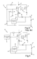
In order to contain costs, it is possible to integrate in one and the same chip (not illustrated) the auxiliary transistor 21 and the main transistor 10. In this case, as shown in FIG. 3, the auxiliary transistor 21 and the main transistor 10 share the drain terminal. The drain terminal is coupled to the internal node 8 (FIG. 1), which is in turn coupled to the primary winding 4 a of the transformer 4, and is at a voltage which is not constant (i.e., which switches between a value of approximately 0 V and the value of the input voltage Vin).
The self-supply circuit 15 of FIG. 3 thus enables charging of the accumulation capacitor 16 only when the main transistor 10 is turned off, i.e., when the voltage of the aforesaid drain terminal (or, in a similar way of the internal node 8) is high and equal to the value of the input voltage Vin. Consequently, in the case where the self-supply circuit 15 is also used for self-supply of the PWM controller 12 through the accumulation capacitor 16 during the switching phase of the PWM controller 12, the current Icharge can charge the accumulation capacitor 16 only during the OFF phase of the switching period, when the voltage of the drain terminal is high. This condition can jeopardize proper operation of the self-supply circuit 15, especially for high values of duty cycle (higher than 50%) of the switching signal that regulates operation of the voltage converter 1, and consequently considerably limits the maximum value of duty cycle that can be obtained.
In fact, the auxiliary transistor 21 should be able to turn on rapidly during turning-off of the main transistor 10 in order to maximize the useful time (substantially corresponding to the OFF phase of the switching signal) for charging the accumulation capacitor 16. However, the switching rate of the auxiliary transistor 21 is limited by the gate capacitance of the latter and by the presence of the first biasing resistor 22, the value of which is commonly chosen high (for example, equal to 15 MΩ) in order to minimize the losses.
In use, when the main transistor 10 is turned on, the voltage on the internal node 8 is approximately 0 V and the auxiliary transistor 21 is off. When the main transistor 10 is turned off, the signal Vcc OK generated by the control logic 28 controls opening of the switch 26, the voltage on the drain terminal of the auxiliary transistor 21 starts to increase, and the gate capacitor of the same auxiliary transistor 21 is charged, first by the injection of charge coming from the capacitance between the drain and gate terminals and then, when the voltage on the drain terminal reaches a sufficiently high value, through the biasing resistor 22. Both of these contributions of charge may not be, however, sufficient to turn on the auxiliary transistor 21 completely, and to supply the current Icharge required by the current generator 24, in a reasonable time. Consequently, a substantial part of the time available for charging the accumulation capacitor 16 may not be exploited. Therefore, in order to guarantee in any case the self-supply operation, it is hence common to limit the duty cycle to a value lower than 50%, for example equal to 45%.
SUMMARY
Embodiments of the present disclosure include a self-supply circuit and method that will be free from the drawbacks described above, and in particular that will enable self-supply to be guaranteed in a voltage converter without setting any limitations on the duty cycle.
BRIEF DESCRIPTION OF THE DRAWINGS
One or more embodiments of the disclosure are now described, purely by way of non-limiting example and with reference to the attached drawings, wherein:
FIG. 1 shows a circuit diagram of a flyback voltage converter of a known type;
FIG. 2 shows a circuit diagram of a self-supply circuit of the voltage converter of FIG. 1;
FIG. 3 shows a different circuit diagram, of a known type, of the self-supply circuit;
FIG. 4 shows part of a circuit diagram of a voltage converter with highlighted therein a self-supply circuit, made according to an embodiment of the present disclosure;
FIG. 5 shows a possible circuit embodiment of a precharge stage within the self-supply circuit of FIG. 4;
FIGS. 6 and 7 show the plots in time of the waveforms of electrical signals involved during a precharge step in the voltage converter of FIG. 4;
FIG. 8 shows a possible embodiment of a precharge control block inside the precharge stage of FIG. 5;
FIG. 9 shows the plots of electrical signals involved during the precharge step;
FIG. 10 shows a first embodiment of a portion of the precharge-control block;
FIG. 11 shows the plots of the signals involved during the precharge step, using the precharge control block of FIG. 10;
FIG. 12 shows a second embodiment of the precharge control block;
FIG. 13 shows the plots of the signals involved during the precharge step, using the precharge control block of FIG. 12;
FIG. 14 shows a third embodiment of the precharge control block; and
FIG. 15 shows the plots of the signals involved during the precharge step, using the precharge control block of FIG. 14.
DETAILED DESCRIPTION
FIG. 4 shows a self-supply circuit 30, made according to an embodiment of the present disclosure. Elements that have already been described with reference to the known art are designated by the same reference numbers and are not described again. In particular, the self-supply circuit 30 may find use in a voltage converter 1 of the type described with reference to FIG. 1 (not illustrated in FIG. 4).
In detail, the self-supply circuit 30 differs from the one described in FIG. 3, in so far as it comprises a precharge stage 31 coupled (in this embodiment coupled) directly to the gate terminal of the auxiliary transistor 21. In particular, it should be noted that, even though they are not described again in detail, the second biasing resistor 23 and the control logic 28 are present (for greater clarity, these elements are not shown again in the subsequent figures).
The precharge stage 31 enables a rapid switching of the auxiliary transistor 21 to be obtained during each switching cycle, in so far as it has the function of precharging the capacitance between the gate and source terminals of the auxiliary transistor 21, whilst the voltage on the drain terminal is still at a low value, during or at the end of the turning-on phase (ON phase of the switching period) of the main transistor 10. In this way, following upon turning-off of the main transistor 10, when the voltage present on the internal node 8 starts to increase, the auxiliary transistor 21 is already turned on, and the current generator 24 can generate the current Icharge for charging the accumulation capacitor 16 without appreciable time delays. It should be noted that the precharge stage 31 has also the function of controlling turning-off of the auxiliary transistor 21 in order to interrupt the flow of the current Icharge.
In particular, the value of the current Icharge generated by the current generator 24 is determined as a function of the maximum duty cycle Dmax of the switching signal, and of the current consumption Icons of the voltage converter 1, and must satisfy the following condition:
I charge > I cons 1 - D max
When this relation is satisfied, the self-supply operation is carried out without limiting the duty cycle of the switching signal.
In fact, the average charge current of the accumulation capacitor 16 is
I average =I charge ·D aux
where Daux is the duty-cycle of the current Icharge, i.e., the ratio between the time used for charging the accumulation capacitor 16 and the switching period. Since, as discussed previously, charging of the accumulation capacitor 16 is enabled when the main transistor is turned off we have:
D aux=1−D max
The average current Iaverage is such as to charge the accumulation capacitor 16 and simultaneously sustain the consumption of the PWM controller 12. Consequently, in order for this to occur, the following expression (wherefrom the aforesaid condition derives) holds:
I average=(1−D maxI charge >I cons
As shown in FIG. 5, in a possible embodiment, the precharge stage 31 comprises: a first precharge switch 33, coupled between the gate terminal of the auxiliary transistor 21 and the reference terminal 9; a second precharge switch 34, coupled between the source terminal of the auxiliary transistor 21 and the reference terminal 9; a third precharge switch 35, coupled between the gate terminal of the auxiliary transistor 21 and the supply terminal 13 of the PWM controller 12 (and hence to the accumulation capacitor 16); and a precharge control block 36, designed to generate respective control signals for the first, second, and third precharge switches 33, 34, 35 such as to implement self-supply management. In detail, the first precharge switch 33 is controlled in opening and closing by a logic signal HV_EN_G, the second precharge switch 34 is controlled in opening and closing by a logic signal HV_EN_S, and the third precharge switch 35 is controlled in opening and closing by a logic signal EN_PRE.
In particular, when the current generator 24 is disabled (during the ON phase of the switching period of the main transistor 10), the first and second precharge switches 33, 34 are closed (signals HV_EN_G and HV_EN_S high), and the third precharge switch 35 is open (signal EN_PRE low), thus connecting the source and gate terminals of the auxiliary transistor 21 to the reference terminal 9. At the end of the ON phase of switching of the main transistor 10 (as will be clarified hereinafter), the first precharge switch 33 is controlled in opening (signal HV_EN_G low), whilst the second and third precharge switches 34, 35 are controlled in closing (signals HV_EN_S and EN_PRE high). In this way, the source terminal of the auxiliary transistor 21 is coupled to the reference terminal 9, and the gate terminal directly to the supply voltage Vcc, thus starting precharging of the gate-source capacitance of the auxiliary transistor 21 to the supply voltage Vcc.
Before the voltage on the drain terminal of the auxiliary transistor 21 starts to increase, or at the moment in which the same voltage starts to increase, the second and third precharge switches 34, 35 are controlled in opening (signals HV_EN_S and EN_PRE low), given that the precharging phase can be considered completed. It should be noted that the auxiliary transistor 21, in this situation, is already turned on, and the charge current Icharge can immediately flow (as soon as the voltage at the internal node 8 becomes high) through the current generator 24, thus charging the accumulation capacitor 16 so that the entire OFF phase of the switching signal is exploited.
FIG. 6 shows the waveforms of the voltage on the drain terminal, designated by V(drain), on the gate terminal, designated by V(gate), and on the source terminal, designated by V(source), of the auxiliary transistor 21, and of the charge current Icharge. Following the switching of the main transistor 10 (instant of times t1 and t2), the waveform of the current Icharge follows the waveform of the voltage on the drain terminal V(drain), responding substantially immediately to its variations, thanks to the precharging phase managed by the precharge stage 31.
FIG. 7 shows an enlarged portion of the aforesaid waveforms, approximately upon switching at the instant of time t2, together with the plot of the logic signals HV_EN_G, HV_EN_S, and EN_PRE, with highlighted the precharging phase. It should be noted that the voltage on the gate terminal V(gate) starts to rise after switching of the signal EN_PRE to the high value, as a result of the precharging operation.
FIG. 8 shows a possible embodiment of the precharge-control block 36 of the precharge stage 31, which comprises a precharge logic 38, and an end-of-precharge controller 39.
The end-of-precharge controller 39 controls, as will be described in detail hereinafter, the appropriate instant of time at which the precharging phase of the auxiliary transistor 21 stops, generating an end-of-precharge signal END_PRE.
The precharge logic 38 receives at input, from the end-of-precharge controller 39, the end-of-precharge signal END_PRE, and, from the PWM controller 12, a control signal QG, which is a function of a signal that controls, in a per-se known manner (for example, through a driver), the main transistor 10. The precharge logic 38, according to the end-of-precharge signal END_PRE and to the control signal QG, generates the logic signals HV_EN_G, HV_EN_S, EN_PRE for management of the precharging phase.
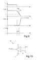
FIG. 9 shows in detail the plots of the control signal QG, of the logic signal EN_PRE, of the voltage on the gate terminal V(gate) and of the voltage on the drain terminal V(drain) of the main transistor 10. In detail, when the control signal QG is active high, the main transistor 10 is in conduction (the voltage signal on the gate terminal V(gate) is high), whilst the voltage signal on the drain terminal V(drain) and the logic signal EN_PRE have a low value, indicating that the precharging phase has not started yet. As soon as the signal QG assumes a low value (instant of time t1), the turning-off transient of the main transistor 10 starts, the voltage signal on the gate terminal V(gate) starts to decrease, and the logic signal EN_PRE assumes a high value, indicating the start of the precharging interval. The precharging phase is disabled by the end-of-precharge controller 39 at the instant of time t2, before or at the end of a delay interval Tdelay that represents a delay of turning-off of the main transistor 10, after which the voltage signal on the gate terminal V(gate) drops below the threshold voltage VTH of the main transistor 10, and the voltage on the drain terminal V(drain) starts to increase. It is in fact expedient for the precharging phase to terminate before the voltage signal on the drain terminal V(drain) starts to increase so as to prevent the phenomenon of cross-conduction between the drain terminal of the auxiliary transistor 21 and the reference terminal 9.
As is shown in FIG. 10, in a first embodiment, the end-of-precharge controller, here designated by 39′, includes a comparator device 42, which receives on a first input a reference voltage VREF, and on a second input the voltage on the gate terminal V(gate) taken on the gate terminal of the main transistor 10, and supplies at output the end-of-precharge signal END_PRE. When the value of the voltage on the gate terminal V(gate) drops below the value of the reference voltage VREF, the end-of-precharge signal END_PRE assumes a logic value (for example, high) indicating the end of the precharging interval.
As is shown in FIG. 11, the value of the reference voltage VREF may be chosen so as to be higher than the threshold-voltage value VTH of the main transistor 10, given that the voltage on the drain terminal V(drain) starts to increase when the voltage on the gate terminal V(gate) drops below the threshold-voltage value VTH.
A second embodiment of the end-of-precharge controller, designated by 39″, is shown in FIG. 12. The end-of-precharge controller 39″ comprises in this case a pulse generator 44, which receives on an input thereof the control signal QG, and generates at output the end-of-precharge signal END_PRE, here of an impulsive type, for example, having a pulse duration Tpulse equal to or shorter than the delay interval Tdelay.
As is shown in FIG. 13, the end-of-precharge controller 39″ is configured to generate the end-of-precharge signal END_PRE when the control signal QG assumes a low value. In addition, the precharge is stopped (the logic signal EN_PRE is brought to the low value) at the falling edge of the end-of-precharge signal END_PRE.
FIG. 14 shows a third embodiment of the end-of-precharge controller, designated by 39′″, in the case where the PWM controller 12 drives the main transistor 10 in such a way as to guarantee the so-called “soft-switching”. In this embodiment, the end-of-precharge controller 39′″ comprises: a negative-derivative detector (NDD) 45, of a known type and not described in detail, which receives on an input thereof the voltage on the gate terminal V(gate) and supplies on an output thereof a negative-derivative signal NEG_DER, as a function of the sign of the derivative of the voltage on the gate terminal; and a counter block 48, which receives at input the negative-derivative signal NEG_DER and supplies on an output thereof the end-of-precharge signal END_PRE.
In detail, and as is shown in FIG. 15, at an instant t1, the control signal QG switches from the high level to the low level, controlling turning-off of the main transistor 10. At the same instant, the logic signal EN_PRE assumes a high value, indicating start of the precharging interval. Next, at an instant t2, the voltage on the gate terminal V(gate) starts to decrease and the negative-derivative signal NEG_DER assumes a high value, indicating that the derivative of the signal has assumed a negative value. At an instant t3, on account of the Miller effect, the voltage on the gate terminal V(gate) assumes a stationary value. Approximately at the same instant of time t3, the negative-derivative signal NEG_DER returns to the low value, and the voltage on the drain terminal V(drain) starts to increase slowly. When the Miller effect terminates (instant of time t4), the voltage on the gate terminal V(gate) starts to decrease again, the voltage on the drain terminal V(drain) increases rapidly, and a new rising edge of the negative-derivative signal NEG_DER determines the end of the precharging interval (the logic signal EN_PRE assumes a low value). In particular, the counter block 48 detects the occurrence of the second pulse generated by the negative-derivative detector 45, and consequently generates the end-of-precharge signal END_PRE.
The above-described embodiments, as well as other embodiments, of a self-supply circuit and method for a voltage converter may allow a number of advantages to be achieved.
In particular, precharging of the gate terminal of the auxiliary transistor 21 that manages the precharging phase enables maximization of the time interval useful for charging the accumulation capacitor 16, so as to guarantee proper self-supply of the controller 12 of the voltage converter 1 without imposing limitations on the duty cycle of the switching signal. In fact, thanks to the preceding precharging phase, following turning-off of the main transistor 10, the auxiliary transistor 21 is already turned on and the current generator 24 can supply the current Icharge to the accumulation capacitor 16 without appreciable time delays (after the main transistor is turned off).
Finally, it is clear that modifications and variations can be made to what is described and illustrated herein, without thereby departing from the scope of the present disclosure.
In particular, it is clear that, even though the embodiments have been described with particular reference to a configuration of a flyback type, these other embodiments may be applied in all converters (or regulators, or power supplies) operating in switched-mode (the so-called SMPS—Switch-Mode Power Supply).
In addition, the embodiments described above, as well as other embodiments, may be used irrespective of: the modality of energy transfer between the source and load, at a fixed or variable frequency; the particular circuit solution used for implementing operation of the individual blocks of the control circuit; the type of control switch; and the feedback mode envisaged on the primary side of the transformer.
Furthermore, one or both of Tdelay and Tpulse may extend to or beyond a time when V(gate) of the main transistor 10 equals VTH of the main transistor.
Moreover, some or all of the components in the circuits of FIGS. 1-5, 8, 10, 12, and 14 may be discrete components, disposed on the same integrated circuit (IC) as others of the components, or disposed on ICs that are different from ICs on which others of the components are disposed.
Naturally, in order to satisfy local and specific requirements, a person skilled in the art may apply to the solution described above many modifications and alterations. Particularly, although the present disclosure has been described with a certain degree of particularity with reference to described embodiment(s) thereof, it should be understood that various omissions, substitutions and changes in the form and details as well as other embodiments are possible. Moreover, it is expressly intended that specific elements and/or method steps described in connection with any disclosed embodiment of the disclosure may be incorporated in any other embodiment as a general matter of design choice.

Claims (6)

1. A self-supply circuit, for a voltage converter having a main switch and a controller, designed to control switching of said main switch for controlling an output voltage, said self-supply circuit comprising:
a charge accumulator, coupled to said controller and designed to supply a self-supply voltage to said controller;
a generator, operable to supply a charge current to said charge accumulator; and
a charge switching circuit, operable to control transfer of said charge current to said charge accumulator, and
a precharge stage, coupled to said charge switching circuit and configured to carry out precharging of an intrinsic capacitance of said charge switching circuit, before a turning-off transient of said main switch ends;
wherein said charge switching circuit comprises an auxiliary transistor having a gate terminal coupled to said precharge stage, and a second conduction terminal coupled to said generator, and said precharge stage comprises a precharge controller and precharge switching circuit; said precharge controller being configured to control said precharge switching circuit for supplying said self-supply voltage to said gate terminal during said precharging; and
wherein said precharge switching circuit comprises a first switch, coupled between said second conduction terminal and a reference potential, and a second switch, coupled between said gate terminal and said charge-accumulator; said precharge controller being designed to close said first switch and second switch during said precharging.
2. The circuit according to claim 1, wherein said precharge switching circuit comprises a third switch, coupled between said gate terminal and said reference potential; said precharge controller being designed to open said first switch and second switch at the end of said precharging.
3. A self-supply circuit, for a voltage converter having a main switch and a controller, designed to control switching of said main switch for controlling an output voltage, said self-supply circuit comprising:
a charge accumulator, coupled to said controller and designed to supply a self-supply voltage to said controller;
a generator, operable to supply a charge current to said charge accumulator means; and
a charge switching circuit, operable to control transfer of said charge current to said charge accumulator means, and
a precharge stage, coupled to said charge switching circuit and configured to carry out precharging of an intrinsic capacitance of said charge switching circuit, before a turning-off transient of said main switch ends;
wherein said precharge stage comprises a precharge controller and precharge switching means, and said precharge controller comprises a precharge logic block and an end-of-precharge controller block; said end-of-precharge controller block being configured to generate an end-of-precharge signal, and said precharge logic block being designed to control said precharge switching circuit so as to stop said precharging, when said end-of-precharge signal assumes a given value; and
wherein said end-of-precharge controller block comprises a comparator device, designed to receive on a first input a reference signal and on a second input a voltage signal present on a control terminal of said main switch, and to generate at output said end-of-precharge signal; said reference signal having a value greater than or equal to a threshold conduction voltage of said main switch.
4. A self-supply circuit, for a voltage converter having a main switch and a controller, designed to control switching of said main switch for controlling an output voltage, said self-supply circuit comprising:
a charge accumulator, coupled to said controller and designed to supply a self-supply voltage to said controller;
a generator, operable to supply a charge current to said charge accumulator means; and
a charge switching circuit, operable to control transfer of said charge current to said charge accumulator means, and
a precharge stage, coupled to said charge switching circuit and configured to carry out precharging of an intrinsic capacitance of said charge switching circuit, before a turning-off transient of said main switch ends;
wherein said precharge stage comprises a precharge controller and precharge switching means, and said precharge controller comprises a precharge logic block and an end-of-precharge controller block; said end-of-precharge controller block being configured to generate an end-of-precharge signal, and said precharge logic block being designed to control said precharge switching circuit so as to stop said precharging, when said end-of-precharge signal assumes a given value; and
wherein said charge switching circuit comprises an auxiliary transistor having a first conduction terminal coupled to a respective conduction terminal of said main switch, and, during said turning-off transient, the voltage of said first conduction terminal undergoes an increase from a first value to a second value; and wherein said controller is designed to control switching of said main switch as a function of a driving signal, and said end-of-precharge controller block comprises a pulse-generator device, which receives at input said driving signal and generates at output said end-of-precharge signal based on said driving signal; said end-of-precharge signal being a pulse having a duration shorter than a time interval comprised between an instant of turning-off of said main switch and an instant of start of said increase.
5. A self-supply circuit, for a voltage converter having a main switch and a controller, designed to control switching of said main switch for controlling an output voltage, said self-supply circuit comprising:
a charge accumulator, coupled to said controller and designed to supply a self-supply voltage to said controller;
a generator, operable to supply a charge current to said charge accumulator means; and
a charge switching circuit, operable to control transfer of said charge current to said charge accumulator means, and
a precharge stage, coupled to said charge switching circuit and configured to carry out precharging of an intrinsic capacitance of said charge switching circuit, before a turning-off transient of said main switch ends;
wherein said precharge stage comprises a precharge controller and precharge switching means, and said precharge controller comprises a precharge logic block and an end-of-precharge controller block; said end-of-precharge controller block being configured to generate an end-of-precharge signal, and said precharge logic block being designed to control said precharge switching circuit so as to stop said precharging, when said end-of-precharge signal assumes a given value; and
wherein said end-of-precharge controller block comprises a derivative-detecting device and a counter device, coupled to said derivative-detecting device; said derivative-detecting device being designed to receive at input a voltage signal present on a control terminal of said main switch and to generate at output a negative-derivative signal in the presence of a decrease of said voltage signal, and said counter device being designed to generate at output said end-of-precharge signal as a function of said negative-derivative signal.
6. A power supply, comprising:
an input node operable to receive an input signal;
an output node operable to provide a supply signal having a supply level;
a first switch coupled between the input and output nodes and including a control node having an associated capacitance;
a controller operable to enable a current to flow through the switch from the input node to the output node while the input signal has a first signal level; and a precharger operable to charge the capacitance while the input signal has a second signal level, a magnitude of the second signal level being less than a magnitude of the first signal level;
wherein:
the precharger comprises a second switch that is coupled between the control node of the first switch and the output node; and
the precharger is operable to charge the capacitance by closing the second switch.
US12/324,548 2007-11-29 2008-11-26 Self-supply circuit and method for a voltage converter Active 2031-06-09 US8325502B2 (en)

Applications Claiming Priority (3)

Application Number Priority Date Filing Date Title
IT000860A ITTO20070860A1 (en) 2007-11-29 2007-11-29 CIRCUIT AND ITS SELF-POWER SUPPLY METHOD FOR A VOLTAGE CONVERTER
ITTO2007A000860 2007-11-29
ITTO2007A0860 2007-11-29

Publications (2)

Publication Number Publication Date
US20090140712A1 US20090140712A1 (en) 2009-06-04
US8325502B2 true US8325502B2 (en) 2012-12-04

Family

ID=40315046

Family Applications (1)

Application Number Title Priority Date Filing Date
US12/324,548 Active 2031-06-09 US8325502B2 (en) 2007-11-29 2008-11-26 Self-supply circuit and method for a voltage converter

Country Status (4)

Country Link
US (1) US8325502B2 (en)
EP (1) EP2066012B1 (en)
CN (1) CN101483391B (en)
IT (1) ITTO20070860A1 (en)

Cited By (7)

* Cited by examiner, † Cited by third party
Publication number Priority date Publication date Assignee Title
US20120025608A1 (en) * 2010-07-30 2012-02-02 Melanson John L Multiple power sources for a switching power converter controller
US20120119676A1 (en) * 2010-11-15 2012-05-17 Power Integrations, Inc. Flyback power converter with divided energy transfer element
US9161401B1 (en) 2014-03-20 2015-10-13 Cirrus Logic, Inc. LED (light-emitting diode) string derived controller power supply
US9484832B2 (en) 2011-12-14 2016-11-01 Koninklijke Philips N.V. Isolation of secondary transformer winding current during auxiliary power supply generation
US20180006559A1 (en) * 2016-07-01 2018-01-04 Texas Instruments Incorporated Reducing Voltage Rating of Devices in a Multilevel Converter
US10256723B1 (en) * 2018-07-25 2019-04-09 Texas Instruments Incorporated Integrated circuit feed forward circuit with translinear cell
US12334159B2 (en) 2019-07-11 2025-06-17 Samsung Electronics Co., Ltd. Method and circuit for providing auxiliary power and storage device including the same

Families Citing this family (14)

* Cited by examiner, † Cited by third party
Publication number Priority date Publication date Assignee Title
ITTO20070862A1 (en) * 2007-11-29 2009-05-30 St Microelectronics Srl VOLTAGE ISOLATED CONVERTER WITH FEEDBACK TO THE PRIMARY AND PASSIVE SNUBBER NETWORK, AND RELATIVE CONTROL METHOD
ITTO20070859A1 (en) * 2007-11-29 2009-05-30 St Microelectronics Srl VOLTAGE ISOLATED CONVERTER WITH FEEDBACK TO THE PRIMARY, AND RELATIVE OUTPUT TENSION CONTROL METHOD
US20110157919A1 (en) * 2009-12-30 2011-06-30 Yeshoda Yedevelly Vcc generator for switching regulator
US9343971B2 (en) * 2009-12-30 2016-05-17 Silicon Laboratories Inc. Synchronous VCC generator for switching voltage regulator
US8519686B2 (en) * 2010-05-19 2013-08-27 Hamilton Sundstrand Corporation SSPC for soft start of DC link capacitor
JP2014503168A (en) * 2011-01-24 2014-02-06 サンサン ライティング チャイナ カンパニー リミテッド Low voltage control power supply circuit and drive control method thereof
EP2525492B1 (en) * 2011-05-19 2019-07-10 Nxp B.V. Electronic switching device
TWI431909B (en) * 2011-10-04 2014-03-21 Delta Electronics Inc Power supply
CN102931846B (en) * 2012-09-18 2015-08-26 深圳市力生美半导体器件有限公司 Power module circuit, power switch chip, Switching Power Supply and method for designing thereof
CN105657949A (en) * 2014-11-13 2016-06-08 广东雪莱特光电科技股份有限公司 Negative voltage rectification circuit and high strength gas discharge lamp
US9716439B2 (en) 2015-01-30 2017-07-25 Infineon Technologies Austria Ag Self supply for synchronous rectifiers
CN108964465B (en) * 2017-05-26 2023-07-04 富满微电子集团股份有限公司 Power converter with self-powered control mechanism
CN109713906A (en) * 2018-12-30 2019-05-03 杭州中恒电气股份有限公司 A kind of controlled resonant converter
CN114050711B (en) * 2021-11-16 2022-09-13 东科半导体(安徽)股份有限公司 Self-powered method for detecting current of built-in high-voltage power tube

Citations (34)

* Cited by examiner, † Cited by third party
Publication number Priority date Publication date Assignee Title
US4975823A (en) 1987-09-30 1990-12-04 Deutsche Thomson-Brandt Gmbh Switched power supply with current mode regulation
US5783962A (en) * 1995-07-06 1998-07-21 Siemens Aktiengesellschaft Bootstrap circuit and integrated memory circuit having the bootstrap circuit
US5874841A (en) 1997-07-28 1999-02-23 Philips Electronics North America Corporation Sample-and-hold circuit for a switched-mode power supply
US5978241A (en) 1999-01-28 1999-11-02 Industrial Technology Research Institute Wide-linear range tunable transconductor using MOS
US5982640A (en) 1998-02-03 1999-11-09 Philips Electronics North America Corporation Arrangement for reducing the effects of capacitive coupling in a control circuit for a switched-mode power supply
US6011414A (en) 1998-02-03 2000-01-04 Philips Electronics North America Corporation Arrangement for reducing the effects of capacitive coupling in a control circuit for a switched-mode power supply
US6122180A (en) 1998-12-18 2000-09-19 Fairfield Korea Semiconductor Ltd. SMPS with constant power control circuit
US20010033501A1 (en) * 1999-06-25 2001-10-25 Nebrigic Dragan Danilo Progressive start-up circuit for activating a charge pump
US20010033498A1 (en) 2000-04-25 2001-10-25 Samsung Electro-Mechanics Co., Ltd. High efficiency converter for zero voltage switching
US6445598B1 (en) 1999-12-09 2002-09-03 Sanken Electric Co., Ltd. Dc-dc converter
US20030001548A1 (en) 2000-01-14 2003-01-02 Martin Feldtkeller Circuit configuration for applying a supply voltage to a load and method for such application
US20030206425A1 (en) 2002-04-03 2003-11-06 International Rectifier Corporation Synchronous buck converter with improved transient performance
US20040080962A1 (en) 2002-10-24 2004-04-29 Arthur Charych Apparatus and method for DC/DC converter having high speed and accuracy
US20040257839A1 (en) 2003-06-18 2004-12-23 Ta-Yung Yang Primary-side regulated pulse width modulation controller with improved load regulation
US20050073862A1 (en) 2003-10-02 2005-04-07 Alexander Mednik Switching power converter and method of controlling output voltage thereof using predictive sensing of magnetic flux
US6894910B1 (en) 2003-03-03 2005-05-17 Lockheed Martin Corporation Dynamic duty cycle clamping for switching converters
US6990000B1 (en) 2004-09-17 2006-01-24 Iwatt Inc. Reconstruction of the output voltage of an AC-DC power converter
US20060050539A1 (en) 2004-09-09 2006-03-09 Ta-Yung Yang Switching control circuit with variable switching frequency for primary-side-controlled power converters
US20060152951A1 (en) 2002-07-19 2006-07-13 Mauro Fagnani Bootstrap circuit for switching power supplies
CN1826720A (en) 2003-07-28 2006-08-30 崇贸科技股份有限公司 Primary-Side Controlled Flyback Power Converter
US20060209571A1 (en) 2005-02-25 2006-09-21 Sanken Electric Co., Ltd. DC converter
CN1848641A (en) 2005-03-10 2006-10-18 三洋电机株式会社 Quasi resonant type switching power supply unit and quasi resonant type switching power apparatus using the same
US20060250824A1 (en) 2005-05-09 2006-11-09 Wekhande Shashank S Capacitor charging methods and apparatus
US20070047269A1 (en) * 2005-08-31 2007-03-01 Matsushita Electric Industrial Co., Ltd. Output voltage detection circuit, isolated switching power supply, and semiconductor device
CN1937379A (en) 2006-09-18 2007-03-28 崇贸科技股份有限公司 Linear predictive sampling circuit and device for measuring degaussing voltage of transformer
US20080104432A1 (en) * 2006-10-30 2008-05-01 Quantance, Inc. Power combining power supply system
US20090086513A1 (en) 2007-09-28 2009-04-02 Stmicroelectronics S.R.L. Control method and device for switching power supplies
US7525819B2 (en) * 2005-03-02 2009-04-28 Fairchild Korea Semiconductor, Ltd. Switching mode power supply and method for generating a bias voltage
US20090141520A1 (en) 2007-11-29 2009-06-04 Stmicroelectronics S.R.L. Isolated voltage converter with feedback on the primary winding, and corresponding method for controlling the output voltage
US7545657B2 (en) * 2006-08-28 2009-06-09 Sanken Electric Co., Ltd. Switching power source apparatus
US20090147546A1 (en) 2007-11-29 2009-06-11 Stmicroelectronics S.R.L. Isolated voltage converter with feedback on the primary winding and passive snubber network, and corresponding control method
US7561446B1 (en) 2005-09-15 2009-07-14 Vlt, Inc. Double-clamped ZVS buck-boost power converter
US7719860B2 (en) * 2003-07-15 2010-05-18 Sanken Electric Co., Ltd. Power supply and its controlling method
US7859859B2 (en) 2006-11-20 2010-12-28 Picor Corporation Primary side sampled feedback control in power converters

Family Cites Families (1)

* Cited by examiner, † Cited by third party
Publication number Priority date Publication date Assignee Title
CN2699577Y (en) * 2003-11-06 2005-05-11 李希珍 Isolating driver for insulated gate power tube

Patent Citations (35)

* Cited by examiner, † Cited by third party
Publication number Priority date Publication date Assignee Title
US4975823A (en) 1987-09-30 1990-12-04 Deutsche Thomson-Brandt Gmbh Switched power supply with current mode regulation
US5783962A (en) * 1995-07-06 1998-07-21 Siemens Aktiengesellschaft Bootstrap circuit and integrated memory circuit having the bootstrap circuit
US5874841A (en) 1997-07-28 1999-02-23 Philips Electronics North America Corporation Sample-and-hold circuit for a switched-mode power supply
US5982640A (en) 1998-02-03 1999-11-09 Philips Electronics North America Corporation Arrangement for reducing the effects of capacitive coupling in a control circuit for a switched-mode power supply
US6011414A (en) 1998-02-03 2000-01-04 Philips Electronics North America Corporation Arrangement for reducing the effects of capacitive coupling in a control circuit for a switched-mode power supply
US6122180A (en) 1998-12-18 2000-09-19 Fairfield Korea Semiconductor Ltd. SMPS with constant power control circuit
US5978241A (en) 1999-01-28 1999-11-02 Industrial Technology Research Institute Wide-linear range tunable transconductor using MOS
US20010033501A1 (en) * 1999-06-25 2001-10-25 Nebrigic Dragan Danilo Progressive start-up circuit for activating a charge pump
US6445598B1 (en) 1999-12-09 2002-09-03 Sanken Electric Co., Ltd. Dc-dc converter
US20030001548A1 (en) 2000-01-14 2003-01-02 Martin Feldtkeller Circuit configuration for applying a supply voltage to a load and method for such application
US20010033498A1 (en) 2000-04-25 2001-10-25 Samsung Electro-Mechanics Co., Ltd. High efficiency converter for zero voltage switching
US20030206425A1 (en) 2002-04-03 2003-11-06 International Rectifier Corporation Synchronous buck converter with improved transient performance
US20060152951A1 (en) 2002-07-19 2006-07-13 Mauro Fagnani Bootstrap circuit for switching power supplies
US20040080962A1 (en) 2002-10-24 2004-04-29 Arthur Charych Apparatus and method for DC/DC converter having high speed and accuracy
US6894910B1 (en) 2003-03-03 2005-05-17 Lockheed Martin Corporation Dynamic duty cycle clamping for switching converters
US20040257839A1 (en) 2003-06-18 2004-12-23 Ta-Yung Yang Primary-side regulated pulse width modulation controller with improved load regulation
US7719860B2 (en) * 2003-07-15 2010-05-18 Sanken Electric Co., Ltd. Power supply and its controlling method
CN1826720A (en) 2003-07-28 2006-08-30 崇贸科技股份有限公司 Primary-Side Controlled Flyback Power Converter
US20050073862A1 (en) 2003-10-02 2005-04-07 Alexander Mednik Switching power converter and method of controlling output voltage thereof using predictive sensing of magnetic flux
US20060050539A1 (en) 2004-09-09 2006-03-09 Ta-Yung Yang Switching control circuit with variable switching frequency for primary-side-controlled power converters
US6990000B1 (en) 2004-09-17 2006-01-24 Iwatt Inc. Reconstruction of the output voltage of an AC-DC power converter
US20060209571A1 (en) 2005-02-25 2006-09-21 Sanken Electric Co., Ltd. DC converter
US7525819B2 (en) * 2005-03-02 2009-04-28 Fairchild Korea Semiconductor, Ltd. Switching mode power supply and method for generating a bias voltage
CN1848641A (en) 2005-03-10 2006-10-18 三洋电机株式会社 Quasi resonant type switching power supply unit and quasi resonant type switching power apparatus using the same
US20060250824A1 (en) 2005-05-09 2006-11-09 Wekhande Shashank S Capacitor charging methods and apparatus
US20070047269A1 (en) * 2005-08-31 2007-03-01 Matsushita Electric Industrial Co., Ltd. Output voltage detection circuit, isolated switching power supply, and semiconductor device
US7561446B1 (en) 2005-09-15 2009-07-14 Vlt, Inc. Double-clamped ZVS buck-boost power converter
US7545657B2 (en) * 2006-08-28 2009-06-09 Sanken Electric Co., Ltd. Switching power source apparatus
CN1937379A (en) 2006-09-18 2007-03-28 崇贸科技股份有限公司 Linear predictive sampling circuit and device for measuring degaussing voltage of transformer
US20080104432A1 (en) * 2006-10-30 2008-05-01 Quantance, Inc. Power combining power supply system
US7859859B2 (en) 2006-11-20 2010-12-28 Picor Corporation Primary side sampled feedback control in power converters
US20090086513A1 (en) 2007-09-28 2009-04-02 Stmicroelectronics S.R.L. Control method and device for switching power supplies
US20090141520A1 (en) 2007-11-29 2009-06-04 Stmicroelectronics S.R.L. Isolated voltage converter with feedback on the primary winding, and corresponding method for controlling the output voltage
US20090147546A1 (en) 2007-11-29 2009-06-11 Stmicroelectronics S.R.L. Isolated voltage converter with feedback on the primary winding and passive snubber network, and corresponding control method
US20090175057A1 (en) 2007-11-29 2009-07-09 Stmicroelectronics S.R.L. Isolated voltage converter with feedback on the primary winding, and corresponding method for controlling the output voltage

Non-Patent Citations (2)

* Cited by examiner, † Cited by third party
Title
CN 200810246381.6; State Intellectual Property Office of People's Republic of China Search Report, Dated Jul. 23, 2012.
European Search Report for European Application No. EP08170303, European Patent Office, Munich, Oct. 18, 2010, pp. 3.

Cited By (11)

* Cited by examiner, † Cited by third party
Publication number Priority date Publication date Assignee Title
US20120025608A1 (en) * 2010-07-30 2012-02-02 Melanson John L Multiple power sources for a switching power converter controller
US10263532B2 (en) * 2010-07-30 2019-04-16 Signify Holding B.V. Multiple power sources for a switching power converter controller
US20120119676A1 (en) * 2010-11-15 2012-05-17 Power Integrations, Inc. Flyback power converter with divided energy transfer element
US9484832B2 (en) 2011-12-14 2016-11-01 Koninklijke Philips N.V. Isolation of secondary transformer winding current during auxiliary power supply generation
US10122282B2 (en) 2011-12-14 2018-11-06 Philips Lighting Holding B.V. Isolation of secondary transformer winding current during auxiliary power supply generation
US9161401B1 (en) 2014-03-20 2015-10-13 Cirrus Logic, Inc. LED (light-emitting diode) string derived controller power supply
US9713206B2 (en) 2014-03-20 2017-07-18 Philips Lighting Holding B.V. LED (light-emitting diode) string derived controller power supply
US20180006559A1 (en) * 2016-07-01 2018-01-04 Texas Instruments Incorporated Reducing Voltage Rating of Devices in a Multilevel Converter
US10447158B2 (en) * 2016-07-01 2019-10-15 Texas Instruments Incorporated Reducing voltage rating of devices in a multilevel converter
US10256723B1 (en) * 2018-07-25 2019-04-09 Texas Instruments Incorporated Integrated circuit feed forward circuit with translinear cell
US12334159B2 (en) 2019-07-11 2025-06-17 Samsung Electronics Co., Ltd. Method and circuit for providing auxiliary power and storage device including the same

Also Published As

Publication number Publication date
EP2066012B1 (en) 2014-09-03
ITTO20070860A1 (en) 2009-05-30
CN101483391A (en) 2009-07-15
US20090140712A1 (en) 2009-06-04
CN101483391B (en) 2013-06-19
EP2066012A3 (en) 2010-12-01
EP2066012A2 (en) 2009-06-03

Similar Documents

Publication Publication Date Title
US8325502B2 (en) Self-supply circuit and method for a voltage converter
CN105391298B (en) Dc-dc converter control
US8222882B2 (en) Power supply controller with input voltage compensation for efficiency and maximum power output
US9343971B2 (en) Synchronous VCC generator for switching voltage regulator
US20160233779A1 (en) Soft switching flyback converter
US20090315523A1 (en) Dc-dc converter
US9083251B2 (en) Power controller with pulse skipping
US20090147546A1 (en) Isolated voltage converter with feedback on the primary winding and passive snubber network, and corresponding control method
US11323031B2 (en) Half-bridge driver circuit with a switched capacitor supply voltage for high side drive signal generation
US20110101946A1 (en) Voltage converters
US20070164720A1 (en) Switch-mode power supply controllers
US20110157919A1 (en) Vcc generator for switching regulator
JP2005525069A (en) Power converter
US7501715B2 (en) Multi-output DC-DC converter
US20080049455A1 (en) Forward converter with synchronous rectification
US10536088B2 (en) Switched mode power supply controller
US6661209B2 (en) Leading edge modulator for post regulation of multiple output voltage power supplies
JP7797624B2 (en) Power conversion device and power conversion system
KR100856901B1 (en) Digital Soft-Start Circuits for Pulse Width Modulated Signal Generators and Switching-Mode Power Supplies Containing the Same
US10644688B2 (en) Biasing circuit for switch
CN115622407A (en) High-side synchronous rectifier drive with reduced controller power supply charging loss and reduced electromagnetic interference
US20260039197A1 (en) Power supply control device, switching power supply, and electronic apparatus
US10892755B2 (en) Driver circuitry for fast, efficient state transitions
US8324874B2 (en) System and method for controlling synchronous switch for a synchronous converter

Legal Events

Date Code Title Description
AS Assignment

Owner name: STMICROELECTRONICS S.R.L., ITALY

Free format text: ASSIGNMENT OF ASSIGNORS INTEREST;ASSIGNORS:GIOMBANCO, SALVATORE;TUMMINARO, SALVATORE;REEL/FRAME:021899/0945

Effective date: 20081124

STCF Information on status: patent grant

Free format text: PATENTED CASE

FPAY Fee payment

Year of fee payment: 4

MAFP Maintenance fee payment

Free format text: PAYMENT OF MAINTENANCE FEE, 8TH YEAR, LARGE ENTITY (ORIGINAL EVENT CODE: M1552); ENTITY STATUS OF PATENT OWNER: LARGE ENTITY

Year of fee payment: 8

MAFP Maintenance fee payment

Free format text: PAYMENT OF MAINTENANCE FEE, 12TH YEAR, LARGE ENTITY (ORIGINAL EVENT CODE: M1553); ENTITY STATUS OF PATENT OWNER: LARGE ENTITY

Year of fee payment: 12