US8314378B2 - Apparatus and method for manufacturing light source device - Google Patents
Apparatus and method for manufacturing light source device Download PDFInfo
- Publication number
- US8314378B2 US8314378B2 US12/782,745 US78274510A US8314378B2 US 8314378 B2 US8314378 B2 US 8314378B2 US 78274510 A US78274510 A US 78274510A US 8314378 B2 US8314378 B2 US 8314378B2
- Authority
- US
- United States
- Prior art keywords
- laser
- light
- stage
- wavelength converting
- amount
- Prior art date
- Legal status (The legal status is an assumption and is not a legal conclusion. Google has not performed a legal analysis and makes no representation as to the accuracy of the status listed.)
- Expired - Fee Related, expires
Links
Images


Classifications
-
- H—ELECTRICITY
- H01—ELECTRIC ELEMENTS
- H01S—DEVICES USING THE PROCESS OF LIGHT AMPLIFICATION BY STIMULATED EMISSION OF RADIATION [LASER] TO AMPLIFY OR GENERATE LIGHT; DEVICES USING STIMULATED EMISSION OF ELECTROMAGNETIC RADIATION IN WAVE RANGES OTHER THAN OPTICAL
- H01S3/00—Lasers, i.e. devices using stimulated emission of electromagnetic radiation in the infrared, visible or ultraviolet wave range
- H01S3/0014—Monitoring arrangements not otherwise provided for
-
- H—ELECTRICITY
- H01—ELECTRIC ELEMENTS
- H01S—DEVICES USING THE PROCESS OF LIGHT AMPLIFICATION BY STIMULATED EMISSION OF RADIATION [LASER] TO AMPLIFY OR GENERATE LIGHT; DEVICES USING STIMULATED EMISSION OF ELECTROMAGNETIC RADIATION IN WAVE RANGES OTHER THAN OPTICAL
- H01S3/00—Lasers, i.e. devices using stimulated emission of electromagnetic radiation in the infrared, visible or ultraviolet wave range
- H01S3/005—Optical devices external to the laser cavity, specially adapted for lasers, e.g. for homogenisation of the beam or for manipulating laser pulses, e.g. pulse shaping
- H01S3/0092—Nonlinear frequency conversion, e.g. second harmonic generation [SHG] or sum- or difference-frequency generation outside the laser cavity
-
- H—ELECTRICITY
- H01—ELECTRIC ELEMENTS
- H01S—DEVICES USING THE PROCESS OF LIGHT AMPLIFICATION BY STIMULATED EMISSION OF RADIATION [LASER] TO AMPLIFY OR GENERATE LIGHT; DEVICES USING STIMULATED EMISSION OF ELECTROMAGNETIC RADIATION IN WAVE RANGES OTHER THAN OPTICAL
- H01S3/00—Lasers, i.e. devices using stimulated emission of electromagnetic radiation in the infrared, visible or ultraviolet wave range
- H01S3/09—Processes or apparatus for excitation, e.g. pumping
- H01S3/091—Processes or apparatus for excitation, e.g. pumping using optical pumping
- H01S3/094—Processes or apparatus for excitation, e.g. pumping using optical pumping by coherent light
- H01S3/094076—Pulsed or modulated pumping
-
- H—ELECTRICITY
- H01—ELECTRIC ELEMENTS
- H01S—DEVICES USING THE PROCESS OF LIGHT AMPLIFICATION BY STIMULATED EMISSION OF RADIATION [LASER] TO AMPLIFY OR GENERATE LIGHT; DEVICES USING STIMULATED EMISSION OF ELECTROMAGNETIC RADIATION IN WAVE RANGES OTHER THAN OPTICAL
- H01S3/00—Lasers, i.e. devices using stimulated emission of electromagnetic radiation in the infrared, visible or ultraviolet wave range
- H01S3/09—Processes or apparatus for excitation, e.g. pumping
- H01S3/091—Processes or apparatus for excitation, e.g. pumping using optical pumping
- H01S3/094—Processes or apparatus for excitation, e.g. pumping using optical pumping by coherent light
- H01S3/0941—Processes or apparatus for excitation, e.g. pumping using optical pumping by coherent light of a laser diode
-
- Y—GENERAL TAGGING OF NEW TECHNOLOGICAL DEVELOPMENTS; GENERAL TAGGING OF CROSS-SECTIONAL TECHNOLOGIES SPANNING OVER SEVERAL SECTIONS OF THE IPC; TECHNICAL SUBJECTS COVERED BY FORMER USPC CROSS-REFERENCE ART COLLECTIONS [XRACs] AND DIGESTS
- Y10—TECHNICAL SUBJECTS COVERED BY FORMER USPC
- Y10T—TECHNICAL SUBJECTS COVERED BY FORMER US CLASSIFICATION
- Y10T29/00—Metal working
- Y10T29/49—Method of mechanical manufacture
- Y10T29/49002—Electrical device making
- Y10T29/49004—Electrical device making including measuring or testing of device or component part
-
- Y—GENERAL TAGGING OF NEW TECHNOLOGICAL DEVELOPMENTS; GENERAL TAGGING OF CROSS-SECTIONAL TECHNOLOGIES SPANNING OVER SEVERAL SECTIONS OF THE IPC; TECHNICAL SUBJECTS COVERED BY FORMER USPC CROSS-REFERENCE ART COLLECTIONS [XRACs] AND DIGESTS
- Y10—TECHNICAL SUBJECTS COVERED BY FORMER USPC
- Y10T—TECHNICAL SUBJECTS COVERED BY FORMER US CLASSIFICATION
- Y10T29/00—Metal working
- Y10T29/53—Means to assemble or disassemble
- Y10T29/5313—Means to assemble electrical device
Definitions
- the present invention relates to an apparatus and a method for manufacturing a wavelength conversion laser light source device.
- a wavelength conversion laser light source device is a light source (light source device) that is constituted by aligning a laser device that includes either an LD module or a solid laser or both of these elements and a wavelength converting device at a specific position.
- a laser beam emitted from the laser device is incident onto the optical waveguide of the wavelength converting device (a second harmonic wave generation device, or an “SHG device”, which emits a laser beam having a half the wavelength of the incident light, is adopted here) to generate high-power green light and blue light sources.
- the light source device resonates and amplifies the incident light inside the optical waveguide, and thereby generates and outputs a second harmonic having a half the wavelength of the incident light.
- the laser device or the optical waveguide is three-dimensionally moved to find its optimal position at which the amount of laser light reaches the maximum value.
- the optimal method is selected in accordance with conditions such as the positioning accuracy of the optical devices included in the light source and a target optical output. After the optical axis is adjusted, the laser device and the SHG device are adhered to each other at the adjusted position with an adhesive or the like.
- optical fibers are moved in two directions orthogonal to the optical axis, in two planes orthogonal to each other that include the optical axis, and in two directions perpendicular to the optical axis direction, while monitoring the light passing through the optical fibers, in such a manner as to maximize the amount of light.
- a highly efficient optical connection can thereby be achieved between the semiconductor module and the optical fibers.
- FIG. 1 is a diagram of the structure of a light source manufacturing apparatus according to an embodiment of the present invention
- FIG. 2 is a diagram of the structure of a moving stage of the light source manufacturing apparatus according to the embodiment
- FIG. 3 is a diagram for explaining the relationship between incident light and output light of a laser device and an SHG device of a light source device manufactured by the light source manufacturing apparatus according to the embodiment;
- FIG. 4 is a diagram for explaining the relationship between the standard waveform and the initial gradient value that are adopted for the judgment as to whether the optical axis is suitably adjusted by the light source manufacturing apparatus according to the embodiment.
- FIG. 1 is a diagram of the structure of a light source manufacturing apparatus according to an embodiment of the present invention.
- a side view of a light source manufacturing apparatus (optical axis adjusting apparatus) 100 is illustrated.
- the light source manufacturing apparatus is configured to manufacture a wavelength conversion laser light source device (hereinafter, “light source L”).
- the light source L is incorporated in a projection television or the like, and produced by adhering a laser device 2 and a second harmonic generation (SHG) device 1 , which is a wavelength converting device, to each other at a predetermined position.
- the light source manufacturing apparatus 100 according to the present embodiment establishes an optical connection by adjusting the optical axes of the laser device 2 and the SHG device 1 .
- the light source manufacturing apparatus 100 includes a fixed stage 3 , a moving stage 4 , a light receiving device 6 , a power meter 7 , a controlling unit 8 , and a dispenser 10 .
- the fixed stage 3 holds and secures the SHG device 1 .
- the moving stage 4 is configured to be movable in three-dimensional directions, and holds the laser device 2 .
- the power meter 7 is a light amount measuring device arranged above the light-emission end surface of the SHG device 1 to measure the amount of laser light (amount of output light) emitted from the SHG device 1 .
- the power meter 7 sends the measured amount of laser light to the controlling unit 8 .
- the light receiving device 6 is arranged above the light-emission end surface of the SHG device 1 to detect the drive waveform of the laser light emitted from the SHG device 1 .
- the drive waveform is a waveform obtained, for example, when the LD device (laser device 2 ) is driven by a pulse width control (duty ratio control).
- the light receiving device 6 receives the laser light output (emitted) from the SHG device 1 during the adjustment (alignment) of the optical axis, and converts the received amount of output laser light to an electric current to detect the drive waveform.
- the light receiving device 6 sends the detected drive waveform to the controlling unit 8 .
- the controlling unit 8 controls the fixed stage 3 , the moving stage 4 , the light receiving device 6 , the power meter 7 , and the dispenser 10 .
- the controlling unit 8 includes a light amount processing unit (drive waveform processing unit) 9 and a position controlling unit 5 .
- the light amount processing unit 9 receives, as the light amount information, the amount of light from the power meter 7 and the drive waveform from the light receiving device 6 .
- the light amount processing unit 9 calculates the position to which the moving stage 4 is moved, based on the received light amount information, to instruct the position controlling unit 5 .
- the position to which the moving stage 4 has been moved is where the laser device 2 and the SHG device 1 are brought to a suitable adhesion position.
- the suitable adhesion position of the laser device 2 and the SHG device 1 is determined from a position at which the drive waveform of the SHG device 1 falls within a predetermined range.
- the laser device 2 and the SHG device 1 are arranged to be adhered to each other by adjusting the optical axis of the laser device 2 and that of the SHG device 1 in such a manner to bring the drive waveform of the SHG device 1 into a specific shape.
- the light amount processing unit 9 sends the calculated position for moving the moving stage 4 to the position controlling unit 5 .
- the position controlling unit 5 issues a moving instruction to the moving stage 4 , in accordance with the position for moving the moving stage 4 received from the light amount processing unit 9 .
- the moving instruction is given to the moving stage 4 so that, when the laser device 2 and the SHG device 1 are adhered to each other, the drive waveform of the SHG device 1 is brought to a shape in a specific range.
- controlling unit 8 controls the temperature of the SHG device 1 held by the fixed stage 3 and the temperature of the laser device 2 held by the moving stage 4 .
- the fixed stage 3 and the moving stage 4 are provided with temperature regulating mechanisms (not shown) such as a heater.
- the controlling unit 8 controls the temperatures of the SHG device 1 and the laser device 2 by controlling these temperature regulating mechanisms.
- the dispenser 10 applies an adhesive or the like to the adhesion portion of the laser device 2 and the SHG device 1 .
- the dispenser 10 according to the present embodiment applies the adhesive to the adhesion portion of the laser device 2 and the SHG device 1 , where the drive waveform of the SHG device 1 becomes a predetermined shape.
- FIG. 2 is a diagram of the structure of the moving stage of the light source manufacturing apparatus according to the present embodiment.
- the moving stage 4 includes an X-axis stage 21 , a Y-axis stage 22 , a ⁇ z stage 23 , a ⁇ y stage 24 , a ⁇ x stage 25 , a Z-axis stage 26 , and motors 27 and 28 .
- the X-axis stage 21 moves the moving stage 4 in the X-axis direction
- the Y-axis stage 22 moves it in the Y-axis direction
- the Z-axis stage 26 moves it in the Z-axis direction.
- the ⁇ z stage 23 rotates the moving stage 4 in the ⁇ z direction
- the ⁇ y stage 24 rotates it in the ⁇ y direction
- the ⁇ x stage 25 rotates it in the ⁇ x direction.
- the motor 27 is provided for the movement of the moving stage 4 in the X-axis direction
- the motor 28 is provided for the movement of the moving stage 4 in the Y-axis direction.
- the procedure for manufacturing the light source L performed by the light source manufacturing apparatus 100 is explained below.
- the SHG device 1 is placed on the fixed stage 3
- the laser device 2 is placed on the moving stage 4 , either manually or by a transporting mechanism (not shown).
- the controlling unit 8 adjusts the temperatures of the laser device 2 and that of the SHG device 1 .
- the controlling unit 8 controls a temperature adjusting mechanism of the moving stage 4 to bring the temperature of the laser device 2 to 40 ⁇ 1° C.
- the output ratio of the laser light emitted from the laser device 2 becomes 95% or higher.
- the output ratio here represents the ratio of the actual light output to the light output expected from its design (theoretical value).
- the controlling unit 8 also controls the temperature adjusting mechanism of the fixed stage 3 to bring the temperature of the SHG device 1 to 90 ⁇ 1° C., for example.
- the output ratio of the laser light from the SHG device 1 thereby becomes 95% or higher.
- the temperature of the laser device 2 is not limited to 40 ⁇ 1° C. Furthermore, the temperature of the SHG device 1 is not limited to 90 ⁇ 1° C. For example, the temperature of the SHG device 1 may be set to 100° C. or 110° C., depending on the characteristics of the SHG device 1 .
- the ranges of the temperatures of the laser device 2 and the SHG device 1 are determined in accordance with the acceptable range of the output ratio of the laser light.
- FIG. 3 is a diagram for explaining the relationship between the incident light and the emitted light of the SHG device of the light source device manufactured by the light source manufacturing apparatus according to the present embodiment.
- the laser device 2 is composed of an LD module that emits excitation light and a solid laser that generates a fundamental wave of a specific wavelength in response to the excitation light from the LD module 201 , resonates and amplifies the generated fundamental wave, and emits the resultant light.
- the light receiving device 6 does not conduct measurement before the position of the laser device 2 is not adjusted (i.e., the optical axes of the laser device 2 and the SHG device 1 are not aligned). In other words, the light receiving device 6 does not conduct the measurement when the output of the light from the SHG device 1 is not large enough.
- the amount of light obtained by the power meter 7 and the drive waveform obtained by the light receiving device 6 are sent as light amount information to the light amount processing unit 9 of the controlling unit 8 .
- the light amount processing unit 9 thereby moves the moving stage 4 by way of the position controlling unit 5 , based on the light amount information received from the power meter 7 .
- the light amount processing unit 9 sends the moving position of the moving stage 4 to the position controlling unit 5 , based on the light amount information.
- the position controlling unit 5 issues a move instruction to the moving stage 4 to move to the position designated by the light amount processing unit 9 , and thereby controls the position of the moving stage 4 .
- the controlling unit 8 causes relative movement to the moving stage 4 that holds the laser device 2 , with respect to the fixed stage 3 that holds the SHG device 1 .
- the controlling unit 8 adjusts the optical axis of the light source L by moving the laser device 2 until it reaches the position where the drive waveform of the SHG device 1 takes a predetermined shape.
- the controlling unit 8 gives the laser device 2 subtle movements in six axial directions including the X-axis, Y-axis, and Z-axis directions and ⁇ x, ⁇ y, and ⁇ z directions, as illustrated in FIG. 2 .
- the position of the moving stage 4 is adjusted in the Y-axis and ⁇ z directions (the thickness direction of the optical waveguide 1 a ) so that a sufficient amount of light output from the laser device 2 would be incident onto the optical waveguide 1 a of the SHG device 1 .
- the position of the moving stage 4 is adjusted in the Z-axis and ⁇ x directions to increase the efficiency of the resonance of the laser light inside the optical waveguide 1 a of the SHG device 1 .
- the position of the moving stage 4 is adjusted in the X-axis and ⁇ y directions.
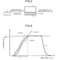
- FIG. 4 is a diagram for explaining the relationship between the reference waveform and the initial gradient that are incorporated in the judgment as to whether the optical axis is suitably adjusted in the optical source manufacturing apparatus according to the present embodiment.
- the graph shown in FIG. 4 shows a reference waveform V 1 produced when the device is driven under pulse width control (duty control with 30% duty ratio).
- the reference waveform is a current waveform in proportion to the amount of laser light detected by the light receiving device 6 during a period of time from the start to the end of the current supplied to the laser device 2 for one pulse, and corresponds to ON/OFF of the pulse.
- the current rises from zero at an initial gradient Av, and flows at the maximum current Iv for a certain period of time, and then falls back to zero.
- the minimum value Iwmin of the maximum current value Iw of the drive waveform I, and the maximum value Awmax and the minimum value Awmin of the inclination of the rising edge, or in other words the initial gradient Aw are defined for each reference waveform to determine whether a drive waveform I detected by the light receiving device 6 falls in a reference range of the reference waveform.
- FIG. 5 is a diagram for explaining an example of judgment as to whether the optical axis is suitably adjusted in the light source manufacturing apparatus according to the present embodiment.
- the hatched area of this drawing represents an area of the drive waveform that is judged as being in the reference range.
- the drive waveform in the reference range is indicated by a solid line, whereas the drive waveform outside the reference range is indicated by dashed lines.
- the drive waveform W 4 is also out of the reference range because Iw ⁇ Iwmin.
- the laser device 2 is slightly moved again in any of the six axial directions including the X-axis, Y-axis, and Y-axis directions and ⁇ x, ⁇ y, and ⁇ z directions.
- the moving stage 4 is moved in the Z-axis, ⁇ x, X-axis, and ⁇ y directions, which are axes related to the efficiency of the resonance inside the optical waveguide 1 a .
- the amount of light is measured by the power meter 7 together with the drive waveform, and the optical axis is adjusted such that both the drive waveform and the amount of light (the relative positions of the laser device 2 and the SHG device 1 ) would be satisfied.
- the light source manufacturing apparatus 100 applies a suitable amount of adhesive or the like to the connecting portion of the laser device 2 and the SHG device 1 by use of the dispenser 10 or the like.
- the laser device 2 and the SHG device 1 are thereby firmly attached to each other.
- the dispenser 10 and the fixed stage 3 are both arranged above a position switching mechanism (not shown).
- the fixed stage 3 moves to a position above the laser device 2 to perform the optical axis adjusting process.
- the dispenser 10 moves to a position above the laser device 2 to perform the adhering and fixing process.
- an adhesive or the like is applied to the connecting portion of the laser device 2 and the SHG device 1 by use of the dispenser 10 or the like, without re-adjusting the optical axis, and the laser device 2 and the SHG device 1 are firmly attached to each other.
- the laser light is emitted from the SHG device 1 (optical axis direction) in a vertical direction when the optical direction is adjusted.
- the direction of the laser light emitted from the SHG device 1 may not be vertical (for example, it may be horizontal).
- the optical axis is adjusted by placing the laser device 2 onto the moving stage 4 , but the optical axis may be adjusted by moving the SHG device 1 . Even in such a configuration, the rest of the structure and the operation is the same as in the light source manufacturing apparatus 100 illustrated in FIG. 1 , and the same effects can be obtained.
- the optical axis may be judged as being sufficiently adjusted, if the drive waveform produced after the adjustment of the optical axis falls in a predetermined reference range, and therefore the adjustment of the optical axis may be terminated even if the optical axis can be re-adjusted to further increase the amount of light.
- the SHG device 1 is adopted as a wavelength converting device.
- the wavelength converting device is not limited to a device that generates second harmonic waves, but may be a device that generates third or fourth harmonic waves.
- a green light source or a blue light source can be obtained with reduced fluctuations in the responsiveness of the laser light.
- the optical axis is adjusted to have the power meter 7 detect the amount of light greater than or equal to the predetermined value, readjustment of the optical axis is conducted based on the drive waveform.
- the adjustment of the optical axis can be achieved in a short period of time.
- a light source device is manufactured by adjusting the optical axes of the laser device and the wavelength converting device to bring the drive waveform of the laser light into a predetermined reference range.
- a light source device that maintains the responsiveness of the laser light at a certain level can be manufactured.
Landscapes
- Physics & Mathematics (AREA)
- Electromagnetism (AREA)
- Engineering & Computer Science (AREA)
- Plasma & Fusion (AREA)
- Optics & Photonics (AREA)
- Optical Modulation, Optical Deflection, Nonlinear Optics, Optical Demodulation, Optical Logic Elements (AREA)
- Optical Couplings Of Light Guides (AREA)
Abstract
Description
Claims (4)
Applications Claiming Priority (2)
| Application Number | Priority Date | Filing Date | Title |
|---|---|---|---|
| JP2009268774A JP4964289B2 (en) | 2009-11-26 | 2009-11-26 | Light source device manufacturing apparatus and light source device manufacturing method |
| JP2009-268774 | 2009-11-26 |
Publications (2)
| Publication Number | Publication Date |
|---|---|
| US20110119899A1 US20110119899A1 (en) | 2011-05-26 |
| US8314378B2 true US8314378B2 (en) | 2012-11-20 |
Family
ID=44060977
Family Applications (1)
| Application Number | Title | Priority Date | Filing Date |
|---|---|---|---|
| US12/782,745 Expired - Fee Related US8314378B2 (en) | 2009-11-26 | 2010-05-19 | Apparatus and method for manufacturing light source device |
Country Status (2)
| Country | Link |
|---|---|
| US (1) | US8314378B2 (en) |
| JP (1) | JP4964289B2 (en) |
Citations (4)
| Publication number | Priority date | Publication date | Assignee | Title |
|---|---|---|---|---|
| JPH01180507A (en) | 1988-01-13 | 1989-07-18 | Nec Corp | Method for adjusting optical axis |
| JP2003046184A (en) | 2001-08-01 | 2003-02-14 | Fuji Photo Film Co Ltd | Device and method for assembling optical product |
| JP2003172856A (en) | 2001-12-06 | 2003-06-20 | Fuji Photo Film Co Ltd | Method and device for assembling optical product |
| JP2004109256A (en) | 2002-09-13 | 2004-04-08 | Matsushita Electric Ind Co Ltd | Optical element adjusting method and apparatus, optical device manufacturing method and optical unit using the method |
-
2009
- 2009-11-26 JP JP2009268774A patent/JP4964289B2/en not_active Expired - Fee Related
-
2010
- 2010-05-19 US US12/782,745 patent/US8314378B2/en not_active Expired - Fee Related
Patent Citations (4)
| Publication number | Priority date | Publication date | Assignee | Title |
|---|---|---|---|---|
| JPH01180507A (en) | 1988-01-13 | 1989-07-18 | Nec Corp | Method for adjusting optical axis |
| JP2003046184A (en) | 2001-08-01 | 2003-02-14 | Fuji Photo Film Co Ltd | Device and method for assembling optical product |
| JP2003172856A (en) | 2001-12-06 | 2003-06-20 | Fuji Photo Film Co Ltd | Method and device for assembling optical product |
| JP2004109256A (en) | 2002-09-13 | 2004-04-08 | Matsushita Electric Ind Co Ltd | Optical element adjusting method and apparatus, optical device manufacturing method and optical unit using the method |
Non-Patent Citations (1)
| Title |
|---|
| Office Action (Decision of a Patent Grant) dated Feb. 28, 2012, issued in the corresponding Japanese Patent Application No. 2009-268774, and an English Translation thereof. (3 pages). |
Also Published As
| Publication number | Publication date |
|---|---|
| JP4964289B2 (en) | 2012-06-27 |
| JP2011112843A (en) | 2011-06-09 |
| US20110119899A1 (en) | 2011-05-26 |
Similar Documents
| Publication | Publication Date | Title |
|---|---|---|
| US7941051B2 (en) | Laser optical device and control method of actuator | |
| CN109073844B (en) | Optical alignment of optical subassemblies with optoelectronic devices | |
| US6688783B2 (en) | Method of fabricating an optical module including a lens attached to a platform of the optical module | |
| US20100272134A1 (en) | Rapid Alignment Methods For Optical Packages | |
| JP2014138021A (en) | Alignment device and alignment method using the same | |
| KR101258167B1 (en) | Method and apparatus for driving semiconductor lasers, and method and apparatus for deriving drive current patterns for semiconductor lasers | |
| US10379300B2 (en) | Method for assembling optical module | |
| CN111050978B (en) | Laser device | |
| US8314378B2 (en) | Apparatus and method for manufacturing light source device | |
| JPH0266504A (en) | Optical transmitter module manufacturing equipment | |
| WO2019221034A1 (en) | Laser device and laser processing device using same | |
| KR101226807B1 (en) | Stage Device for transfering a Specimen and Drive Method of the Same | |
| JP4484835B2 (en) | Beam irradiation device | |
| WO2018128118A1 (en) | Optical communication device | |
| CN117805974A (en) | Automatic coupling method for optical fibers | |
| JP6920035B2 (en) | Alignment method and alignment device | |
| JP6743393B2 (en) | Displacement measuring device | |
| JP5039117B2 (en) | Light source manufacturing apparatus and light source manufacturing method | |
| JP2004071591A (en) | Semiconductor laser light source device | |
| JP5043918B2 (en) | Light source manufacturing method and light source manufacturing apparatus | |
| JP2021189130A (en) | Waveguide characteristic measuring device and waveguide characteristic measuring method | |
| US20070280084A1 (en) | Optical pickup | |
| Yokoyama et al. | New passive alignment method of channel waveguide device using height control spacers | |
| Feldman et al. | Highly efficient and reliable 1 kW QCW laser stacks with diffraction limited fast axis beam collimation | |
| CN118936854A (en) | An optical inspection system that accurately matches the optimal conversion efficiency of laser crystals |
Legal Events
| Date | Code | Title | Description |
|---|---|---|---|
| AS | Assignment |
Owner name: MITSUBISHI ELECTRIC CORPORATION, JAPAN Free format text: ASSIGNMENT OF ASSIGNORS INTEREST;ASSIGNORS:OE, SHINICHI;IKEDA, KAZUTAKA;NAKAMURA, AKIRA;AND OTHERS;REEL/FRAME:024406/0317 Effective date: 20100427 |
|
| ZAAA | Notice of allowance and fees due |
Free format text: ORIGINAL CODE: NOA |
|
| ZAAB | Notice of allowance mailed |
Free format text: ORIGINAL CODE: MN/=. |
|
| STCF | Information on status: patent grant |
Free format text: PATENTED CASE |
|
| FEPP | Fee payment procedure |
Free format text: PAYOR NUMBER ASSIGNED (ORIGINAL EVENT CODE: ASPN); ENTITY STATUS OF PATENT OWNER: LARGE ENTITY |
|
| FPAY | Fee payment |
Year of fee payment: 4 |
|
| MAFP | Maintenance fee payment |
Free format text: PAYMENT OF MAINTENANCE FEE, 8TH YEAR, LARGE ENTITY (ORIGINAL EVENT CODE: M1552); ENTITY STATUS OF PATENT OWNER: LARGE ENTITY Year of fee payment: 8 |
|
| LAPS | Lapse for failure to pay maintenance fees |
Free format text: PATENT EXPIRED FOR FAILURE TO PAY MAINTENANCE FEES (ORIGINAL EVENT CODE: EXP.); ENTITY STATUS OF PATENT OWNER: LARGE ENTITY |
|
| STCH | Information on status: patent discontinuation |
Free format text: PATENT EXPIRED DUE TO NONPAYMENT OF MAINTENANCE FEES UNDER 37 CFR 1.362 |
|
| FP | Lapsed due to failure to pay maintenance fee |
Effective date: 20241120 |