US8309977B2 - Organic light-emitting diode module - Google Patents
Organic light-emitting diode module Download PDFInfo
- Publication number
- US8309977B2 US8309977B2 US13/052,112 US201113052112A US8309977B2 US 8309977 B2 US8309977 B2 US 8309977B2 US 201113052112 A US201113052112 A US 201113052112A US 8309977 B2 US8309977 B2 US 8309977B2
- Authority
- US
- United States
- Prior art keywords
- organic light
- conductive elements
- substrate
- conductive
- bus line
- Prior art date
- Legal status (The legal status is an assumption and is not a legal conclusion. Google has not performed a legal analysis and makes no representation as to the accuracy of the status listed.)
- Active, expires
Links
Images


Classifications
-
- H—ELECTRICITY
- H10—SEMICONDUCTOR DEVICES; ELECTRIC SOLID-STATE DEVICES NOT OTHERWISE PROVIDED FOR
- H10K—ORGANIC ELECTRIC SOLID-STATE DEVICES
- H10K50/00—Organic light-emitting devices
- H10K50/80—Constructional details
- H10K50/805—Electrodes
-
- H—ELECTRICITY
- H10—SEMICONDUCTOR DEVICES; ELECTRIC SOLID-STATE DEVICES NOT OTHERWISE PROVIDED FOR
- H10K—ORGANIC ELECTRIC SOLID-STATE DEVICES
- H10K50/00—Organic light-emitting devices
- H10K50/80—Constructional details
- H10K50/88—Terminals, e.g. bond pads
-
- H—ELECTRICITY
- H10—SEMICONDUCTOR DEVICES; ELECTRIC SOLID-STATE DEVICES NOT OTHERWISE PROVIDED FOR
- H10K—ORGANIC ELECTRIC SOLID-STATE DEVICES
- H10K59/00—Integrated devices, or assemblies of multiple devices, comprising at least one organic light-emitting element covered by group H10K50/00
- H10K59/10—OLED displays
- H10K59/18—Tiled displays
Definitions
- the invention generally relates to a light-emitting module, and more particularly relates to an organic light-emitting diode (OLED) module.
- OLED organic light-emitting diode
- An organic electroluminescence display is a self-emissive display.
- the organic electroluminescence display has the advantages of no viewing angle restriction, low production costs, high response speed (at least one hundred times the response speed of a liquid crystal display), low power consumption, a direct current driving function applicable to a portable device, a wide operating temperature range, light weight, and the ability to be miniaturized together with the hardware. Therefore, the organic electroluminescence device has great potential for development, and is expected to be the new flat panel display in the next generation.
- the organic electroluminescence display is composed of two bus lines and an organic light-emitting layer configured between the two bus lines.
- the lower bus line is made of a transparent conductive material, such that light generated by the organic light-emitting layer can be transmitted out of the lower bus line.
- the greater the distance from the organic light-emitting layer to an external electrode the greater the voltage drop-out caused by resistance. This is because the long conductive wire connected between the external electrode and the organic light-emitting layer leads to an increase in the resistance. As such, the less the voltage across the organic light-emitting layer, the lower the luminance.
- the conventional solution to the aforesaid issue often refers to expansion of the cross-section area of the bus line for increasing the amount of power transmission.
- the contact positions between a flexible circuit board and a substrate can be increased, so as to increase the number of contacts for signal input.
- the former solution may result in expansion of the substrate or reduction of the aperture ratio, while the latter solution may increase the volume of the flexible circuit board and the wire bonding costs. Consequently, the above-mentioned issue cannot be efficiently resolved.
- the invention is directed to an OLED module that has constant voltage supply and thus can ensure uniformity of luminance.
- the invention provides an OLED module that includes a substrate, at least one conductive wire, a bus line, an organic light-emitting device layer, and a plurality of conductive elements.
- the bus line, the organic light-emitting device layer, and the conductive elements are configured on the substrate.
- the organic light-emitting device layer and the conductive elements are electrically connected to the bus line, respectively.
- the conductive wire is configured next to the conductive elements and electrically connected to the conductive elements.
- connection portion between each of the conductive elements and the bus line has a rough surface.
- the OLED module further includes a conductive adhesion layer that is configured between each of the conductive elements and the bus line.
- the conductive elements are located at the peripheries of the substrate.
- the organic light-emitting device layer includes a plurality of OLED units arranged in arrays.
- the conductive wire is connected to the conductive elements between any two of the OLED units through the substrate.
- the conductive elements are conductive bumps or conductive protrusions substantially configured on the substrate.
- each of the conductive elements is an elastic element substantially configured on the substrate and made of a conductive material.
- a voltage drop-out of each of the conductive elements relative to the substrate is less than 10 ⁇ after each of the conductive elements is electrically conducted.
- the OLED module provides the voltage source required by the organic light-emitting device layer through the conductive elements of the OLED module and the conductive wire that is electrically connected to the conductive elements.
- the voltage can be constantly applied to each region of the organic light-emitting device layer.
- the conventional issue of the voltage drop-out caused by the different locations of the bus line can be resolved, and different luminance efficacy of the organic light-emitting device layer caused by different voltages applied to the organic light-emitting device layer can be precluded.
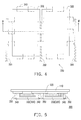
- FIG. 1 is a top view illustrating an OLED module according to an embodiment of the invention.
- FIG. 2 is a cross-sectional view illustrating the OLED module depicted in FIG. 1 taken along a line A-A′.
- FIG. 3 is a cross-sectional view illustrating an OLED module according to another embodiment of the invention.
- FIG. 4 is a top view illustrating an OLED module according to yet another embodiment of the invention.
- FIG. 5 is a cross-sectional view illustrating the OLED module depicted in FIG. 4 taken along a line B-B′.
- FIG. 1 is a top view illustrating an OLED module according to an embodiment of the invention.
- FIG. 2 is a cross-sectional view illustrating the OLED module depicted in FIG. 1 taken along a line A-A′.
- the OLED module 100 includes a substrate 110 , a bus line 120 , an organic light-emitting device layer 130 , a plurality of conductive elements 140 , conductive wires 150 configured next to the conductive elements 140 and electrically connected to the conductive elements 140 , and a frame 160 accommodating the above-mentioned components.
- the bus line 120 , the organic light-emitting device layer 130 , and the conductive elements 140 are configured on the substrate 110 .
- the organic light-emitting device layer 130 and the conductive elements 140 are electrically connected to the bus line 120 , respectively.
- only two conductive wires 150 are depicted, which should however not be construed as a limitation to this invention.
- the OLED module 100 of this embodiment provides the voltage source required by the organic light-emitting device layer 130 through the conductive elements 140 configured on the substrate 110 , such that voltages applied to each region of the organic light-emitting device layer 130 are almost the same, and that the luminance of each region of the organic light-emitting device layer 130 can be uniformized.
- the substrate 110 is a transparent substrate, such as a transparent glass substrate or a transparent flexible substrate.
- the substrate 110 is mainly used to carry components of an organic electroluminescence device.
- the substrate 110 is made of a transparent material or a light-transmissive material.
- the organic electroluminescence device generating the light that is emitted from the substrate 110 is also referred to as a bottom emission organic electroluminescence device.
- the organic light-emitting device layer 130 is located on the substrate 110 .
- the organic light-emitting device layer 130 includes a first electrode layer 132 , a light-emitting layer 134 , and a second electrode layer 136 .
- the first electrode layer 132 is configured on the substrate 110
- the light-emitting layer 134 is configured on the first electrode layer 132
- the second electrode layer 136 is configured on the light-emitting layer 134 .
- the first electrode layer 132 is a transparent electrode layer and can be made of metal oxide, such as indium tin oxide (ITO), indium zinc oxide (IZO), and so forth.
- the light-emitting layer 134 is an organic light-emitting layer that can include a red organic light-emitting pattern, a green organic light-emitting pattern, a blue organic light-emitting pattern, or a light-emitting pattern of other colors generated by mixing light of various spectra (i.e., white, orange, purple, and so on).
- the second electrode layer 136 can be a metal electrode layer.
- the organic light-emitting device layer 130 can further include an electron injection layer, a hole injection layer, an electron transporting layer, a hole transporting layer, and so on.
- the conductive elements 140 of this embodiment are conductive bumps or conductive protrusions substantially configured at the peripheries of the substrate 110 .
- the conductive elements 140 directly press the bus line 120 ; namely, the conductive elements 140 exert a pressing force on the bus line 120 , and the pressing force is preferably greater than 50 g/cm 2 .
- a connection portion between each of the conductive elements 140 and the bus line 120 has a rough surface S 1 for increasing partial pressure on the conductive elements 140 and the substrate 110 .
- an embossment process can be performed on the surface of the conductive elements 140 to form the rough surface S 1 , while other processes for forming the rough surface S 1 are also applicable in the invention.
- the OLED module 100 of this embodiment further includes a conductive adhesion layer 170 which is formed by coating the space between the conductive elements 140 and the bus line 120 with the conducive adhesive, so as to enhance electrical connection between the conductive elements 140 and the bus line 120 .
- a conductive adhesion layer 170 which is formed by coating the space between the conductive elements 140 and the bus line 120 with the conducive adhesive, so as to enhance electrical connection between the conductive elements 140 and the bus line 120 .
- any method for enhancing the electrical connection between the conductive elements 140 and the bus line 120 is applicable in this embodiment.
- a voltage drop-out of each of the conductive elements 140 relative to the substrate 110 must be less than 10 ⁇ , such that the electric current passing the conducive elements 140 tends to be equalized.
- the voltages applied on each region of the organic light-emitting device layer 130 are almost the same, and the OLED module 100 can have constant luminance efficacy.
- FIG. 3 is a cross-sectional view illustrating an OLED module according to another embodiment of the invention.
- each of the conductive elements 240 of this embodiment is an elastic element substantially configured on the substrate 110 and made of a conductive material.
- the conductive elements 240 can be electrically connected to the bus line 120 because the substrate 110 is clipped by the conductive elements 240 . That is to say, in this embodiment, conductive clamping apparatuses configured on the substrate 110 can also serve as the conductive elements 240 in the OLED module 200 , and the bus line 120 is electrically connected to the conductive elements 240 , so as to supply the voltage source required by the organic light-emitting device layer 130 .
- the conductive bumps, the conductive protrusions, or any elastic conductive element configured on the substrate 110 can be electrically connected to the bus line 120 , so as to supply the voltage source required by the organic light-emitting device layer 130 and further equalize the voltages that are applied to each region of the organic light-emitting device layer 130 .
- FIG. 4 is a top view illustrating an OLED module according to yet another embodiment of the invention.
- FIG. 5 is a cross-sectional view illustrating the OLED module depicted in FIG. 4 taken along a line B-B′.
- the organic light-emitting layer 330 includes a plurality of OLED units 332 arranged in arrays, and only two of the OLED units 332 are depicted herein.
- the conductive wires 350 connect the conductive elements 340 (herein referred to as the conductive bumps or the conductive protrusions, for instance) between any two of the OLED units 332 through the substrate 110 .
- the OLED module 300 can supply the OLED units 332 with power through the conductive elements 340 on the substrate 110 , and thereby the conventional negative impact on the voltages applied to the OLED units 332 , which is caused by different locations of the bus line 120 , can be prevented.
- the OLED module described in the previous embodiments of the invention can stabilize the voltages applied to the organic light-emitting layer by means of the conductive elements configured on the substrate.
- the conductive elements can be the conductive bumps, the conductive protrusions, or the elastic conductive clamping apparatuses configured on the substrate.
- the existing components of the OLED module are sufficient to achieve constant and stable voltage supply.
- the voltage constantly and stably applied on each region of the OLED module can guarantee the uniform luminance efficacy of the OLED module.
Landscapes
- Physics & Mathematics (AREA)
- Optics & Photonics (AREA)
- Electroluminescent Light Sources (AREA)
Abstract
Description
Claims (8)
Applications Claiming Priority (3)
| Application Number | Priority Date | Filing Date | Title |
|---|---|---|---|
| TW99134601 | 2010-10-11 | ||
| TW99134601A | 2010-10-11 | ||
| TW099134601A TWI434598B (en) | 2010-10-11 | 2010-10-11 | Organic light emitting diode module |
Publications (2)
| Publication Number | Publication Date |
|---|---|
| US20120086025A1 US20120086025A1 (en) | 2012-04-12 |
| US8309977B2 true US8309977B2 (en) | 2012-11-13 |
Family
ID=45924440
Family Applications (1)
| Application Number | Title | Priority Date | Filing Date |
|---|---|---|---|
| US13/052,112 Active 2031-03-23 US8309977B2 (en) | 2010-10-11 | 2011-03-21 | Organic light-emitting diode module |
Country Status (2)
| Country | Link |
|---|---|
| US (1) | US8309977B2 (en) |
| TW (1) | TWI434598B (en) |
Families Citing this family (4)
| Publication number | Priority date | Publication date | Assignee | Title |
|---|---|---|---|---|
| JP2014154213A (en) * | 2013-02-04 | 2014-08-25 | Toshiba Corp | Organic electroluminescent element, illumination device and illumination system |
| JP6483926B2 (en) * | 2016-05-23 | 2019-03-13 | 堺ディスプレイプロダクト株式会社 | Display device |
| CN106229422B (en) | 2016-09-05 | 2019-05-10 | 京东方科技集团股份有限公司 | Lighting components and lighting fixtures |
| TWI778282B (en) * | 2019-07-22 | 2022-09-21 | 機光科技股份有限公司 | Multi-chip organic light emitting diode flexible lamp module structure |
Citations (1)
| Publication number | Priority date | Publication date | Assignee | Title |
|---|---|---|---|---|
| US6995035B2 (en) * | 2003-06-16 | 2006-02-07 | Eastman Kodak Company | Method of making a top-emitting OLED device having improved power distribution |
-
2010
- 2010-10-11 TW TW099134601A patent/TWI434598B/en active
-
2011
- 2011-03-21 US US13/052,112 patent/US8309977B2/en active Active
Patent Citations (1)
| Publication number | Priority date | Publication date | Assignee | Title |
|---|---|---|---|---|
| US6995035B2 (en) * | 2003-06-16 | 2006-02-07 | Eastman Kodak Company | Method of making a top-emitting OLED device having improved power distribution |
Also Published As
| Publication number | Publication date |
|---|---|
| TW201216760A (en) | 2012-04-16 |
| TWI434598B (en) | 2014-04-11 |
| US20120086025A1 (en) | 2012-04-12 |
Similar Documents
| Publication | Publication Date | Title |
|---|---|---|
| US7909480B2 (en) | Light source module, method of fabricating the same, and display device having the light source module | |
| JP5796171B2 (en) | Light emitting module | |
| US20130015772A1 (en) | Lighting device | |
| CN104253149A (en) | OLED (Organic Light Emitting Diode) display | |
| US20120112237A1 (en) | Led package structure | |
| KR102931287B1 (en) | Display apparatus and light apparatus thereof | |
| CN113517327A (en) | Display panel, display device and display method | |
| US8309977B2 (en) | Organic light-emitting diode module | |
| US12321063B2 (en) | Display apparatus and light source device thereof | |
| TWI556484B (en) | Organic light emitting diode module | |
| US9166187B2 (en) | Organic light emitting device and power supply device thereof | |
| US20180102097A1 (en) | Display device | |
| US9013096B2 (en) | Light emitting module | |
| US20080211992A1 (en) | Diode substrate of LCD | |
| US6798137B2 (en) | Apparatus and method for warpage compensation of a display panel substrate assembly | |
| JP2012018895A (en) | Organic el lighting device | |
| US12085808B2 (en) | Display apparatus | |
| US20230307587A1 (en) | Display apparatus | |
| CN102054855B (en) | Organic Light Emitting Diode Module | |
| CN107610604B (en) | LED chip, array substrate, display panel and display device | |
| US12085802B2 (en) | Display apparatus and light source apparatus thereof | |
| US12032241B2 (en) | Display apparatus and light source apparatus including an optical member | |
| CN105720023B (en) | Display and its thermoelectric conduction element | |
| EP4050408B1 (en) | Display device and light source device thereof | |
| CN208572516U (en) | display device |
Legal Events
| Date | Code | Title | Description |
|---|---|---|---|
| AS | Assignment |
Owner name: AU OPTRONICS CORPORATION, TAIWAN Free format text: ASSIGNMENT OF ASSIGNORS INTEREST;ASSIGNOR:MO, YAO-AN;REEL/FRAME:026001/0417 Effective date: 20101124 |
|
| STCF | Information on status: patent grant |
Free format text: PATENTED CASE |
|
| FPAY | Fee payment |
Year of fee payment: 4 |
|
| MAFP | Maintenance fee payment |
Free format text: PAYMENT OF MAINTENANCE FEE, 8TH YEAR, LARGE ENTITY (ORIGINAL EVENT CODE: M1552); ENTITY STATUS OF PATENT OWNER: LARGE ENTITY Year of fee payment: 8 |
|
| MAFP | Maintenance fee payment |
Free format text: PAYMENT OF MAINTENANCE FEE, 12TH YEAR, LARGE ENTITY (ORIGINAL EVENT CODE: M1553); ENTITY STATUS OF PATENT OWNER: LARGE ENTITY Year of fee payment: 12 |
|
| AS | Assignment |
Owner name: NEOLAYER LLC, TEXAS Free format text: ASSIGNMENT OF ASSIGNORS INTEREST;ASSIGNOR:AUO CORPORATION;REEL/FRAME:072266/0941 Effective date: 20250701 |