US8309442B2 - Semiconductor stacking layer and fabricating method thereof - Google Patents
Semiconductor stacking layer and fabricating method thereof Download PDFInfo
- Publication number
- US8309442B2 US8309442B2 US13/506,305 US201213506305A US8309442B2 US 8309442 B2 US8309442 B2 US 8309442B2 US 201213506305 A US201213506305 A US 201213506305A US 8309442 B2 US8309442 B2 US 8309442B2
- Authority
- US
- United States
- Prior art keywords
- layer
- doped
- fabricating method
- silicon layer
- cross
- Prior art date
- Legal status (The legal status is an assumption and is not a legal conclusion. Google has not performed a legal analysis and makes no representation as to the accuracy of the status listed.)
- Active
Links
- 239000004065 semiconductor Substances 0.000 title claims abstract description 31
- 238000000034 method Methods 0.000 title claims abstract description 23
- 229910021424 microcrystalline silicon Inorganic materials 0.000 claims abstract description 59
- 230000007547 defect Effects 0.000 claims abstract description 34
- 238000004381 surface treatment Methods 0.000 claims abstract description 30
- 239000000758 substrate Substances 0.000 claims abstract description 12
- 229910021417 amorphous silicon Inorganic materials 0.000 claims abstract description 10
- XKRFYHLGVUSROY-UHFFFAOYSA-N Argon Chemical compound [Ar] XKRFYHLGVUSROY-UHFFFAOYSA-N 0.000 claims description 8
- IJGRMHOSHXDMSA-UHFFFAOYSA-N Atomic nitrogen Chemical compound N#N IJGRMHOSHXDMSA-UHFFFAOYSA-N 0.000 claims description 8
- 229910052786 argon Inorganic materials 0.000 claims description 4
- 229910052757 nitrogen Inorganic materials 0.000 claims description 4
- 239000001257 hydrogen Substances 0.000 claims description 3
- 229910052739 hydrogen Inorganic materials 0.000 claims description 3
- UFHFLCQGNIYNRP-UHFFFAOYSA-N Hydrogen Chemical compound [H][H] UFHFLCQGNIYNRP-UHFFFAOYSA-N 0.000 claims description 2
- 238000004519 manufacturing process Methods 0.000 abstract description 8
- 230000015572 biosynthetic process Effects 0.000 description 6
- 238000009413 insulation Methods 0.000 description 6
- 239000000463 material Substances 0.000 description 6
- 239000010409 thin film Substances 0.000 description 5
- 230000008901 benefit Effects 0.000 description 4
- XUIMIQQOPSSXEZ-UHFFFAOYSA-N Silicon Chemical group [Si] XUIMIQQOPSSXEZ-UHFFFAOYSA-N 0.000 description 2
- 230000002349 favourable effect Effects 0.000 description 2
- 239000004973 liquid crystal related substance Substances 0.000 description 2
- 239000007769 metal material Substances 0.000 description 2
- 230000002411 adverse Effects 0.000 description 1
- 239000007795 chemical reaction product Substances 0.000 description 1
- 230000003247 decreasing effect Effects 0.000 description 1
- 125000004435 hydrogen atom Chemical class [H]* 0.000 description 1
- 238000012986 modification Methods 0.000 description 1
- 230000004048 modification Effects 0.000 description 1
- 230000005693 optoelectronics Effects 0.000 description 1
- 229910052710 silicon Inorganic materials 0.000 description 1
Images


Classifications
-
- H—ELECTRICITY
- H01—ELECTRIC ELEMENTS
- H01L—SEMICONDUCTOR DEVICES NOT COVERED BY CLASS H10
- H01L21/00—Processes or apparatus adapted for the manufacture or treatment of semiconductor or solid state devices or of parts thereof
- H01L21/02—Manufacture or treatment of semiconductor devices or of parts thereof
- H01L21/02104—Forming layers
- H01L21/02365—Forming inorganic semiconducting materials on a substrate
- H01L21/02518—Deposited layers
- H01L21/02521—Materials
- H01L21/02524—Group 14 semiconducting materials
- H01L21/02532—Silicon, silicon germanium, germanium
-
- H—ELECTRICITY
- H01—ELECTRIC ELEMENTS
- H01L—SEMICONDUCTOR DEVICES NOT COVERED BY CLASS H10
- H01L21/00—Processes or apparatus adapted for the manufacture or treatment of semiconductor or solid state devices or of parts thereof
- H01L21/02—Manufacture or treatment of semiconductor devices or of parts thereof
- H01L21/02104—Forming layers
- H01L21/02365—Forming inorganic semiconducting materials on a substrate
- H01L21/02436—Intermediate layers between substrates and deposited layers
- H01L21/02439—Materials
- H01L21/02441—Group 14 semiconducting materials
- H01L21/0245—Silicon, silicon germanium, germanium
-
- H—ELECTRICITY
- H01—ELECTRIC ELEMENTS
- H01L—SEMICONDUCTOR DEVICES NOT COVERED BY CLASS H10
- H01L21/00—Processes or apparatus adapted for the manufacture or treatment of semiconductor or solid state devices or of parts thereof
- H01L21/02—Manufacture or treatment of semiconductor devices or of parts thereof
- H01L21/02104—Forming layers
- H01L21/02365—Forming inorganic semiconducting materials on a substrate
- H01L21/02436—Intermediate layers between substrates and deposited layers
- H01L21/02494—Structure
- H01L21/02513—Microstructure
-
- H—ELECTRICITY
- H01—ELECTRIC ELEMENTS
- H01L—SEMICONDUCTOR DEVICES NOT COVERED BY CLASS H10
- H01L21/00—Processes or apparatus adapted for the manufacture or treatment of semiconductor or solid state devices or of parts thereof
- H01L21/02—Manufacture or treatment of semiconductor devices or of parts thereof
- H01L21/02104—Forming layers
- H01L21/02365—Forming inorganic semiconducting materials on a substrate
- H01L21/02518—Deposited layers
- H01L21/02587—Structure
- H01L21/0259—Microstructure
- H01L21/02595—Microstructure polycrystalline
-
- H—ELECTRICITY
- H01—ELECTRIC ELEMENTS
- H01L—SEMICONDUCTOR DEVICES NOT COVERED BY CLASS H10
- H01L21/00—Processes or apparatus adapted for the manufacture or treatment of semiconductor or solid state devices or of parts thereof
- H01L21/02—Manufacture or treatment of semiconductor devices or of parts thereof
- H01L21/02104—Forming layers
- H01L21/02365—Forming inorganic semiconducting materials on a substrate
- H01L21/02656—Special treatments
- H01L21/02658—Pretreatments
-
- H—ELECTRICITY
- H01—ELECTRIC ELEMENTS
- H01L—SEMICONDUCTOR DEVICES NOT COVERED BY CLASS H10
- H01L29/00—Semiconductor devices adapted for rectifying, amplifying, oscillating or switching, or capacitors or resistors with at least one potential-jump barrier or surface barrier, e.g. PN junction depletion layer or carrier concentration layer; Details of semiconductor bodies or of electrodes thereof ; Multistep manufacturing processes therefor
- H01L29/66—Types of semiconductor device ; Multistep manufacturing processes therefor
- H01L29/66007—Multistep manufacturing processes
- H01L29/66075—Multistep manufacturing processes of devices having semiconductor bodies comprising group 14 or group 13/15 materials
- H01L29/66227—Multistep manufacturing processes of devices having semiconductor bodies comprising group 14 or group 13/15 materials the devices being controllable only by the electric current supplied or the electric potential applied, to an electrode which does not carry the current to be rectified, amplified or switched, e.g. three-terminal devices
- H01L29/66409—Unipolar field-effect transistors
- H01L29/66477—Unipolar field-effect transistors with an insulated gate, i.e. MISFET
- H01L29/66742—Thin film unipolar transistors
- H01L29/6675—Amorphous silicon or polysilicon transistors
- H01L29/66765—Lateral single gate single channel transistors with inverted structure, i.e. the channel layer is formed after the gate
-
- H—ELECTRICITY
- H01—ELECTRIC ELEMENTS
- H01L—SEMICONDUCTOR DEVICES NOT COVERED BY CLASS H10
- H01L29/00—Semiconductor devices adapted for rectifying, amplifying, oscillating or switching, or capacitors or resistors with at least one potential-jump barrier or surface barrier, e.g. PN junction depletion layer or carrier concentration layer; Details of semiconductor bodies or of electrodes thereof ; Multistep manufacturing processes therefor
- H01L29/66—Types of semiconductor device ; Multistep manufacturing processes therefor
- H01L29/68—Types of semiconductor device ; Multistep manufacturing processes therefor controllable by only the electric current supplied, or only the electric potential applied, to an electrode which does not carry the current to be rectified, amplified or switched
- H01L29/76—Unipolar devices, e.g. field effect transistors
- H01L29/772—Field effect transistors
- H01L29/78—Field effect transistors with field effect produced by an insulated gate
- H01L29/786—Thin film transistors, i.e. transistors with a channel being at least partly a thin film
- H01L29/78606—Thin film transistors, i.e. transistors with a channel being at least partly a thin film with supplementary region or layer in the thin film or in the insulated bulk substrate supporting it for controlling or increasing the safety of the device
- H01L29/78618—Thin film transistors, i.e. transistors with a channel being at least partly a thin film with supplementary region or layer in the thin film or in the insulated bulk substrate supporting it for controlling or increasing the safety of the device characterised by the drain or the source properties, e.g. the doping structure, the composition, the sectional shape or the contact structure
Definitions
- the present application relates to a semiconductor stacking layer and a fabricating method thereof. More particularly, the present application relates to a semiconductor stacking layer composed of an amorphous silicon ( ⁇ -Si) layer and a microcrystalline silicon ( ⁇ c-Si) layer and a fabricating method of the semiconductor stacking layer.
- ⁇ -Si amorphous silicon
- ⁇ c-Si microcrystalline silicon
- TFT-LCDs thin film transistor liquid crystal displays
- a conventional TFT includes a substrate, a gate, a gate insulation layer, a semiconductor layer, an ohmic contact layer, a source, and a drain.
- the gate is disposed on the substrate, and the gate insulation layer is disposed on the substrate and covers the gate.
- the semiconductor layer is disposed on the gate insulation layer and located above the gate.
- the ohmic contact layer is disposed on a portion of the semiconductor layer, and the source and the drain are disposed on the ohmic contact layer.
- the semiconductor layer in the TFT is mainly composed of a channel layer and an ohmic contact layer.
- a material of the channel layer is un-doped ⁇ -Si or lightly doped ⁇ -Si
- a material of the ohmic contact layer is n-type heavily doped ⁇ -Si or n-type heavily doped ⁇ c-Si.
- Compared to the ⁇ -Si material has better doping efficiency and lower resistivity due to the material and structural properties of ⁇ c-Si. Therefore, has been gradually applied to fabrication of the ohmic contact layer.
- the present application is directed to a semiconductor stacking layer having favorable electrical properties.
- the present application is further directed to a fabricating method of a semiconductor stacking layer.
- a fabricating method of a semiconductor stacking layer By applying the method, interface defects existing between an ⁇ -Si layer and a doped ⁇ c-Si layer in the semiconductor stacking layer can be reduced in an effective manner.
- a fabricating method of a semiconductor stacking layer is provided herein.
- the fabricating method is described below.
- Surface treatment is then performed on a surface of the ⁇ -Si layer.
- a doped ⁇ c-Si layer is formed on the treated surface of the ⁇ -Si layer.
- interface defects existing between the ⁇ -Si layer and the doped ⁇ c-Si layer occupy an area in a cross-sectional region having a width of 1.5 micrometers and a thickness of 40 nanometers, and a ratio of the occupied area in the cross-sectional region is equal to or less than 10%.
- the surface treatment includes pretreatment performed on the surface of the ⁇ -Si layer with use of hydrogen plasma, argon plasma, or nitrogen plasma.
- the ratio of the aforesaid occupied area in the cross-sectional region ranges from 2% to 10%.
- the interface defects are inconsecutively distributed on the surface of the ⁇ -Si layer.
- a semiconductor stacking layer including an ⁇ -Si layer and a doped ⁇ c-Si layer is further provided herein.
- the doped ⁇ c-Si layer is located on a surface of the ⁇ -Si layer.
- a plurality of interface defects exist between the ⁇ -Si layer and the doped ⁇ c-Si layer.
- the interface defects occupy an area in a cross-sectional region having a width of 1.5 micrometers and a thickness of 40 nanometers, and a ratio of the occupied area in the cross-sectional region is equal to or less than 10%.
- the ratio of the aforesaid occupied area in the cross-sectional region ranges from 2% to 10%.
- the interface defects are porous.
- the interface defects are inconsecutively distributed between the ⁇ -Si layer and the doped ⁇ c-Si layer.
- the surface treatment is performed on the surface of the ⁇ -Si layer before the doped ⁇ c-Si layer is deposited onto the ⁇ -Si layer, such that the treated surface of the ⁇ -Si layer is conducive to subsequent growth of the doped ⁇ c-Si layer according to the present application.
- the interface defects between the ⁇ -Si layer and the doped ⁇ c-Si layer can be effectively reduced.
- FIGS. 1A to 1C are schematic cross-sectional views illustrating a fabricating method of a semiconductor stacking layer according to an embodiment of the present invention.
- FIG. 2 is a schematic partially enlarged view of FIG. 1C .
- FIGS. 3A to 3D are schematic cross-sectional views illustrating a fabricating method of a TFT according to an embodiment of the present invention.
- FIG. 4 is a schematic partially enlarged view of FIG. 3C .
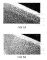
- FIG. 5A is an electron microscope picture showing a doped ⁇ c-Si layer and an ⁇ -Si layer on which surface treatment is not performed
- FIG. 5B is an electron microscope picture showing the doped ⁇ c-Si layer and the ⁇ -Si layer on which the surface treatment is already performed.
- FIGS. 1A to 1C are schematic cross-sectional views illustrating a fabricating method of a semiconductor stacking layer according to an embodiment of the present invention.
- an ⁇ -Si layer 120 is formed on a substrate 110 .
- surface treatment T is performed on a surface 120 a of the ⁇ -Si layer 120 .
- silicon atoms on the surface 120 a of the ⁇ -Si layer 120 can be orderly arranged.
- the treated surface 120 a of the ⁇ -Si layer 120 is conducive to subsequent formation of a doped ⁇ c-Si layer 130 .
- the surface treatment T refers to pretreatment performed on the surface 120 a of the ⁇ -Si layer 120 with use of hydrogen (H 2 ) plasma.
- H 2 plasma improves structural compactness of the surface 120 a of the ⁇ -Si layer 120 so as to enhance bonding strength between the ⁇ -Si layer 120 and the doped ⁇ c-Si layer 130 .
- the surface treatment T can refer to pretreatment performed on the surface 120 a of the ⁇ -Si layer 120 with use of argon plasma or nitrogen plasma.
- the doped ⁇ c-Si layer 130 is formed on the surface 120 a of the ⁇ -Si layer 120 .
- the surface treatment T has already been performed on the surface 120 a of the ⁇ -Si layer 120 .
- the doped ⁇ c-Si layer 130 can be an n-type doped ⁇ c-Si layer, a p-type doped ⁇ c-Si layer, or a combination thereof.
- FIG. 2 is a schematic partially enlarged view of FIG. 1C .
- interface defects D exist between the ⁇ -Si layer 120 and the doped ⁇ c-Si layer 130 .
- the interface defects D occupy an area in a cross-sectional region A having a width of 1.5 micrometers and a thickness of 40 nanometers, and a ratio of the occupied area in the cross-sectional region A is equal to or less than 10%.
- the area occupied by the interface defects D in the cross-sectional region A accounts for 2% ⁇ 10% of the total area of the cross-sectional region A, preferably 5% ⁇ 10%.
- the interface defects D are porous.
- the interface defects D are inconsecutively distributed on the surface 120 a of the ⁇ -Si layer 120 .
- the scopes and types of the applications of the semiconductor stacking layer 100 are not limited herein.
- the semiconductor stacking layer 100 can be further applied to fabrication of other types of semiconductor devices, e.g. TFTs.
- the present invention can also be extensively applied to various end products, e.g. thin film liquid crystal displays or solar cells.
- a fabricating method of the semiconductor stacking layer is described in a second embodiment below when the fabricating method is applied to fabrication of TFTs.
- FIGS. 3A to 3D are schematic cross-sectional views illustrating a fabricating method of a TFT according to an embodiment of the present invention.
- a gate 312 and a gate insulation layer 314 are formed on the substrate 310 .
- the gate 312 is formed by first forming a gate material layer (not shown) on the substrate 310 .
- the gate material layer is patterned to form the gate 312 .
- the gate insulation layer 314 is formed on the gate 312 and the substrate 310 .
- an ⁇ -Si layer 320 is formed on the gate insulation layer 314 , as indicated in FIG. 3A .
- surface treatment T is performed on a surface 320 a of the ⁇ -Si layer 320 .
- silicon atoms on the surface 320 a of the ⁇ -Si layer 320 can be orderly arranged.
- the treated surface 320 a of the ⁇ -Si layer 320 is conducive to subsequent formation of a doped ⁇ c-Si layer 330 .
- interface defects D existing between the ⁇ -Si layer 320 and the doped ⁇ c-Si layer 330 can be effectively reduced.
- the surface treatment T refers to pretreatment performed on the surface 320 a of the ⁇ -Si layer 320 with use of H 2 plasma. Specifically, the pretreatment performed with use of the H 2 plasma improves structural compactness of the surface 320 a of the ⁇ -Si layer 320 so as to enhance bonding strength between the ⁇ -Si layer 320 and the doped ⁇ c-Si layer 330 and to reduce the interface defects.
- the surface treatment T can refer to pretreatment performed on the surface 320 a of the ⁇ -Si layer 320 with use of argon plasma or nitrogen plasma.
- the doped ⁇ c-Si layer 330 is formed on the surface 320 a of the ⁇ -Si layer 320 .
- the surface treatment T has already been performed on the surface 320 a of the ⁇ -Si layer 320 .
- the doped ⁇ c-Si layer 330 can be an n-type doped ⁇ c-Si layer, a p-type doped ⁇ c-Si layer, or a combination thereof.
- a source 350 a and a drain 350 b both covering the doped ⁇ c-Si layer 330 are formed on the substrate 310 in the present embodiment.
- a metal material layer (not shown) is firstly formed on the substrate 310 to cover the doped ⁇ c-Si layer 330 .
- the metal material layer and a portion of the doped ⁇ c-Si layer 330 are then patterned to form a TFT 300 having the source 350 a, the drain 350 b, and the patterned doped ⁇ c-Si layer 330 a, as indicated in FIG. 3D .
- the TFT 300 has favorable electrical properties.
- FIG. 4 is a schematic partially enlarged view of FIG. 3C .
- the interface defects D exist between the ⁇ -Si layer 320 and the doped ⁇ c-Si layer 330 .
- the interface defects D occupy an area in a cross-sectional region A having a width of 1.5 micrometers and a thickness of 40 nanometers, and a ratio of the occupied area in the cross-sectional region A is equal to or less than 10%.
- the area occupied by the interface defects D in the cross-sectional region A accounts for 2% ⁇ 10% of the total area of the cross-sectional region A, preferably 5% ⁇ 10%.
- the interface defects D are porous.
- the interface defects D are inconsecutively distributed on the surface 320 a of the ⁇ -Si layer 320 .
- FIG. 5A is an electron microscope picture showing a doped ⁇ c-Si layer and an ⁇ -Si layer on which surface treatment is not performed
- FIG. 5B is an electron microscope picture showing the doped ⁇ c-Si layer and the ⁇ -Si layer on which the surface treatment is already performed.
- the thickness of the ⁇ -Si layer 120 is approximately 200 ⁇ 220 nanometers
- the thickness of the doped ⁇ c-Si layer 130 is approximately 240 ⁇ 260 nanometers.
- the interface defects D between the ⁇ -Si layer 120 and the doped ⁇ c-Si layer 130 can be effectively reduced.
- the surface treatment is performed on the surface of the ⁇ -Si layer before the doped ⁇ c-Si layer is deposited onto the ⁇ -Si layer, such that the treated surface of the ⁇ -Si layer is conducive to subsequent growth of the doped ⁇ c-Si layer according to the present application.
- the interface defects between the ⁇ -Si layer and the doped ⁇ c-Si layer can be effectively reduced.
Abstract
A fabricating method of a semiconductor stacking layer includes following steps. First, an amorphous silicon (α-Si) layer is formed on a substrate. Surface treatment is then performed on a surface of the α-Si layer. After that, a doped microcrystalline silicon (μc-Si) layer is formed on the treated surface of the α-Si layer, wherein interface defects existing between the α-Si layer and the doped μc-Si layer occupy an area in a cross-sectional region having a width of 1.5 micrometers and a thickness of 40 nanometers, and a ratio of the occupied area in the cross-sectional region is equal to or less than 10%. The method of fabricating the semiconductor stacking layer can be applied to a fabrication process of a semiconductor device to effectively reduce the interface defects of the semiconductor stacking layer.
Description
This application is a divisional application of and claims priority benefit of an U.S. application Ser. No. 12/587,425, filed on Oct. 6, 2009, now pending, which claims the priority benefits of Taiwan application Ser. No. 98112349, filed on Apr. 14, 2009. The entirety of the above-mentioned patent applications is hereby incorporated by reference herein and made a part of specification.
1. Field of the Invention
The present application relates to a semiconductor stacking layer and a fabricating method thereof. More particularly, the present application relates to a semiconductor stacking layer composed of an amorphous silicon (α-Si) layer and a microcrystalline silicon (μc-Si) layer and a fabricating method of the semiconductor stacking layer.
2. Description of Related Art
In recent years, due to the mature optoelectronic technology and the advanced semiconductor fabrication technology, flat panel displays are developed rapidly. Among the flat panel displays, thin film transistor liquid crystal displays (TFT-LCDs) having advantages of low operation voltage, fast response speed, light weight, and compactness have become mainstream of displays on the market.
A conventional TFT includes a substrate, a gate, a gate insulation layer, a semiconductor layer, an ohmic contact layer, a source, and a drain. The gate is disposed on the substrate, and the gate insulation layer is disposed on the substrate and covers the gate. The semiconductor layer is disposed on the gate insulation layer and located above the gate. The ohmic contact layer is disposed on a portion of the semiconductor layer, and the source and the drain are disposed on the ohmic contact layer. When a turn-on voltage is input to the gate, the semiconductor layer becomes conductive, and thus the source and the drain can be conducted through the semiconductor layer.
In general, the semiconductor layer in the TFT is mainly composed of a channel layer and an ohmic contact layer. A material of the channel layer is un-doped α-Si or lightly doped α-Si, and a material of the ohmic contact layer is n-type heavily doped α-Si or n-type heavily doped μc-Si. Compared to the α-Si material, has better doping efficiency and lower resistivity due to the material and structural properties of μc-Si. Therefore, has been gradually applied to fabrication of the ohmic contact layer. Nonetheless, when μc-Si is applied to fabrication of TFTs or other semiconductor devices, there exist defects on interfaces between and other thin films because of the difference between the properties of μc-Si and those of the thin films. These defects adversely affect characteristics of the semiconductor devices.
Therefore, during fabrication of the semiconductor devices, it is rather imperative to remove or reduce the interface defects existing between and other thin films.
The present application is directed to a semiconductor stacking layer having favorable electrical properties.
The present application is further directed to a fabricating method of a semiconductor stacking layer. By applying the method, interface defects existing between an α-Si layer and a doped μc-Si layer in the semiconductor stacking layer can be reduced in an effective manner.
A fabricating method of a semiconductor stacking layer is provided herein. The fabricating method is described below. First, an α-Si layer is formed on a substrate. Surface treatment is then performed on a surface of the α-Si layer. After that, a doped μc-Si layer is formed on the treated surface of the α-Si layer. Here, interface defects existing between the α-Si layer and the doped μc-Si layer occupy an area in a cross-sectional region having a width of 1.5 micrometers and a thickness of 40 nanometers, and a ratio of the occupied area in the cross-sectional region is equal to or less than 10%.
According to an embodiment of the present invention, the surface treatment includes pretreatment performed on the surface of the α-Si layer with use of hydrogen plasma, argon plasma, or nitrogen plasma.
According to an embodiment of the present invention, the ratio of the aforesaid occupied area in the cross-sectional region ranges from 2% to 10%.
According to an embodiment of the present invention, in the fabricating method of the semiconductor stacking layer, after the doped μc-Si layer is formed, the interface defects are inconsecutively distributed on the surface of the α-Si layer.
A semiconductor stacking layer including an α-Si layer and a doped μc-Si layer is further provided herein. The doped μc-Si layer is located on a surface of the α-Si layer. Here, a plurality of interface defects exist between the α-Si layer and the doped μc-Si layer. The interface defects occupy an area in a cross-sectional region having a width of 1.5 micrometers and a thickness of 40 nanometers, and a ratio of the occupied area in the cross-sectional region is equal to or less than 10%.
According to an embodiment of the present invention, the ratio of the aforesaid occupied area in the cross-sectional region ranges from 2% to 10%.
According to an embodiment of the present invention, the interface defects are porous.
According to an embodiment of the present invention, the interface defects are inconsecutively distributed between the α-Si layer and the doped μc-Si layer.
Based on the above, the surface treatment is performed on the surface of the α-Si layer before the doped μc-Si layer is deposited onto the α-Si layer, such that the treated surface of the α-Si layer is conducive to subsequent growth of the doped μc-Si layer according to the present application. Thereby, the interface defects between the α-Si layer and the doped μc-Si layer can be effectively reduced.
In order to make the aforementioned and other features and advantages of the present invention more comprehensible, several embodiments accompanying figures are described in detail below.
The accompanying drawings are included to provide a further understanding of the invention, and are incorporated in and constitute a part of this specification. The drawings illustrate embodiments of the invention and, together with the description, serve to explain the principles of the invention.
First Embodiment
In the present embodiment, the surface treatment T refers to pretreatment performed on the surface 120 a of the α-Si layer 120 with use of hydrogen (H2) plasma. Specifically, the H2 plasma improves structural compactness of the surface 120 a of the α-Si layer 120 so as to enhance bonding strength between the α-Si layer 120 and the doped μc-Si layer 130. In other feasible embodiments, the surface treatment T can refer to pretreatment performed on the surface 120 a of the α-Si layer 120 with use of argon plasma or nitrogen plasma.
Referring to FIG. 1C , the doped μc-Si layer 130 is formed on the surface 120 a of the α-Si layer 120. Here, the surface treatment T has already been performed on the surface 120 a of the α-Si layer 120. According to the present embodiment, the doped μc-Si layer 130 can be an n-type doped μc-Si layer, a p-type doped μc-Si layer, or a combination thereof.
It should be mentioned that the scopes and types of the applications of the semiconductor stacking layer 100 are not limited herein. The semiconductor stacking layer 100 can be further applied to fabrication of other types of semiconductor devices, e.g. TFTs. Moreover, the present invention can also be extensively applied to various end products, e.g. thin film liquid crystal displays or solar cells. A fabricating method of the semiconductor stacking layer is described in a second embodiment below when the fabricating method is applied to fabrication of TFTs.
Second Embodiment
Referring to FIG. 3B , after formation of the α-Si layer 320, surface treatment T is performed on a surface 320 a of the α-Si layer 320. Thereby, silicon atoms on the surface 320 a of the α-Si layer 320 can be orderly arranged. Namely, after the surface treatment T is performed, the treated surface 320 a of the α-Si layer 320 is conducive to subsequent formation of a doped μc-Si layer 330. Hence, by performing the surface treatment T before the formation of the doped layer 330, interface defects D existing between the α-Si layer 320 and the doped μc-Si layer 330 can be effectively reduced.
In the present embodiment, the surface treatment T refers to pretreatment performed on the surface 320 a of the α-Si layer 320 with use of H2 plasma. Specifically, the pretreatment performed with use of the H2 plasma improves structural compactness of the surface 320 a of the α-Si layer 320 so as to enhance bonding strength between the α-Si layer 320 and the doped μc-Si layer 330 and to reduce the interface defects. In other feasible embodiments, the surface treatment T can refer to pretreatment performed on the surface 320 a of the α-Si layer 320 with use of argon plasma or nitrogen plasma.
Referring to FIGS. 3C and 3D , the doped μc-Si layer 330 is formed on the surface 320 a of the α-Si layer 320. Here, the surface treatment T has already been performed on the surface 320 a of the α-Si layer 320. According to the present embodiment, the doped μc-Si layer 330 can be an n-type doped μc-Si layer, a p-type doped μc-Si layer, or a combination thereof.
After the formation of the doped μc-Si layer 330, a source 350 a and a drain 350 b both covering the doped μc-Si layer 330 are formed on the substrate 310 in the present embodiment. Specifically, a metal material layer (not shown) is firstly formed on the substrate 310 to cover the doped μc-Si layer 330. The metal material layer and a portion of the doped μc-Si layer 330 are then patterned to form a TFT 300 having the source 350 a, the drain 350 b, and the patterned doped μc-Si layer 330 a, as indicated in FIG. 3D . By performing the surface treatment T on the α-Si layer 320 and the doped μc-Si layer 330, the number of the interface defects D can be reduced. As such, the TFT 300 has favorable electrical properties.
Given that the surface treatment T is performed before the doped μc-Si layer 130 is formed on the α-Si layer 120, the area occupied by the interface defects D in the cross-sectional region A is indeed decreased, which can be evidenced by experiments as follows.
In light of the foregoing, the surface treatment is performed on the surface of the α-Si layer before the doped μc-Si layer is deposited onto the α-Si layer, such that the treated surface of the α-Si layer is conducive to subsequent growth of the doped μc-Si layer according to the present application. Thereby, the interface defects between the α-Si layer and the doped μc-Si layer can be effectively reduced.
Although the present invention has been described with reference to the above embodiments, it will be apparent to one of the ordinary skill in the art that modifications to the described embodiment may be made without departing from the spirit of the invention. Accordingly, the scope of the invention will be defined by the attached claims not by the above detailed descriptions.
Claims (7)
1. A fabricating method of a semiconductor stacking layer, comprising:
forming an amorphous silicon layer on a substrate;
performing surface treatment on a surface of the amorphous silicon layer; and
forming a doped microcrystalline silicon layer on the treated surface of the amorphous silicon layer, wherein interface defects existing between the amorphous silicon layer and the doped microcrystalline silicon layer occupy an area in a cross-sectional region having a width of 1.5 micrometers and a thickness of 40 nanometers, and a ratio of the occupied area in the cross-sectional region is equal to or less than 10%.
2. The fabricating method as claimed in claim 1 , wherein the surface treatment comprises pretreatment performed on the surface of the amorphous silicon layer with use of hydrogen plasma.
3. The fabricating method as claimed in claim 1 , wherein the surface treatment comprises pretreatment performed on the surface of the amorphous silicon layer with use of argon plasma.
4. The fabricating method as claimed in claim 1 , wherein the surface treatment comprises pretreatment performed on the surface of the amorphous silicon layer with use of nitrogen plasma.
5. The fabricating method as claimed in claim 1 , wherein the ratio of the occupied area in the cross-sectional region having the width of 1.5 micrometers and the thickness of 40 nanometers ranges from 2% to 10%.
6. The fabricating method as claimed in claim 1 , wherein the ratio of the occupied area in the cross-sectional region having the width of 1.5 micrometers and the thickness of 40 nanometers ranges from 5% to 10%.
7. The fabricating method as claimed in claim 1 , wherein after the doped microcrystalline silicon layer is formed, the interface defects are inconsecutively distributed on the surface of the amorphous silicon layer.
Priority Applications (1)
| Application Number | Priority Date | Filing Date | Title |
|---|---|---|---|
| US13/506,305 US8309442B2 (en) | 2009-04-14 | 2012-04-10 | Semiconductor stacking layer and fabricating method thereof |
Applications Claiming Priority (5)
| Application Number | Priority Date | Filing Date | Title |
|---|---|---|---|
| TW98112349 | 2009-04-14 | ||
| TW098112349A TW201037757A (en) | 2009-04-14 | 2009-04-14 | Semiconductor stacking layer and fabricating method thereof |
| TW98112349A | 2009-04-14 | ||
| US12/587,425 US8188470B2 (en) | 2009-04-14 | 2009-10-06 | Semiconductor stacking layer and fabricating method thereof |
| US13/506,305 US8309442B2 (en) | 2009-04-14 | 2012-04-10 | Semiconductor stacking layer and fabricating method thereof |
Related Parent Applications (1)
| Application Number | Title | Priority Date | Filing Date |
|---|---|---|---|
| US12/587,425 Division US8188470B2 (en) | 2009-04-14 | 2009-10-06 | Semiconductor stacking layer and fabricating method thereof |
Publications (2)
| Publication Number | Publication Date |
|---|---|
| US20120202339A1 US20120202339A1 (en) | 2012-08-09 |
| US8309442B2 true US8309442B2 (en) | 2012-11-13 |
Family
ID=42933653
Family Applications (2)
| Application Number | Title | Priority Date | Filing Date |
|---|---|---|---|
| US12/587,425 Active 2030-03-27 US8188470B2 (en) | 2009-04-14 | 2009-10-06 | Semiconductor stacking layer and fabricating method thereof |
| US13/506,305 Active US8309442B2 (en) | 2009-04-14 | 2012-04-10 | Semiconductor stacking layer and fabricating method thereof |
Family Applications Before (1)
| Application Number | Title | Priority Date | Filing Date |
|---|---|---|---|
| US12/587,425 Active 2030-03-27 US8188470B2 (en) | 2009-04-14 | 2009-10-06 | Semiconductor stacking layer and fabricating method thereof |
Country Status (2)
| Country | Link |
|---|---|
| US (2) | US8188470B2 (en) |
| TW (1) | TW201037757A (en) |
Families Citing this family (1)
| Publication number | Priority date | Publication date | Assignee | Title |
|---|---|---|---|---|
| CN105870198B (en) * | 2016-05-11 | 2020-03-31 | 京东方科技集团股份有限公司 | Thin film transistor and manufacturing method thereof, array substrate and manufacturing method thereof, and display device |
Citations (3)
| Publication number | Priority date | Publication date | Assignee | Title |
|---|---|---|---|---|
| US5281546A (en) | 1992-09-02 | 1994-01-25 | General Electric Company | Method of fabricating a thin film transistor using hydrogen plasma treatment of the intrinsic silicon/doped layer interface |
| US5814530A (en) | 1996-09-27 | 1998-09-29 | Xerox Corporation | Producing a sensor with doped microcrystalline silicon channel leads |
| TW200915435A (en) | 2007-08-17 | 2009-04-01 | Semiconductor Energy Lab | Semiconductor device and manufacturing method thereof |
Family Cites Families (2)
| Publication number | Priority date | Publication date | Assignee | Title |
|---|---|---|---|---|
| US7968885B2 (en) * | 2007-08-07 | 2011-06-28 | Semiconductor Energy Laboratory Co., Ltd. | Display device and manufacturing method thereof |
| CN101842875A (en) | 2007-11-02 | 2010-09-22 | 应用材料股份有限公司 | Plasma treatment between deposition processes |
-
2009
- 2009-04-14 TW TW098112349A patent/TW201037757A/en unknown
- 2009-10-06 US US12/587,425 patent/US8188470B2/en active Active
-
2012
- 2012-04-10 US US13/506,305 patent/US8309442B2/en active Active
Patent Citations (3)
| Publication number | Priority date | Publication date | Assignee | Title |
|---|---|---|---|---|
| US5281546A (en) | 1992-09-02 | 1994-01-25 | General Electric Company | Method of fabricating a thin film transistor using hydrogen plasma treatment of the intrinsic silicon/doped layer interface |
| US5814530A (en) | 1996-09-27 | 1998-09-29 | Xerox Corporation | Producing a sensor with doped microcrystalline silicon channel leads |
| TW200915435A (en) | 2007-08-17 | 2009-04-01 | Semiconductor Energy Lab | Semiconductor device and manufacturing method thereof |
Non-Patent Citations (2)
| Title |
|---|
| "Office Action of Taiwan Counterpart Application", issued on Jun. 29, 2012, p. 1-p. 4, in which the listed references were cited. |
| "Office Action of Taiwan Counterpart Application", issued on Sep. 14, p. 1-p. 4, in which the listed reference was cited. |
Also Published As
| Publication number | Publication date |
|---|---|
| US8188470B2 (en) | 2012-05-29 |
| TW201037757A (en) | 2010-10-16 |
| US20120202339A1 (en) | 2012-08-09 |
| US20100258800A1 (en) | 2010-10-14 |
Similar Documents
| Publication | Publication Date | Title |
|---|---|---|
| CN102312220B (en) | Method for manufacturing semiconductor device | |
| CN102345115B (en) | The making method of microcrystalline semiconductor film and the making method of semiconductor device | |
| US20140374740A1 (en) | Oxide semiconductor tft array substrate and method for forming the same | |
| US20150171224A1 (en) | Thin film transistor and manufacturing method thereof, array substrate and display device | |
| US7598159B2 (en) | Method of fabricating thin film transistor substrate and thin film transistor substrate produced using the same | |
| US9553198B1 (en) | TFT substrate structure and manufacturing method thereof | |
| WO2015043220A1 (en) | Thin film transistor, preparation method therefor, array substrate, and display apparatus | |
| WO2018157601A1 (en) | Manufacturing method for via, manufacturing method for array substrate, and array substrate | |
| US20180069098A1 (en) | Oxide tft and method of forming the same | |
| US8975124B2 (en) | Thin film transistor, array substrate and preparation method thereof | |
| US9972643B2 (en) | Array substrate and fabrication method thereof, and display device | |
| WO2015188476A1 (en) | Thin film transistor and manufacturing method therefor, oled back panel and display device | |
| US10680114B2 (en) | Thin film transistor, method of manufacturing the same and liquid crystal display apparatus having the same | |
| US10622387B2 (en) | Method for manufacturing active array switch | |
| CN105702622B (en) | The production method and low temperature polycrystalline silicon TFT substrate of low temperature polycrystalline silicon TFT substrate | |
| US8309442B2 (en) | Semiconductor stacking layer and fabricating method thereof | |
| TW535296B (en) | Method for producing thin film transistor | |
| CN101271923B (en) | Thin-film transistor | |
| US7678623B2 (en) | Staggered source/drain and thin-channel TFT structure and fabrication method thereof | |
| CN110224031A (en) | Improve the structure and its production method of metal oxide TFT characteristic | |
| US10249763B2 (en) | Array substrate, and display device, and fabrication methods | |
| US8058649B2 (en) | Thin-film transistor and method of manufacturing the same | |
| US9040368B1 (en) | Thin film transistor and method of making the same | |
| US9349870B2 (en) | Method for forming low-temperature polysilicon thin film, thin film transistor and display device | |
| CN106206745B (en) | Manufacturing method of high-mobility metal oxide TFT |
Legal Events
| Date | Code | Title | Description |
|---|---|---|---|
| STCF | Information on status: patent grant |
Free format text: PATENTED CASE |
|
| FPAY | Fee payment |
Year of fee payment: 4 |
|
| MAFP | Maintenance fee payment |
Free format text: PAYMENT OF MAINTENANCE FEE, 8TH YEAR, LARGE ENTITY (ORIGINAL EVENT CODE: M1552); ENTITY STATUS OF PATENT OWNER: LARGE ENTITY Year of fee payment: 8 |