US8300432B2 - Power converter utilizing a RC circuit to conduct during the rising edge of the transformer voltage - Google Patents
Power converter utilizing a RC circuit to conduct during the rising edge of the transformer voltage Download PDFInfo
- Publication number
- US8300432B2 US8300432B2 US12/997,022 US99702208A US8300432B2 US 8300432 B2 US8300432 B2 US 8300432B2 US 99702208 A US99702208 A US 99702208A US 8300432 B2 US8300432 B2 US 8300432B2
- Authority
- US
- United States
- Prior art keywords
- transistor
- voltage
- resistor
- capacitor
- power converter
- Prior art date
- Legal status (The legal status is an assumption and is not a legal conclusion. Google has not performed a legal analysis and makes no representation as to the accuracy of the status listed.)
- Expired - Fee Related, expires
Links
Images


Classifications
-
- H—ELECTRICITY
- H02—GENERATION; CONVERSION OR DISTRIBUTION OF ELECTRIC POWER
- H02M—APPARATUS FOR CONVERSION BETWEEN AC AND AC, BETWEEN AC AND DC, OR BETWEEN DC AND DC, AND FOR USE WITH MAINS OR SIMILAR POWER SUPPLY SYSTEMS; CONVERSION OF DC OR AC INPUT POWER INTO SURGE OUTPUT POWER; CONTROL OR REGULATION THEREOF
- H02M3/00—Conversion of DC power input into DC power output
- H02M3/22—Conversion of DC power input into DC power output with intermediate conversion into AC
- H02M3/24—Conversion of DC power input into DC power output with intermediate conversion into AC by static converters
- H02M3/28—Conversion of DC power input into DC power output with intermediate conversion into AC by static converters using discharge tubes with control electrode or semiconductor devices with control electrode to produce the intermediate AC
- H02M3/325—Conversion of DC power input into DC power output with intermediate conversion into AC by static converters using discharge tubes with control electrode or semiconductor devices with control electrode to produce the intermediate AC using devices of a triode or a transistor type requiring continuous application of a control signal
- H02M3/335—Conversion of DC power input into DC power output with intermediate conversion into AC by static converters using discharge tubes with control electrode or semiconductor devices with control electrode to produce the intermediate AC using devices of a triode or a transistor type requiring continuous application of a control signal using semiconductor devices only
- H02M3/33569—Conversion of DC power input into DC power output with intermediate conversion into AC by static converters using discharge tubes with control electrode or semiconductor devices with control electrode to produce the intermediate AC using devices of a triode or a transistor type requiring continuous application of a control signal using semiconductor devices only having several active switching elements
- H02M3/33576—Conversion of DC power input into DC power output with intermediate conversion into AC by static converters using discharge tubes with control electrode or semiconductor devices with control electrode to produce the intermediate AC using devices of a triode or a transistor type requiring continuous application of a control signal using semiconductor devices only having several active switching elements having at least one active switching element at the secondary side of an isolation transformer
- H02M3/33592—Conversion of DC power input into DC power output with intermediate conversion into AC by static converters using discharge tubes with control electrode or semiconductor devices with control electrode to produce the intermediate AC using devices of a triode or a transistor type requiring continuous application of a control signal using semiconductor devices only having several active switching elements having at least one active switching element at the secondary side of an isolation transformer having a synchronous rectifier circuit or a synchronous freewheeling circuit at the secondary side of an isolation transformer
-
- Y—GENERAL TAGGING OF NEW TECHNOLOGICAL DEVELOPMENTS; GENERAL TAGGING OF CROSS-SECTIONAL TECHNOLOGIES SPANNING OVER SEVERAL SECTIONS OF THE IPC; TECHNICAL SUBJECTS COVERED BY FORMER USPC CROSS-REFERENCE ART COLLECTIONS [XRACs] AND DIGESTS
- Y02—TECHNOLOGIES OR APPLICATIONS FOR MITIGATION OR ADAPTATION AGAINST CLIMATE CHANGE
- Y02B—CLIMATE CHANGE MITIGATION TECHNOLOGIES RELATED TO BUILDINGS, e.g. HOUSING, HOUSE APPLIANCES OR RELATED END-USER APPLICATIONS
- Y02B70/00—Technologies for an efficient end-user side electric power management and consumption
- Y02B70/10—Technologies improving the efficiency by using switched-mode power supplies [SMPS], i.e. efficient power electronics conversion e.g. power factor correction or reduction of losses in power supplies or efficient standby modes
Definitions
- the present invention relates to a power converter, and in particular to a power converter having a control circuit arranged on its secondary side.
- the control circuit is often biased from a small auxiliary converter, also called a bias regulator, often a flyback type, which bias both the control circuit and synchronous mosfets and the primary switching mosfets.
- a small auxiliary converter also called a bias regulator
- a flyback type which bias both the control circuit and synchronous mosfets and the primary switching mosfets.
- One method to generate a signal corresponding to the input voltage is to derive it from the bias supply by peak rectifying the forward pulse in the auxiliary converter, or the actual power train, and storing this information in a capacitor. If the primary voltage increases, the capacitor is charged on a cycle to cycle basis and will accurately mirror the primary voltage. If the primary voltage decreases there is no discharge path that discharges the capacitor to the transformed voltage. The capacitor is therefore discharged via a resistor or a current source and the correct voltage is achieved by the charging of the capacitor every cycle. This causes a trade-off between high dynamic performance, which causes a high ripple due to a large discharge off the capacitor every cycle, and accuracy, which requires the capacitor to be discharged only slightly for every cycle.
- the drawback of the solution using peak rectification above is that it is hard to match the requirement for high dynamic performance with high accuracy.
- the solution will always be able to have a high dynamic bandwidth when the input voltage increases but the bandwidth will be limited by the maximum acceptable voltage ripple on the secondary voltage, since the depletion of the capacitor between switching cycles will represent itself as a ripple on the mirrored voltage.
- the forward voltage drop of the rectifying device will also affect the accuracy of the measured voltage.
- the invention relates to an isolated power converter comprising a transformer having a primary side comprising a primary winding to which a primary voltage is applied and a secondary side comprising a secondary winding arranged to mirror the primary voltage and provide an output voltage, and an insulation barrier between the primary side and the secondary side, and arranged in such a way that the mirrored primary voltage on the secondary side has a positive potential relative to ground.
- the converter comprises a derivating net arranged to cause the second transistor to conduct in dependence of the voltage across the secondary winding, the source of the second transistor being connected to the negative end of the secondary winding, the drain of a third transistor further being connected to the positive end of the secondary winding, a second capacitor and a second resistor being connected between the gate and the source of the third transistor, a third resistor connected between the second resistor and the drain of the second transistor, a third capacitor arranged to provide reference voltage on one of its terminals.
- the derivating net is arranged to cause the second transistor to conduct during the rising edge of the transformer voltage.
- the concept of the invention is a solution much like the peak rectification scheme described above, but with the addition that the information storage device, the capacitor, can be both charged and discharged every switching cycle. This is achieved by enabling the discharge of the capacitor through a device, such as a MOSFET, that is capable of bidirectional energy transfer. This drastically reduces ripple on the mirrored voltage and also increases the dynamic performance when the storage device is to be discharged.
- the main advantages with the invention are that it creates a highly accurate, both statically and dynamically mirrored signal of the primary voltage using an existing system and only a few low cost components.
- the solution requires no components, except the already existing transformer, crossing the insulation barrier, which can be a major benefit in high density solutions. If accurately chosen the components C 1 , R 1 will work as a snubber for the transformer voltage, thus integrating that function in the system.
- the rectifying element is preferably a diode connected by its cathode to the positive end of the secondary winding.
- the derivating net comprises a first capacitor connected between the positive end of the secondary winding and the gate of the second transistor and a first resistor connected between the gate of the second transistor and the negative end of the secondary winding.
- the converter preferably comprises offset compensating circuitry for removing an offset of the second voltage output.
- the offset compensating circuitry in one embodiment comprises a first bipolar transistor, the base of the fourth transistor being connected to the first output voltage, the emitter of the fourth transistor being connected to the second output voltage through a fourth resistor and the collector of the fourth transistor being connected to ground through a fifth resistor, a reference ground level being provided on the collector of the fourth transistor.
- the offset compensation circuitry comprises a differential amplifier, the non-inverting input of the differential amplifier connected through a sixth resistor to the second voltage output and through a seventh resistor to ground, the inverting input of the differential amplifier connected to the first voltage output through a ninth resistor and an eighth resistor being connected from the inverting input to the output of the differential amplifier, the output of the differential amplifier providing the reference ground voltage.
- a Zener diode may be arranged between the gate and the source of the second and/or the third transistor to limit the voltage across the respective transistor. This will increase the input voltage range that can be handled by the respective transistor and therefore by the converter.
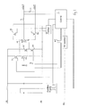
- FIG. 1 illustrates a power converter controlled by a control circuit on the secondary side.
- FIGS. 2 a and 2 b show two different power converters comprising input voltage monitoring circuitry according to a first and a second embodiment of the present invention.
- FIG. 3 shows a current generator that may be used to compensate for an offset output voltage.
- FIG. 4 shows how a differential amplifier may be used to compensate for the offset output voltage.
- FIG. 5 is a simplified block diagram of a prior art solution.
- FIGS. 6 a - 6 d illustrate the variation with time of the voltage at four different points on the secondary side.
- FIGS. 7 a - 7 c illustrate the input voltage, and the voltage over the energy storage device, according to the invention and in a prior art solution, respectively.
- FIG. 1 illustrates a power converter controlled by a control circuit on the secondary side.
- the power converter comprises a main transformer M 1 controlled by a number of switch elements S 1 , S 2 , S 3 , S 4 on the primary side.
- the switch elements are controlled by a primary side driver unit 3 .
- On the secondary side two rectifying elements R 1 , R 2 are connected to opposite ends of the secondary winding.
- the rectifying elements R 1 , R 2 are controlled by a secondary side driver unit 5 .
- the output voltage is extracted between a centre tap of the secondary winding and one of the rectification elements using an inductor L 1 and a capacitor C 1 in a way common in the art.
- the control unit 1 is connected to the primary side driver unit through a second transformer M 2 and to the secondary side driver unit 5 .
- the control unit 1 is also connected on the output from the secondary side, between the inductor L 1 and the capacitor C 1 .
- An auxiliary converter 7 is provided to bias the control circuit 1 .
- the auxiliary converter 7 is connected to the primary side driver unit 3 , the secondary side driver unit 5 and to the control unit 1 .
- the invention relates to embodiments of this auxiliary converter 7 , which will be discussed in the following.
- FIG. 2 a is a circuit diagram of a power converter comprising input voltage monitoring circuitry according to an embodiment of the present invention.
- FIG. 2 a illustrates a flyback converter but the concept can be used in any converter where the actual input voltage is transformed linearly across the insulation barrier.
- the power converter comprises a transformer TR 1 having a primary side with a primary winding and a secondary side with a secondary winding, with an insulation barrier between them.
- a voltage source Vin is arranged to provide an input voltage to the primary winding.
- a switch element in the form of a MOSFET T 1 is arranged between the voltage source and one end of the primary winding, to control the function of the transformer.
- the transformer TR 1 transforms the flyback energy to the secondary side.
- a rectification element in the form of a diode D 1 is arranged between the negative of the secondary winding and ground.
- An output voltage capacitor C 4 is connected between the other end of the secondary winding and ground to store the flyback energy. Observe the placement in the negative branch of the rectification element (diode) D 1 .
- the input voltage is to be sampled and monitored on the secondary other side of the insulation barrier.
- a number of components are arranged on the secondary side.
- One end of a first capacitor C 1 is connected to the positive end of the secondary winding.
- a first resistor R 1 is connected between the other end of the first capacitor C 1 and the negative end of the secondary winding, so that the first capacitor C 1 and the first resistor R 1 together form a derivating net.
- the gate of a second transistor T 2 is connected between the first capacitor C 1 and the first resistor R 1 .
- the source of the second transistor T 2 is connected to the negative end of the secondary winding.
- a first Zener diode DZ 1 is connected.
- a third capacitor C 2 is connected between the gate and the source of the third transistor T 3 .
- the second capacitor is provided to prevent false turn-on during the falling edge of the transformer voltage.
- a second resistor R 2 is connected in parallel with the second capacitor.
- a third resistor R 3 is connected between the second resistor R 2 and the drain of the second transistor T 2 .
- a third capacitor C 3 is connected in parallel with the connection from the source of the second transistor T 2 through the third R 3 and second R 2 resistors.
- one terminal of the third capacitor C 3 will be connected to the positive terminal of the output voltage capacitor C 4 .
- an output voltage Ucc will be provided.
- a reference voltage Uff for the control circuit will be provided.
- the derivating net comprising the first capacitor C 1 and the first resistor R 1 will sense the rising edge of the transformer voltage and cause the second transistor T 2 to conduct for a time depending on the time constant R 1 *(C 1 +CissT 2 ) and on the voltage level of the transformed voltage.
- the voltage level on the gate of the second transistor T 2 will depend on the ratio between a transistor capacitance CissT 2 and the first capacitance C 1 , Ciss being the sum of the capacitance CGS between the gate and source of the second transistor and the capacitance CDG between the drain and the gate of the second transistor.
- the second transistor T 2 will then pull down the node between the third resistor R 3 and the second transistor T 2 to the output voltage Ucc and subsequently charge the gate of the third transistor T 3 to the voltage level (Uff ⁇ Ucc)/(1+R 3 /R 2 ).
- the charge time depends mainly on the time constant of (R 2 //R 3 )*(C 2 +CissT 3 ) and the discharge time on R 2 *(C 2 +CissT 3 ).
- the third transistor T 3 will then conduct for a period as will be discussed in the following. During this time the third capacitor C 3 will be charged to the voltage over the transformer.
- the Zener diodes DZ 1 and DZ 2 are optional but useful if the input voltage has a wide range. In this case, the voltage over the gates of the second transistor T 2 and/or the third transistor T 3 can be limited by placing a Zener diode between the gate and source of each respective device. This will enable the respective transistor T 2 , T 3 to handle higher input voltages to the transformer TR 1 . Using standard devices the system can handle input voltages varying with a factor two.
- the voltage over the third capacitor C 3 will correspond to Vin*N 2 /N 1 .
- the reference voltage node Uff will have an offset of Ucc compared to GND. This offset can be removed using a current generator as shown in FIG. 3 or a differential amplifier as shown in FIG. 4 , to be connected to the output voltages of FIG. 2 a as will be discussed in more detail in the following.
- FIG. 2 b is a circuit diagram of a power converter comprising input voltage monitoring circuitry according to another embodiment of the present invention.
- FIG. 2 b illustrates a forward converter.
- the power converter comprises a transformer TR 1 having a primary side with a primary winding and a secondary side with a secondary winding, with an insulation barrier between the sides.
- a voltage source Vin is arranged to provide an input voltage to the primary winding.
- a switch element in the form of a MOSFET T 1 is arranged between the voltage source and one end of the primary winding, to control the function of the transformer.
- the transformer TR 1 transforms the energy to the secondary side.
- a first diode D 1 is connected by its anode to one end of the secondary winding.
- a second diode D 2 is connected by its anode to the other end of the secondary winding and to ground.
- the cathodes of the diodes D 1 , D 2 are interconnected. Between the interconnected cathodes and ground a first inductor L 1 and an output capacitor C 4 are connected. The output voltage Ucc is obtained across the output capacitor C 4 .
- the input voltage is to be sampled and monitored on the secondary other side of the insulation barrier.
- a number of components are arranged on the secondary side.
- One end of a first capacitor C 1 is connected between the anode of the first diode D 1 and the end of the secondary winding.
- the other end of the first capacitor C 1 is connected to the gate of a second transistor T 2 .
- a first resistor R 1 is connected between the emitter and the gate of the second transistor T 2 , and a first Zener diode DZ 1 is preferably connected in parallel with the first resistor R 1 , with its cathode connected to the gate of the transistor T 2 .
- a third transistor T 3 is also connected.
- a second resistor R 2 and a second capacitor C 2 are connected in parallel between the gate and the emitter of the third transistor T 3 .
- a second Zener diode DZ 2 is preferably connected by its anode to the gate and by its cathode to the emitter of the third transistor, in parallel with the second resistor R 2 and the second capacitor C 2 .
- the gate of the third transistor T 3 is connected to the drain of the second transistor T 2 through a third resistor R 3 .
- a third capacitor C 3 is connected between ground and the point connecting the emitter of the third transistor T 3 , the cathode of the second Zener diode and the other ends of the second capacitor C 2 and the second resistor R 2 .
- the reference voltage Uff relative to ground is obtained across the third capacitor C 3 .
- the base of a first bipolar transistor is connected to the first output voltage Ucc.
- a fourth resistor R 4 is connected between the emitter of the fourth transistor and the second output voltage Uff.
- a fifth resistor R 5 is connected between the collector of the fourth transistor T 4 and ground.
- the reference ground voltage UffGNDRef is obtained on the collector of the first bipolar transistor T 4 .
- the first bipolar transistor serves as a current generator controlled by the reference voltage Uff. This is a simple solution but may not be sufficiently exact for all implementations. This device can also be used to filter the signal by placing a capacitor over the resistors R 5 .
- FIG. 4 illustrates how a differential amplifier U 1 can be applied to remove the offset to the second voltage output Uff.
- the non-inverting input of the differential amplifier U 1 is connected through a sixth resistor R 6 to the second voltage output Uff and through a seventh resistor R 7 to ground.
- the inverting input of the differential amplifier is connected to the first voltage output Ucc through a ninth resistor R 9 .
- An eighth resistor R 8 is connected from the inverting input to the output of the differential amplifier U 1 .
- the reference ground voltage UffGNDRef is obtained on the output of the differential amplifier U 1 .
- This device can also be used to filter the signal by placing capacitors over the resistors R 7 and R 8 .
- FIG. 5 is a simplified block diagram of a prior art solution.
- a power converter comprises a transformer TR 21 having a primary side with a primary winding and a secondary side with a secondary winding, with an insulation barrier between them.
- a voltage source Vin is arranged to provide an input voltage to the primary winding.
- a switch element in the form of a MOSFET T 21 is arranged between the voltage source and one end of the primary winding, to control the function of the transformer.
- a rectifying element in the form of a diode D 11 is connected with its cathode towards the second winding.
- a number of components have been arranged in connection with the secondary winding.
- a second diode D 21 is connected with its anode towards the winding.
- a first resistor R 11 is serially connected.
- a first end of a capacitor C 13 is connected at the other end of the resistor R 11 .
- the second end of the capacitor C 13 is connected to the negative end of the secondary winding, that is, to the output voltage Vcc.
- the reference voltage node Uff is then connected to an offset compensating system, as described above with reference to FIG. 3 and FIG. 4 , which is designed to draw a current large enough to deplete the capacitor C 3 . In the case of a forward converter this is done trough a resistive divider which adjusts the signal level.
- FIGS. 6 a - 6 d illustrate a simulation of how the voltages in different points of the circuit vary with time.
- FIG. 6 a shows the voltage difference between the reference voltage Uff and the output voltage Ucc, that is, the voltage over the energy storage device C 3 .
- the ripple seen is caused by the switching of the transistors T 2 and T 3 and the charging of C 3 from the transformer T 1 .
- FIG. 6 b shows the voltage at the point of connection of the drain of the third transistor to the first diode D 1 , that is the point denoted Usw in FIGS. 2 a and 2 b .
- the figure illustrates the behaviour of a flyback converter.
- a forward type converter will have a similar appearance but, if arranged as shown in FIG. 2 b , an average voltage of zero, that is, there will be no Ucc offset.
- FIG. 6 c shows the voltage difference between the gate voltage of the second transistor T 2 , that is, the point denoted Utrig in FIGS. 2 a and 2 b , and the output voltage Ucc. This is the signal that causes the second transistor T 2 to conduct and charge C 2 +CissT 3 .
- FIG. 6 d shows the voltage difference between the gate voltage of the third transistor T 3 , that is, the point denoted Usamp in FIGS. 2 a and 2 b , and the reference voltage Uff. This signal indicates when the transistor T 3 is conducting. As can be seen there is a slight delay between this signal and the rising edge of the transformer voltage. This is enough to avoid sampling the ringing in the switch node Usw.
- FIG. 7 a illustrates the variation of the input voltage Vin to the primary side of the transformer with time.
- FIG. 7 b illustrates the variation of the reference voltage Uff relative to the output voltage Ucc with time using circuitry according to an embodiment of the invention on the secondary side.
- FIG. 7 c illustrates the variation of the reference voltage Uff relative to the output voltage Ucc with time in a prior art system.
- the prior art system has been dimensioned in such a way that the ripple on the reference voltage node matches the sampler, that is, it has been dimensioned for high accuracy rather than to have a high bandwidth.
- the same time scale is used in all three Figures.
- the curve in FIG. 7 b reflects the curve in FIG. 7 a much better than the curve in FIG. 7 c does.
Landscapes
- Engineering & Computer Science (AREA)
- Power Engineering (AREA)
- Dc-Dc Converters (AREA)
Abstract
Description
Claims (9)
Applications Claiming Priority (1)
| Application Number | Priority Date | Filing Date | Title |
|---|---|---|---|
| PCT/SE2008/050723 WO2009154523A1 (en) | 2008-06-17 | 2008-06-17 | A power converter |
Publications (2)
| Publication Number | Publication Date |
|---|---|
| US20110090724A1 US20110090724A1 (en) | 2011-04-21 |
| US8300432B2 true US8300432B2 (en) | 2012-10-30 |
Family
ID=41434278
Family Applications (1)
| Application Number | Title | Priority Date | Filing Date |
|---|---|---|---|
| US12/997,022 Expired - Fee Related US8300432B2 (en) | 2008-06-17 | 2008-06-17 | Power converter utilizing a RC circuit to conduct during the rising edge of the transformer voltage |
Country Status (4)
| Country | Link |
|---|---|
| US (1) | US8300432B2 (en) |
| EP (1) | EP2289159B1 (en) |
| CN (1) | CN102067427B (en) |
| WO (1) | WO2009154523A1 (en) |
Cited By (4)
| Publication number | Priority date | Publication date | Assignee | Title |
|---|---|---|---|---|
| US20130003422A1 (en) * | 2010-03-30 | 2013-01-03 | Telefonaktiebolaget Lm Ericsson (Publ) | Switched mode power supply with voltage regulator |
| US9985540B2 (en) | 2016-02-18 | 2018-05-29 | Telefonaktiebolaget Lm Ericsson (Publ) | Reference voltage generator for a switched mode power supply |
| US11063589B1 (en) * | 2020-04-27 | 2021-07-13 | GaN Force Corporation | Power circuit facilitating the operation of a high electron mobility transistor |
| EP4633029A1 (en) * | 2024-04-08 | 2025-10-15 | Hamilton Sundstrand Corporation | High voltage direct current bus monitoring for motor drive applications |
Families Citing this family (9)
| Publication number | Priority date | Publication date | Assignee | Title |
|---|---|---|---|---|
| US20150131350A1 (en) * | 2012-04-18 | 2015-05-14 | Takuya Isomura | Electrical power converter |
| US9071152B2 (en) | 2012-07-03 | 2015-06-30 | Cognipower, Llc | Power converter with demand pulse isolation |
| US9374011B2 (en) * | 2013-01-22 | 2016-06-21 | Power Integrations, Inc. | Secondary controller for use in synchronous flyback converter |
| CN104038050B (en) * | 2013-03-08 | 2016-09-14 | 乐星产电(无锡)有限公司 | Busbar voltage sampling apparatus |
| CN105960752A (en) * | 2014-03-11 | 2016-09-21 | 瑞典爱立信有限公司 | Isolated fly-buck converter, switched mode power supply, and method of measuring a voltage on a secondary side of an isolated fly-buck converter |
| US9819277B2 (en) * | 2015-07-09 | 2017-11-14 | Telefonaktiebolaget Lm Ericsson (Publ) | Isolated buck converter, switched mode power supply, and method of transferring digital data from a primary side to an isolated secondary side of an isolated buck converter |
| WO2018033771A1 (en) | 2016-08-16 | 2018-02-22 | Telefonaktiebolaget Lm Ericsson (Publ) | Power converter to produce a reference voltage and method of operating the same |
| US10277107B1 (en) * | 2017-12-27 | 2019-04-30 | Stmicroelectronics S.R.L. | Synchronous rectifier gate driver with active clamp |
| EP3800773A1 (en) * | 2019-10-01 | 2021-04-07 | Siemens Aktiengesellschaft | Flyback converter with determination of primary voltage in secondary circuit |
Citations (16)
| Publication number | Priority date | Publication date | Assignee | Title |
|---|---|---|---|---|
| US5663877A (en) * | 1993-07-14 | 1997-09-02 | Melcher, Ag | Synchronous rectifier that is impervious to reverse feed |
| US5708571A (en) * | 1995-09-13 | 1998-01-13 | Nec Corporation | Synchronous rectifying circuit of an active clamping type with less driving loss and less continuity loss |
| US5734563A (en) * | 1995-06-01 | 1998-03-31 | Nec Corporation | Synchronous rectification type converter |
| US6091616A (en) * | 1998-10-21 | 2000-07-18 | Lucent Technologies Inc. | Drive compensation circuit for synchronous rectifier and method of operating the same |
| US6104623A (en) * | 1999-10-21 | 2000-08-15 | Lucent Technologies, Inc. | Multiple output converter having secondary regulator using self-driven synchronous rectifiers |
| US6243278B1 (en) * | 2000-04-04 | 2001-06-05 | Tyco Electronics Logistics A.G. | Drive circuit for synchronous rectifier and method of operating the same |
| US6377477B1 (en) * | 1999-07-16 | 2002-04-23 | University Of Hong Kong | Self-driven synchronous rectifier by retention of gate charge |
| US6452818B1 (en) * | 2001-08-27 | 2002-09-17 | Anastasios A. Simopoulos | Self driven active clamp |
| USRE37889E1 (en) * | 1993-04-29 | 2002-10-22 | Lucent Technologies Inc. | Low loss synchronous rectifier for application to clamped-mode power converters |
| US6563719B1 (en) * | 2002-04-09 | 2003-05-13 | Bel-Fuse, Inc. | Self-driven synchronous rectification scheme |
| US6674658B2 (en) * | 2001-02-09 | 2004-01-06 | Netpower Technologies, Inc. | Power converter including circuits for improved operational control of synchronous rectifiers therein |
| US6831847B2 (en) * | 2000-11-20 | 2004-12-14 | Artesyn Technologies, Inc. | Synchronous rectifier drive circuit and power supply including same |
| US6987679B2 (en) * | 2003-06-18 | 2006-01-17 | Delta Electronics, Inc. | Multiple output converter with improved cross regulation |
| US7035120B2 (en) * | 2002-06-05 | 2006-04-25 | Shindengen Electric Manufacturing Co., Ltd. | Driving circuit employing synchronous rectifier circuit |
| US7751213B2 (en) * | 2008-05-20 | 2010-07-06 | Harris Corporation | Self-driven synchronous rectifier |
| US20100182807A1 (en) * | 2009-01-21 | 2010-07-22 | Funai Electric Co., Ltd. | Synchronous Rectifier Circuit Capable of Preventing Flow-Through Current |
Family Cites Families (9)
| Publication number | Priority date | Publication date | Assignee | Title |
|---|---|---|---|---|
| DK141060B (en) * | 1976-06-10 | 1979-12-31 | Rovsing As Christian | Voltage control circuit for a DC converter. |
| JP2819932B2 (en) * | 1992-03-05 | 1998-11-05 | 日本電気株式会社 | MOSFET rectifier circuit of forward converter |
| US5456511A (en) * | 1994-08-03 | 1995-10-10 | Webber; Albert F. | Truck bed extender |
| US6456511B1 (en) * | 2000-02-17 | 2002-09-24 | Tyco Electronics Corporation | Start-up circuit for flyback converter having secondary pulse width modulation |
| JP4218862B2 (en) * | 2002-03-29 | 2009-02-04 | パイオニア株式会社 | Synchronous rectifier circuit for flyback converter |
| JP2006527980A (en) * | 2003-06-19 | 2006-12-07 | コーニンクレッカ フィリップス エレクトロニクス エヌ ヴィ | Switch mode power circuit |
| US7692469B2 (en) * | 2005-04-14 | 2010-04-06 | Semiconductor Components Industries, Llc | Voltage sense circuit and method therefor |
| WO2007091374A1 (en) * | 2006-02-09 | 2007-08-16 | Murata Manufacturing Co., Ltd. | Synchronous rectification type forward converter |
| US8599833B2 (en) * | 2006-10-23 | 2013-12-03 | Telefonaktiebolaget L M Ericsson (Publ) | Transport of connectivity status information in an IP multimedia subsystem network |
-
2008
- 2008-06-17 US US12/997,022 patent/US8300432B2/en not_active Expired - Fee Related
- 2008-06-17 CN CN2008801299827A patent/CN102067427B/en not_active Expired - Fee Related
- 2008-06-17 EP EP08767189.7A patent/EP2289159B1/en not_active Not-in-force
- 2008-06-17 WO PCT/SE2008/050723 patent/WO2009154523A1/en not_active Ceased
Patent Citations (17)
| Publication number | Priority date | Publication date | Assignee | Title |
|---|---|---|---|---|
| USRE37889E1 (en) * | 1993-04-29 | 2002-10-22 | Lucent Technologies Inc. | Low loss synchronous rectifier for application to clamped-mode power converters |
| US5663877A (en) * | 1993-07-14 | 1997-09-02 | Melcher, Ag | Synchronous rectifier that is impervious to reverse feed |
| US5734563A (en) * | 1995-06-01 | 1998-03-31 | Nec Corporation | Synchronous rectification type converter |
| US5708571A (en) * | 1995-09-13 | 1998-01-13 | Nec Corporation | Synchronous rectifying circuit of an active clamping type with less driving loss and less continuity loss |
| US6091616A (en) * | 1998-10-21 | 2000-07-18 | Lucent Technologies Inc. | Drive compensation circuit for synchronous rectifier and method of operating the same |
| US6288920B1 (en) * | 1998-10-21 | 2001-09-11 | Mark E. Jacobs | Drive compensation circuit for synchronous rectifier and method of operating the same |
| US6377477B1 (en) * | 1999-07-16 | 2002-04-23 | University Of Hong Kong | Self-driven synchronous rectifier by retention of gate charge |
| US6104623A (en) * | 1999-10-21 | 2000-08-15 | Lucent Technologies, Inc. | Multiple output converter having secondary regulator using self-driven synchronous rectifiers |
| US6243278B1 (en) * | 2000-04-04 | 2001-06-05 | Tyco Electronics Logistics A.G. | Drive circuit for synchronous rectifier and method of operating the same |
| US6831847B2 (en) * | 2000-11-20 | 2004-12-14 | Artesyn Technologies, Inc. | Synchronous rectifier drive circuit and power supply including same |
| US6674658B2 (en) * | 2001-02-09 | 2004-01-06 | Netpower Technologies, Inc. | Power converter including circuits for improved operational control of synchronous rectifiers therein |
| US6452818B1 (en) * | 2001-08-27 | 2002-09-17 | Anastasios A. Simopoulos | Self driven active clamp |
| US6563719B1 (en) * | 2002-04-09 | 2003-05-13 | Bel-Fuse, Inc. | Self-driven synchronous rectification scheme |
| US7035120B2 (en) * | 2002-06-05 | 2006-04-25 | Shindengen Electric Manufacturing Co., Ltd. | Driving circuit employing synchronous rectifier circuit |
| US6987679B2 (en) * | 2003-06-18 | 2006-01-17 | Delta Electronics, Inc. | Multiple output converter with improved cross regulation |
| US7751213B2 (en) * | 2008-05-20 | 2010-07-06 | Harris Corporation | Self-driven synchronous rectifier |
| US20100182807A1 (en) * | 2009-01-21 | 2010-07-22 | Funai Electric Co., Ltd. | Synchronous Rectifier Circuit Capable of Preventing Flow-Through Current |
Cited By (5)
| Publication number | Priority date | Publication date | Assignee | Title |
|---|---|---|---|---|
| US20130003422A1 (en) * | 2010-03-30 | 2013-01-03 | Telefonaktiebolaget Lm Ericsson (Publ) | Switched mode power supply with voltage regulator |
| US8964416B2 (en) * | 2010-03-30 | 2015-02-24 | Telefonaktiebolaget L M Ericsson (Publ) | Switched mode power supply with voltage regulator |
| US9985540B2 (en) | 2016-02-18 | 2018-05-29 | Telefonaktiebolaget Lm Ericsson (Publ) | Reference voltage generator for a switched mode power supply |
| US11063589B1 (en) * | 2020-04-27 | 2021-07-13 | GaN Force Corporation | Power circuit facilitating the operation of a high electron mobility transistor |
| EP4633029A1 (en) * | 2024-04-08 | 2025-10-15 | Hamilton Sundstrand Corporation | High voltage direct current bus monitoring for motor drive applications |
Also Published As
| Publication number | Publication date |
|---|---|
| CN102067427B (en) | 2013-12-25 |
| EP2289159A4 (en) | 2016-12-14 |
| EP2289159A1 (en) | 2011-03-02 |
| EP2289159B1 (en) | 2019-01-30 |
| WO2009154523A1 (en) | 2009-12-23 |
| CN102067427A (en) | 2011-05-18 |
| US20110090724A1 (en) | 2011-04-21 |
Similar Documents
| Publication | Publication Date | Title |
|---|---|---|
| US8300432B2 (en) | Power converter utilizing a RC circuit to conduct during the rising edge of the transformer voltage | |
| US8953347B2 (en) | Capacitor discharging circuit and power converter | |
| CN103066872B (en) | Integration switch power supply controller and switch power supply using the same | |
| US8416596B2 (en) | Switching power controller and system | |
| US8400789B2 (en) | Power supply with input filter-controlled switch clamp circuit | |
| US9455635B2 (en) | Snubber circuit and buffering method for snubber circuit | |
| US20110261596A1 (en) | Control circuit for primary side control of switching power supply | |
| CN102447394B (en) | Flyback converter with an adaptively controlled rectifier arrangement | |
| US6473317B1 (en) | Forward DC/DC converter with semi-synchronous rectification and improved efficiency | |
| US11509227B2 (en) | Active clamp flyback converter | |
| CN103200738A (en) | Constant current drive controller and light-emitting diode (LED) constant current drive circuit | |
| CN110504832B (en) | Control circuit and method for high-voltage BUCK switch converter | |
| US9729073B1 (en) | Power conversion apparatus | |
| CN119497953A (en) | Power modules, routers, switches and electronic devices | |
| US20240014727A1 (en) | Power control device and flyback converter | |
| US9397575B2 (en) | Switching power supply device | |
| WO2017140368A1 (en) | Reference voltage generator for a switched mode power supply | |
| CN208608900U (en) | Electric power converter control circuit | |
| Chakraborty et al. | An improved asymmetric half-bridge converter with zero DC offset of magnetizing current | |
| CN114710044B (en) | Flyback converter and constant current control method thereof | |
| CN110504842B (en) | Quasi-resonance control circuit and valley bottom opening method thereof | |
| CN121485450B (en) | A protection circuit, method, chip, flyback converter, and switching power supply | |
| Fan et al. | A high-voltage low-power switched-capacitor DC-DC converter based on GaN and SiC devices for LED drivers | |
| CN224218287U (en) | A power control chip with variable sampling blanking time | |
| CN117318500B (en) | Power conversion system, control method of power converter, power supply and electronic device |
Legal Events
| Date | Code | Title | Description |
|---|---|---|---|
| AS | Assignment |
Owner name: TELEFONAKTIEBOLAGET LM ERICSSON (PUBL), SWEDEN Free format text: ASSIGNMENT OF ASSIGNORS INTEREST;ASSIGNOR:APPELBERG, MIKAEL;REEL/FRAME:025636/0487 Effective date: 20080811 |
|
| ZAAA | Notice of allowance and fees due |
Free format text: ORIGINAL CODE: NOA |
|
| ZAAB | Notice of allowance mailed |
Free format text: ORIGINAL CODE: MN/=. |
|
| STCF | Information on status: patent grant |
Free format text: PATENTED CASE |
|
| CC | Certificate of correction | ||
| FPAY | Fee payment |
Year of fee payment: 4 |
|
| MAFP | Maintenance fee payment |
Free format text: PAYMENT OF MAINTENANCE FEE, 8TH YEAR, LARGE ENTITY (ORIGINAL EVENT CODE: M1552); ENTITY STATUS OF PATENT OWNER: LARGE ENTITY Year of fee payment: 8 |
|
| FEPP | Fee payment procedure |
Free format text: MAINTENANCE FEE REMINDER MAILED (ORIGINAL EVENT CODE: REM.); ENTITY STATUS OF PATENT OWNER: LARGE ENTITY |
|
| LAPS | Lapse for failure to pay maintenance fees |
Free format text: PATENT EXPIRED FOR FAILURE TO PAY MAINTENANCE FEES (ORIGINAL EVENT CODE: EXP.); ENTITY STATUS OF PATENT OWNER: LARGE ENTITY |
|
| STCH | Information on status: patent discontinuation |
Free format text: PATENT EXPIRED DUE TO NONPAYMENT OF MAINTENANCE FEES UNDER 37 CFR 1.362 |
|
| FP | Lapsed due to failure to pay maintenance fee |
Effective date: 20241030 |