US8278736B2 - Electrostatic discharge protection device - Google Patents
Electrostatic discharge protection device Download PDFInfo
- Publication number
- US8278736B2 US8278736B2 US12/875,217 US87521710A US8278736B2 US 8278736 B2 US8278736 B2 US 8278736B2 US 87521710 A US87521710 A US 87521710A US 8278736 B2 US8278736 B2 US 8278736B2
- Authority
- US
- United States
- Prior art keywords
- doped region
- type doped
- protection device
- type
- field oxide
- Prior art date
- Legal status (The legal status is an assumption and is not a legal conclusion. Google has not performed a legal analysis and makes no representation as to the accuracy of the status listed.)
- Active, expires
Links
- 238000010586 diagram Methods 0.000 description 18
- 238000007796 conventional method Methods 0.000 description 3
- 238000000034 method Methods 0.000 description 2
- 238000012986 modification Methods 0.000 description 2
- 230000004048 modification Effects 0.000 description 2
- 239000004065 semiconductor Substances 0.000 description 2
- XUIMIQQOPSSXEZ-UHFFFAOYSA-N Silicon Chemical compound [Si] XUIMIQQOPSSXEZ-UHFFFAOYSA-N 0.000 description 1
- 239000003990 capacitor Substances 0.000 description 1
- 230000015556 catabolic process Effects 0.000 description 1
- 238000004519 manufacturing process Methods 0.000 description 1
- 229910052710 silicon Inorganic materials 0.000 description 1
- 239000010703 silicon Substances 0.000 description 1
Images


Classifications
-
- H—ELECTRICITY
- H10—SEMICONDUCTOR DEVICES; ELECTRIC SOLID-STATE DEVICES NOT OTHERWISE PROVIDED FOR
- H10D—INORGANIC ELECTRIC SEMICONDUCTOR DEVICES
- H10D89/00—Aspects of integrated devices not covered by groups H10D84/00 - H10D88/00
- H10D89/60—Integrated devices comprising arrangements for electrical or thermal protection, e.g. protection circuits against electrostatic discharge [ESD]
- H10D89/601—Integrated devices comprising arrangements for electrical or thermal protection, e.g. protection circuits against electrostatic discharge [ESD] for devices having insulated gate electrodes, e.g. for IGFETs or IGBTs
- H10D89/711—Integrated devices comprising arrangements for electrical or thermal protection, e.g. protection circuits against electrostatic discharge [ESD] for devices having insulated gate electrodes, e.g. for IGFETs or IGBTs using bipolar transistors as protective elements
-
- H—ELECTRICITY
- H10—SEMICONDUCTOR DEVICES; ELECTRIC SOLID-STATE DEVICES NOT OTHERWISE PROVIDED FOR
- H10D—INORGANIC ELECTRIC SEMICONDUCTOR DEVICES
- H10D89/00—Aspects of integrated devices not covered by groups H10D84/00 - H10D88/00
- H10D89/60—Integrated devices comprising arrangements for electrical or thermal protection, e.g. protection circuits against electrostatic discharge [ESD]
- H10D89/601—Integrated devices comprising arrangements for electrical or thermal protection, e.g. protection circuits against electrostatic discharge [ESD] for devices having insulated gate electrodes, e.g. for IGFETs or IGBTs
- H10D89/811—Integrated devices comprising arrangements for electrical or thermal protection, e.g. protection circuits against electrostatic discharge [ESD] for devices having insulated gate electrodes, e.g. for IGFETs or IGBTs using FETs as protective elements
- H10D89/813—Integrated devices comprising arrangements for electrical or thermal protection, e.g. protection circuits against electrostatic discharge [ESD] for devices having insulated gate electrodes, e.g. for IGFETs or IGBTs using FETs as protective elements specially adapted to provide an electrical current path other than the field-effect induced current path
- H10D89/814—Integrated devices comprising arrangements for electrical or thermal protection, e.g. protection circuits against electrostatic discharge [ESD] for devices having insulated gate electrodes, e.g. for IGFETs or IGBTs using FETs as protective elements specially adapted to provide an electrical current path other than the field-effect induced current path involving a parasitic bipolar transistor triggered by the electrical biasing of the gate electrode of the FET, e.g. gate coupled transistors
Definitions
- the invention relates to a protection device, and more particularly to an electrostatic discharge (ESD) protection device receiving high operation voltage.
- ESD electrostatic discharge
- ESD protection has become one of the most critical reliability issues for integrated circuits (IC).
- IC integrated circuits
- scaled-down devices and thinner gate oxides are more vulnerable to ESD stress.
- a conventional method is to integrate an ESD protection device in ICs.
- Vh holding voltage
- Vtl trigger voltages
- the holding voltage is typically less than the operation voltage (VDD).
- VDD operation voltage
- a latch-up problem may occur.
- a conventional method used is to increase the holding voltage.
- the trigger voltage of the ESD protection device is also increased when the holding voltage is increased. Thus, reducing the efficiency of the ESD protection device.
- FIG. 1 is a schematic diagram of a conventional GGNMOS.
- FIG. 2 is a schematic diagram of a conventional N-type SCR.
- FIG. 3A is a schematic diagram of a conventional series GGNMOS.
- FIG. 3B is an equivalent circuit of the conventional series GGNMOS shown in FIG. 3A . Since the GGNMOSs are connected in series, the holding voltage of the ESD protection device can be increased.
- the trigger voltage of the ESD protection device is also increased when the holding voltage is increased.
- a resistor R and a capacitor C are utilized to reduce the trigger voltage of the ESD protection device.
- FIG. 3C is a characteristic diagram of the series GGNMOS shown in FIG. 3A .
- the curve 31 represents a relationship between the voltage and the current of the series GGNMOS shown in FIG. 3A .
- the curve 32 represents a relationship between the voltage and the leakage current of the series GGNMOS shown in FIG. 3A .
- leakage current of a series GGNMOS is suddenly increased when snapback breakdown occurs.
- an electrostatic discharge protection device is coupled between a first power line and a second power line and comprises a P-type well, a first N-type doped region, a first P-type doped region, a second P-type doped region and a second N-type doped region.
- the first N-type doped region is formed in the P-type well.
- the first P-type doped region is formed in the first N-type doped region.
- the second P-type doped region comprises a first portion and a second portion. The first portion of the second P-type doped region is formed in the first N-type doped region.
- the second portion of the second P-type doped region is formed outside of the first N-type doped region.
- the second N-type doped region is formed in the first portion of the second P-type doped region.
- the first P-type doped region, the first N-type doped region, the second P-type doped region and the second N-type doped region constitute an insulated gate bipolar transistor (IGBT).
- IGBT insulated gate bipolar transistor
- FIG. 1 is a schematic diagram of a conventional GGNMOS
- FIG. 2 is a schematic diagram of a conventional N-type SCR
- FIG. 3A is a schematic diagram of a conventional series GGNMOS
- FIG. 3B is an equivalent circuit of the conventional series GGNMOS shown in FIG. 3A ;
- FIG. 3C is a characteristic diagram of the series GGNMOS shown in FIG. 3A ;
- FIG. 4A is a schematic diagram of an exemplary embodiment of an ESD protection device
- FIG. 4B is a schematic diagram of another exemplary embodiment of an ESD protection device
- FIG. 5A is a schematic diagram of another exemplary embodiment of an ESD protection device
- FIG. 5B is a schematic diagram of another exemplary embodiment of an ESD protection device.
- FIG. 6 is a characteristic diagram of the ESD protection device of the invention.
- FIG. 4A is a schematic diagram of an exemplary embodiment of an ESD protection device.
- the ESD protection device 400 is an insulated gate bipolar transistor (IGBT).
- the IGBT is formed by a P-type doped region 431 , an N-type doped region 421 , a P-type doped region 432 and an N-type doped region 422 .
- an ESD current flows from the P-type doped region 431 , the N-type doped region 421 , the P-type doped region 432 and the N-type doped region 422 to the power line 452 .
- the N-type doped region 421 is formed in the P-type well 410 .
- the N-type doped region 421 is a well and is capable of sustaining high operation voltage.
- the N-type doped region 421 can be referred to as a high voltage N-type well (HVNW).
- the P-type doped region 431 is formed in the N-type doped region 421 .
- the P-type doped region 431 is a heavily doped region and coupled to the power line 451 .
- the symbol P+ represents a heavily doped P-type region.
- the left edge of the P-type doped region 431 contacts with a field oxide 441 and the right edge of the P-type doped region 431 contacts with a field oxide 443 .
- the P-type doped region 432 comprises a first portion A 1 and a second portion A 2 .
- the first portion A 1 of the P-type doped region 432 is formed in the N-type doped region 421 .
- the second portion A 2 of the P-type doped region 432 is formed outside of the N-type doped region 421 .
- the P-type doped region 432 is also referred to as a P-body.
- the doped concentration of the P-type doped region 432 is less than the doped concentration of the P-type doped region 431 .
- the N-type doped region 422 is formed in the first portion A 1 of the P-type doped region 432 .
- the N-type doped region 422 is a heavily doped region.
- the doped concentration of the N-type doped region 422 is less than the doped concentration of the N-type doped region 421 .
- the symbol N+ represents a heavily N-type doped region.
- the ESD protection device 400 further comprises an N-type doped region 423 and a P-type doped region 433 , but the disclosure is not limited thereto. Since the doped concentration of the P-type doped region 431 is higher than the doped concentration of the N-type doped region 421 , the N-type doped region 423 is disposed between the P-type doped region 431 and the N-type doped region 421 .
- the N-type doped region 423 is an N-type drain drift (NDD).
- the doped concentration of the N-type doped region 423 is higher than the doped concentration of the N-type doped region 421 .
- a P-type doped region such as a P-type drain drift (PDD) is utilized to replace the N-type doped region 423 .
- the P-type doped region 433 is also a heavily doped region.
- the P-type doped region 433 serves as an electro-contact point of the P-type doped region 432 .
- a field oxide 442 is disposed between the P-type doped region 433 and the N-type doped region 422 .
- the N-type doped region 422 and the P-type doped region 433 are formed in the P-type doped region 432 .
- the P-type doped region 433 is disposed between a field oxide 444 and the field oxide 442 .
- the P-type doped region 431 is coupled to the power line 451 and the P-type doped region 433 and the N-type doped region 422 are coupled to the power line 452 .
- the power line 451 receives a high operation voltage VDD and the power line 452 receives a low operation voltage VSS.
- the high operation voltage VDD may be 24V and the low operation voltage VSS may be 0V, but the disclosure is not limited thereto.
- the distances S 1 , d 1 , Lgd, Lox, and P 1 are adjusted to increase the holding voltage (Vh) of the ESD protection device 400 and reduce the trigger voltage (Vtl) of the ESD protection device 400 .
- the right edge of the field oxide 441 contacts with the left side of the P-type doped region 431 and the left edge of the field oxide 443 contacts with the right side of the P-type doped region 431 .
- a leakage current is approximately 1 E- 11 A.
- the distances S 1 and d 1 are controlled so that the leakage current is reduced, wherein the reduce level is approximately 1-1.5 stages ( 7 E- 13 A).
- the invention does not limit the distances S 1 and d 1 .
- the distance S 1 is within 0.35 um-100 um and the distance d 1 is within 1 um-30 um.
- FIG. 4B is a schematic diagram of another exemplary embodiment of an ESD protection device.
- FIG. 4B is similar to FIG. 4A with the exception that the right edge of the field oxide 441 ′ does not contact with the left side of the P-type doped region 431 ′ and the left edge of the field oxide 443 does not contact with the right side of the P-type doped region 431 ′.
- a portion of the N-type doped region 423 ′ separates the field oxide 441 ′ from the P-type doped region 431 ′ and another portion of the N-type doped region 423 ′ separates the field oxide 443 from the P-type doped region 431 ′.
- a space d 2 occurs between the field oxide 441 ′ and the P-type doped region 431 ′ and another space d 2 occurs between the field oxide 443 and the P-type doped region 431 ′.
- the space d 2 and the distance d 1 ′ can be adjusted so that the leakage current is reduced, wherein the reduce level is approximately 1-1.5 stages ( 7 E- 13 A).
- the field oxides 442 ⁇ 444 of FIG. 4B are similar to the field oxides 442 ⁇ 444 of FIG. 4A , the descriptions of the field oxides 442 ⁇ 444 of FIG. 4B are omitted for brevity.
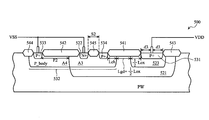
- FIG. 5A is a schematic diagram of another exemplary embodiment of an ESD protection device.
- FIG. 5A is similar to FIG. 4A except for the addition of a field oxide 545 and a P-type doped region 534 . Since the field oxides 542 ⁇ 544 of FIG. 5A are similar to the field oxides 442 ⁇ 444 of FIG. 4A , the descriptions of the field oxides 542 ⁇ 544 are omitted for brevity.
- the field oxide 545 is formed between the N-type doped region 522 and the P-type doped region 534 .
- the distance between the edges of the field oxide 545 is S 2 .
- the distance S 2 is adjusted to hinder a leakage current problem.
- the P-type doped region 532 comprises a first portion A 3 and a second portion A 4 .
- the first portion A 3 of the P-type doped region 532 is formed in the N-type doped region 521 .
- the second portion A 4 of the P-type doped region 532 is formed outside of the N-type doped region 521 .
- the P-type doped region 534 , the N-type doped region 522 and the P-type doped region 533 are formed in the P-type doped region 532 .
- the distances Lch, Lgd and Lox are adjusted to hinder a leakage current problem. Since the distances S 2 , P 2 , d 3 , Lch, Lgd and Lox are clearly shown in FIG. 5A , the defining methods of the distances S 2 , P 2 , d 3 , Lch, Lgd and Lox are omitted.
- FIG. 5B is a schematic diagram of another exemplary embodiment of an ESD protection device.
- FIG. 5B is similar to FIG. 5A with the exception that the right edge of the field oxide 541 ′ does not contact with the left side of the P-type doped region 531 ′ and the left edge of the field oxide 546 does not contact with the right side of the P-type doped region 531 ′.
- a space d 4 occurs between the field oxide 541 ′ and the P-type doped region 531 ′ and another space d 4 occurs between the field oxide 546 and the P-type doped region 531 ′.
- the space d 4 and the distance d 3 ′ can be adjusted to reduce the leakage current of the ESD protection device 500 .
- the field oxides 542 and 544 of FIG. 5B are similar to the field oxides 542 and 544 of FIG. 5A , the descriptions of the field oxides 542 and 544 are omitted for brevity.
- FIG. 6 is a characteristic diagram of the ESD protection device of the invention.
- the curve 61 represents a relationship between the voltage and the current of an ESD protection device.
- the curve 62 represents a relationship between the voltage and the leakage current of the ESD protection device. Taking FIG. 5A as an example, assuming the distance S 2 is 15 um, the distance Lch is 0.75 um, the distance Lgd is 40 um, the distance Lox is 2 um, the distance d 3 is 10 um and the distance P 2 is 15 um.
- the holding voltage of the ESD protection device 500 is approximately 33V higher than the high operation voltage VDD (24V). Further, the trigger voltage of the ESD protection device 500 is approximately 38V. As shown in the curve 62 , the leakage current of the ESD protection device 500 is maintained at a fix value.
Landscapes
- Semiconductor Integrated Circuits (AREA)
Abstract
Description
Claims (9)
Priority Applications (1)
| Application Number | Priority Date | Filing Date | Title |
|---|---|---|---|
| US12/875,217 US8278736B2 (en) | 2010-09-03 | 2010-09-03 | Electrostatic discharge protection device |
Applications Claiming Priority (1)
| Application Number | Priority Date | Filing Date | Title |
|---|---|---|---|
| US12/875,217 US8278736B2 (en) | 2010-09-03 | 2010-09-03 | Electrostatic discharge protection device |
Publications (2)
| Publication Number | Publication Date |
|---|---|
| US20120056239A1 US20120056239A1 (en) | 2012-03-08 |
| US8278736B2 true US8278736B2 (en) | 2012-10-02 |
Family
ID=45770063
Family Applications (1)
| Application Number | Title | Priority Date | Filing Date |
|---|---|---|---|
| US12/875,217 Active 2031-04-23 US8278736B2 (en) | 2010-09-03 | 2010-09-03 | Electrostatic discharge protection device |
Country Status (1)
| Country | Link |
|---|---|
| US (1) | US8278736B2 (en) |
-
2010
- 2010-09-03 US US12/875,217 patent/US8278736B2/en active Active
Also Published As
| Publication number | Publication date |
|---|---|
| US20120056239A1 (en) | 2012-03-08 |
Similar Documents
| Publication | Publication Date | Title |
|---|---|---|
| US8093623B2 (en) | Semiconductor integrated circuit | |
| CN102214655B (en) | Integrated circuit and method for reducing the trigger voltage of a stacked electrostatic discharge protection circuit | |
| US8482071B2 (en) | Diode biased ESD protection device and method | |
| US7554839B2 (en) | Symmetric blocking transient voltage suppressor (TVS) using bipolar transistor base snatch | |
| US8519434B2 (en) | Self detection device for high voltage ESD protection | |
| US10141300B1 (en) | Low capacitance transient voltage suppressor | |
| US20090032838A1 (en) | Symmetric bidirectional silicon-controlled rectifier | |
| CN103579224B (en) | ESD protects | |
| US8963288B2 (en) | ESD protection circuit | |
| US8611059B2 (en) | Power management circuit and high voltage device therein | |
| CN103715233B (en) | A kind of ESD protective device of the LDMOS structure with high maintenance voltage | |
| US8093630B2 (en) | Semiconductor device and lateral diffused metal-oxide-semiconductor transistor | |
| US10978870B2 (en) | Electrostatic discharge protection device | |
| US9633992B1 (en) | Electrostatic discharge protection device | |
| US11222888B2 (en) | Anti-static metal oxide semiconductor field effect transistor structure | |
| CN104241277B (en) | A kind of SCR device that GDPMOS is embedded with high maintenance voltage | |
| KR101488566B1 (en) | Electrostatic Discharge Protection Circuit | |
| KR101476005B1 (en) | Electrostatic Discharge Protection Circuit | |
| CN102237400B (en) | ESD protection device | |
| US8278736B2 (en) | Electrostatic discharge protection device | |
| WO2013128583A1 (en) | Semiconductor device | |
| CN108461488B (en) | Electrostatic discharge clamping device, circuit and electrostatic discharge protection circuit | |
| US8278715B2 (en) | Electrostatic discharge protection device | |
| US10121777B2 (en) | Silicon controlled rectifier | |
| TWI458091B (en) | Electrostatic discharge device |
Legal Events
| Date | Code | Title | Description |
|---|---|---|---|
| AS | Assignment |
Owner name: VANGUARD INTERNATIONAL SEMICONDUCTOR CORPORATION, Free format text: ASSIGNMENT OF ASSIGNORS INTEREST;ASSIGNORS:JOU, YEH-NING;HUNG, CHIA-WEI;CHANG, SHU-LING;AND OTHERS;REEL/FRAME:024938/0893 Effective date: 20100723 |
|
| FEPP | Fee payment procedure |
Free format text: PAT HOLDER NO LONGER CLAIMS SMALL ENTITY STATUS, ENTITY STATUS SET TO UNDISCOUNTED (ORIGINAL EVENT CODE: STOL); ENTITY STATUS OF PATENT OWNER: LARGE ENTITY |
|
| STCF | Information on status: patent grant |
Free format text: PATENTED CASE |
|
| SULP | Surcharge for late payment | ||
| FPAY | Fee payment |
Year of fee payment: 4 |
|
| MAFP | Maintenance fee payment |
Free format text: PAYMENT OF MAINTENANCE FEE, 8TH YEAR, LARGE ENTITY (ORIGINAL EVENT CODE: M1552); ENTITY STATUS OF PATENT OWNER: LARGE ENTITY Year of fee payment: 8 |
|
| MAFP | Maintenance fee payment |
Free format text: PAYMENT OF MAINTENANCE FEE, 12TH YEAR, LARGE ENTITY (ORIGINAL EVENT CODE: M1553); ENTITY STATUS OF PATENT OWNER: LARGE ENTITY Year of fee payment: 12 |