US8248584B2 - Exposure apparatus and device manufacturing method - Google Patents

Exposure apparatus and device manufacturing method Download PDF

Info

Publication number
US8248584B2
US8248584B2 US12/395,487 US39548709A US8248584B2 US 8248584 B2 US8248584 B2 US 8248584B2 US 39548709 A US39548709 A US 39548709A US 8248584 B2 US8248584 B2 US 8248584B2
Authority
US
United States
Prior art keywords
reference substrate
correction value
measurement
wafer
unit
Prior art date
Legal status (The legal status is an assumption and is not a legal conclusion. Google has not performed a legal analysis and makes no representation as to the accuracy of the status listed.)
Expired - Fee Related, expires
Application number
US12/395,487
Other versions
US20090225292A1 (en
Inventor
Masataro Shiroiwa
Hiroki Suzukawa
Current Assignee (The listed assignees may be inaccurate. Google has not performed a legal analysis and makes no representation or warranty as to the accuracy of the list.)
Canon Inc
Original Assignee
Canon Inc
Priority date (The priority date is an assumption and is not a legal conclusion. Google has not performed a legal analysis and makes no representation as to the accuracy of the date listed.)
Filing date
Publication date
Application filed by Canon Inc filed Critical Canon Inc
Assigned to CANON KABUSHIKI KAISHA reassignment CANON KABUSHIKI KAISHA ASSIGNMENT OF ASSIGNORS INTEREST (SEE DOCUMENT FOR DETAILS). Assignors: SUZUKAWA, HIROKI, SHIROIWA, MASATARO
Publication of US20090225292A1 publication Critical patent/US20090225292A1/en
Priority to US13/544,790 priority Critical patent/US20120274916A1/en
Application granted granted Critical
Publication of US8248584B2 publication Critical patent/US8248584B2/en
Expired - Fee Related legal-status Critical Current
Adjusted expiration legal-status Critical

Links

Images

Classifications

    • GPHYSICS
    • G03PHOTOGRAPHY; CINEMATOGRAPHY; ANALOGOUS TECHNIQUES USING WAVES OTHER THAN OPTICAL WAVES; ELECTROGRAPHY; HOLOGRAPHY
    • G03FPHOTOMECHANICAL PRODUCTION OF TEXTURED OR PATTERNED SURFACES, e.g. FOR PRINTING, FOR PROCESSING OF SEMICONDUCTOR DEVICES; MATERIALS THEREFOR; ORIGINALS THEREFOR; APPARATUS SPECIALLY ADAPTED THEREFOR
    • G03F7/00Photomechanical, e.g. photolithographic, production of textured or patterned surfaces, e.g. printing surfaces; Materials therefor, e.g. comprising photoresists; Apparatus specially adapted therefor
    • G03F7/70Microphotolithographic exposure; Apparatus therefor
    • G03F7/70691Handling of masks or workpieces
    • G03F7/70775Position control, e.g. interferometers or encoders for determining the stage position
    • GPHYSICS
    • G03PHOTOGRAPHY; CINEMATOGRAPHY; ANALOGOUS TECHNIQUES USING WAVES OTHER THAN OPTICAL WAVES; ELECTROGRAPHY; HOLOGRAPHY
    • G03BAPPARATUS OR ARRANGEMENTS FOR TAKING PHOTOGRAPHS OR FOR PROJECTING OR VIEWING THEM; APPARATUS OR ARRANGEMENTS EMPLOYING ANALOGOUS TECHNIQUES USING WAVES OTHER THAN OPTICAL WAVES; ACCESSORIES THEREFOR
    • G03B27/00Photographic printing apparatus
    • G03B27/32Projection printing apparatus, e.g. enlarger, copying camera
    • G03B27/42Projection printing apparatus, e.g. enlarger, copying camera for automatic sequential copying of the same original
    • GPHYSICS
    • G03PHOTOGRAPHY; CINEMATOGRAPHY; ANALOGOUS TECHNIQUES USING WAVES OTHER THAN OPTICAL WAVES; ELECTROGRAPHY; HOLOGRAPHY
    • G03FPHOTOMECHANICAL PRODUCTION OF TEXTURED OR PATTERNED SURFACES, e.g. FOR PRINTING, FOR PROCESSING OF SEMICONDUCTOR DEVICES; MATERIALS THEREFOR; ORIGINALS THEREFOR; APPARATUS SPECIALLY ADAPTED THEREFOR
    • G03F7/00Photomechanical, e.g. photolithographic, production of textured or patterned surfaces, e.g. printing surfaces; Materials therefor, e.g. comprising photoresists; Apparatus specially adapted therefor
    • G03F7/70Microphotolithographic exposure; Apparatus therefor
    • G03F7/70425Imaging strategies, e.g. for increasing throughput or resolution, printing product fields larger than the image field or compensating lithography- or non-lithography errors, e.g. proximity correction, mix-and-match, stitching or double patterning
    • GPHYSICS
    • G03PHOTOGRAPHY; CINEMATOGRAPHY; ANALOGOUS TECHNIQUES USING WAVES OTHER THAN OPTICAL WAVES; ELECTROGRAPHY; HOLOGRAPHY
    • G03FPHOTOMECHANICAL PRODUCTION OF TEXTURED OR PATTERNED SURFACES, e.g. FOR PRINTING, FOR PROCESSING OF SEMICONDUCTOR DEVICES; MATERIALS THEREFOR; ORIGINALS THEREFOR; APPARATUS SPECIALLY ADAPTED THEREFOR
    • G03F7/00Photomechanical, e.g. photolithographic, production of textured or patterned surfaces, e.g. printing surfaces; Materials therefor, e.g. comprising photoresists; Apparatus specially adapted therefor
    • G03F7/70Microphotolithographic exposure; Apparatus therefor
    • G03F7/70483Information management; Active and passive control; Testing; Wafer monitoring, e.g. pattern monitoring
    • G03F7/70491Information management, e.g. software; Active and passive control, e.g. details of controlling exposure processes or exposure tool monitoring processes
    • G03F7/70525Controlling normal operating mode, e.g. matching different apparatus, remote control or prediction of failure
    • GPHYSICS
    • G03PHOTOGRAPHY; CINEMATOGRAPHY; ANALOGOUS TECHNIQUES USING WAVES OTHER THAN OPTICAL WAVES; ELECTROGRAPHY; HOLOGRAPHY
    • G03FPHOTOMECHANICAL PRODUCTION OF TEXTURED OR PATTERNED SURFACES, e.g. FOR PRINTING, FOR PROCESSING OF SEMICONDUCTOR DEVICES; MATERIALS THEREFOR; ORIGINALS THEREFOR; APPARATUS SPECIALLY ADAPTED THEREFOR
    • G03F7/00Photomechanical, e.g. photolithographic, production of textured or patterned surfaces, e.g. printing surfaces; Materials therefor, e.g. comprising photoresists; Apparatus specially adapted therefor
    • G03F7/70Microphotolithographic exposure; Apparatus therefor
    • G03F7/70483Information management; Active and passive control; Testing; Wafer monitoring, e.g. pattern monitoring
    • G03F7/70605Workpiece metrology
    • G03F7/706843Metrology apparatus
    • G03F7/706845Calibration, e.g. tool-to-tool calibration, beam alignment, spot position or focus
    • GPHYSICS
    • G03PHOTOGRAPHY; CINEMATOGRAPHY; ANALOGOUS TECHNIQUES USING WAVES OTHER THAN OPTICAL WAVES; ELECTROGRAPHY; HOLOGRAPHY
    • G03FPHOTOMECHANICAL PRODUCTION OF TEXTURED OR PATTERNED SURFACES, e.g. FOR PRINTING, FOR PROCESSING OF SEMICONDUCTOR DEVICES; MATERIALS THEREFOR; ORIGINALS THEREFOR; APPARATUS SPECIALLY ADAPTED THEREFOR
    • G03F7/00Photomechanical, e.g. photolithographic, production of textured or patterned surfaces, e.g. printing surfaces; Materials therefor, e.g. comprising photoresists; Apparatus specially adapted therefor
    • G03F7/70Microphotolithographic exposure; Apparatus therefor
    • G03F7/70691Handling of masks or workpieces
    • G03F7/70733Handling masks and workpieces, e.g. exchange of workpiece or mask, transport of workpiece or mask
    • G03F7/7075Handling workpieces outside exposure position, e.g. SMIF box
    • GPHYSICS
    • G03PHOTOGRAPHY; CINEMATOGRAPHY; ANALOGOUS TECHNIQUES USING WAVES OTHER THAN OPTICAL WAVES; ELECTROGRAPHY; HOLOGRAPHY
    • G03FPHOTOMECHANICAL PRODUCTION OF TEXTURED OR PATTERNED SURFACES, e.g. FOR PRINTING, FOR PROCESSING OF SEMICONDUCTOR DEVICES; MATERIALS THEREFOR; ORIGINALS THEREFOR; APPARATUS SPECIALLY ADAPTED THEREFOR
    • G03F7/00Photomechanical, e.g. photolithographic, production of textured or patterned surfaces, e.g. printing surfaces; Materials therefor, e.g. comprising photoresists; Apparatus specially adapted therefor
    • G03F7/70Microphotolithographic exposure; Apparatus therefor
    • G03F7/708Construction of apparatus, e.g. environment aspects, hygiene aspects or materials
    • G03F7/7085Detection arrangement, e.g. detectors of apparatus alignment possibly mounted on wafers, exposure dose, photo-cleaning flux, stray light, thermal load
    • GPHYSICS
    • G03PHOTOGRAPHY; CINEMATOGRAPHY; ANALOGOUS TECHNIQUES USING WAVES OTHER THAN OPTICAL WAVES; ELECTROGRAPHY; HOLOGRAPHY
    • G03FPHOTOMECHANICAL PRODUCTION OF TEXTURED OR PATTERNED SURFACES, e.g. FOR PRINTING, FOR PROCESSING OF SEMICONDUCTOR DEVICES; MATERIALS THEREFOR; ORIGINALS THEREFOR; APPARATUS SPECIALLY ADAPTED THEREFOR
    • G03F7/00Photomechanical, e.g. photolithographic, production of textured or patterned surfaces, e.g. printing surfaces; Materials therefor, e.g. comprising photoresists; Apparatus specially adapted therefor
    • G03F7/70Microphotolithographic exposure; Apparatus therefor
    • G03F7/708Construction of apparatus, e.g. environment aspects, hygiene aspects or materials
    • G03F7/70991Connection with other apparatus, e.g. multiple exposure stations, particular arrangement of exposure apparatus and pre-exposure and/or post-exposure apparatus; Shared apparatus, e.g. having shared radiation source, shared mask or workpiece stage, shared base-plate; Utilities, e.g. cable, pipe or wireless arrangements for data, power, fluids or vacuum
    • GPHYSICS
    • G03PHOTOGRAPHY; CINEMATOGRAPHY; ANALOGOUS TECHNIQUES USING WAVES OTHER THAN OPTICAL WAVES; ELECTROGRAPHY; HOLOGRAPHY
    • G03FPHOTOMECHANICAL PRODUCTION OF TEXTURED OR PATTERNED SURFACES, e.g. FOR PRINTING, FOR PROCESSING OF SEMICONDUCTOR DEVICES; MATERIALS THEREFOR; ORIGINALS THEREFOR; APPARATUS SPECIALLY ADAPTED THEREFOR
    • G03F9/00Registration or positioning of originals, masks, frames, photographic sheets or textured or patterned surfaces, e.g. automatically
    • G03F9/70Registration or positioning of originals, masks, frames, photographic sheets or textured or patterned surfaces, e.g. automatically for microlithography
    • G03F9/7003Alignment type or strategy, e.g. leveling, global alignment

Definitions

  • the present invention relates to an exposure apparatus which exposes a substrate to radiant energy, and a device manufacturing method using the same.
  • a semiconductor device is manufactured by performing an exposure process a plurality of number of times for a wafer in the process of manufacturing a semiconductor device. It is therefore necessary to align (overlay) the wafer with an existing circuit pattern in an exposure process of the second and subsequent times. Along with an increase in the packing density of circuits, the recent circuit pattern is required to be fine on the order of nanometers. To meet this demand, alignment between the reticle and the wafer is very important and must be performed with high precision.
  • the misalignment components between the reticle and the wafer, which are measured in alignment include:
  • Japanese Patent No. 3451607 determines correction values for wafers in the same lot in the following way. A large number of points in each sample shot on at least one wafer Wk ⁇ i of the (k ⁇ 1)th and preceding wafers are accurately measured and calculated using two alignment sensors, and the measurement and calculation results are saved. Only one point in each sample shot on each of the kth and succeeding wafers is measured using one alignment sensor. Correction values are calculated based on both the measurement results of the wafer Wk ⁇ i and the kth and succeeding wafers, thereby ensuring high-precision alignment.
  • Japanese Patent Laid-Open No. 2001-345243 measures the positions of all shots for each of wafers preceding the nth wafer, separates the misalignment components into nonlinear components and linear components, and holds the misalignment components corresponding to the nonlinear components. For each of the nth and succeeding wafers, linear components are calculated and used, and non-linear components held in advance are used. With this operation, an improvement in the throughput and high-precision alignment are ensured.
  • a method of decreasing the number of measurement points on the kth wafer by using correction values for the (k ⁇ 1)th and preceding wafers in exposing the kth wafer contributes to an improvement in the throughput.
  • all wafers in the lot have undergone an exposure process in the same manufacturing line, they are expected to have equal misalignment components.
  • the present invention has been made in consideration of the above-mentioned analysis, and has as its exemplary object to provide a preferable technique for obtaining a high throughput while ensuring a required overlay precision.
  • an exposure apparatus which exposes a substrate to radiant energy
  • the apparatus comprising a grouping unit configured to divide a plurality of substrates into a plurality of groups in accordance with characteristics of the plurality of substrates, and determine a reference substrate and a non-reference substrate for each of the plurality of groups, a measurement unit configured to measure a first number of measurement points for the reference substrate, and measure a second number of measurement points for the non-reference substrate, the second number being smaller than the first number, a correction value determining unit configured to determine a first correction value to position the reference substrate, and a second correction value to position the non-reference substrate, and an exposure unit configured to expose the reference substrate to radiant energy by positioning the reference substrate based on the first correction value, and expose the non-reference substrate to radiant energy by positioning the non-reference substrate based on the second correction value, wherein the correction value determining unit is configured to determine the first correction value for each of the plurality of groups based on measurement for the reference substrate
  • an exposure apparatus which includes a measurement unit, measures a first number of measurement points for a reference wafer by the measurement unit, measures a second number of measurement points for a non-reference substrate by the measurement unit, the second number being smaller than the first number, determines a first correction value to position the reference substrate, based on measurement for the reference substrate performed by the measurement unit, determines a second correction value to position the non-reference substrate, based on measurement for the non-reference substrate performed by the measurement unit and one of the measurement for the reference substrate performed by the measurement unit and the first correction value, exposes the reference substrate to radiant energy by positioning the reference substrate based on the first correction value, and exposes the non-reference substrate to radiant energy by positioning the non-reference substrate based on the second correction value, the apparatus comprising a processor configured to divide a plurality of substrates into a plurality of groups in accordance with characteristics of the plurality of substrates, and determine the reference substrate and the non-reference substrate for each of the pluralit
  • a method of manufacturing a device comprising exposing a substrate to radiant energy using an exposure apparatus as defined above, developing the exposed substrate, and processing the developed substrate to manufacture the device.
  • an exposure method including a first measurement step of measuring a first number of measurement points for a reference substrate, a first determination step of determining a first correction value to position the reference substrate, based on measurement for the reference substrate performed in the first measurement step, a first exposure step of exposing the reference substrate to radiant energy by positioning the reference substrate based on the first correction value, a second measurement step of measuring a second number of measurement points for a non-reference substrate, the second number being smaller than the first number, a second determination step of determining a second correction value to position the non-reference substrate, based on measurement for the non-reference substrate performed in the second measurement step, and one of the measurement for the reference substrate performed in the first measurement step and the first correction value, and a second exposure step of exposing the non-reference substrate by positioning the non-reference substrate based on the second correction value, the method comprising a grouping step of dividing a plurality of substrates into a plurality of groups in accordance with characteristics of
  • FIG. 1 is a block diagram showing the schematic configuration of an exposure apparatus according to a preferred embodiment of the present invention
  • FIG. 2 is an explanatory view of a wafer shift
  • FIG. 3 is an explanatory view of a wafer rotation error
  • FIG. 4 is an explanatory view of a wafer magnification error
  • FIG. 5 is an explanatory view of a wafer orthogonality
  • FIG. 6 is a flowchart illustrating the sequence of an exposure process according to a preferred embodiment of the present invention.
  • FIG. 7 is a diagram showing an example of the configuration of manufacturing lines and manufacturing planning
  • FIG. 8 is a flowchart illustrating an exposure process according to the first embodiment of the present invention.
  • FIG. 9 is a table showing an example of a wafer information managing table managed by a managing unit.
  • FIG. 10 is a table showing an example of a wafer correction value managing table managed by the managing unit
  • FIG. 11 is a diagram for explaining an example in which a second correction value for a non-reference wafer is determined
  • FIG. 12 is a flowchart illustrating an exposure process according to the second embodiment of the present invention.
  • FIG. 13 is a graph illustrating the wafer characteristic distribution
  • FIG. 14 is a table showing an example of a wafer information managing table managed by a managing unit.
  • FIG. 15 is a diagram showing an example in which wafers are sorted by a sorting unit.
  • FIG. 1 is a block diagram showing the schematic configuration of an exposure apparatus according to a preferred embodiment of the present invention.
  • the exposure apparatus is configured to project the pattern of a reticle (original) onto a wafer (substrate) by a projection optical system, thereby exposing the wafer to radiant energy.
  • the exposure apparatus can include, for example, a managing unit 101 , wafer ID assigning unit 102 , grouping unit 103 , measurement unit 104 , correction value determining unit 105 , and exposure unit 107 .
  • the exposure unit 107 can include the major components, for projecting the pattern of a reticle (original) onto a wafer (substrate) by a projection optical system to expose the wafer to radiant energy, such as an illumination optical system for illuminating the reticle, a reticle stage, a projection optical system, and a wafer stage.
  • the managing unit 101 , wafer ID assigning unit 102 , grouping unit 103 , and correction value determining unit 105 can be configured by a computer (information processing device).
  • the measurement unit 104 can include, for example, an alignment sensor.
  • a sorting unit 106 can include hardware for sorting wafers, such as a robot which manipulates wafers.
  • the managing unit 101 manages various types of information of each wafer (substrate) using a wafer ID assigned to the wafer and a group ID assigned to a group including the wafer.
  • the wafer ID assigning unit 102 assigns a unique wafer ID to each wafer, and registers the wafer IDs in the managing unit 101 .
  • the grouping unit 103 divides the wafers into a plurality of groups in accordance with the wafer characteristics, assigns a unique group ID to each group, and determines wafer types representing the discrimination between a reference wafer (reference substrate) as a representative of the group and other non-reference wafers (non-reference substrates).
  • the grouping unit 103 registers the group IDs and the wafer types in the managing unit 101 .
  • the measurement unit 104 measures a first number of measurement points for a reference wafer in order to precisely obtain a correction value.
  • the measurement unit 104 measures measurement points in a second number smaller than the first number for a non-reference wafer in order to improve the throughput.
  • the correction value determining unit 105 determines a first correction value to position a reference wafer, based on the measurement value of the reference wafer.
  • the correction value determining unit 105 determines a second correction value for a non-reference wafer based on the measurement result of the non-reference wafer, and the measurement result of a reference wafer belonging to the same group as the non-reference wafer or the first correction value determined based on it.
  • the determined correction values are registered in the managing unit 101 .
  • FIG. 6 is a flowchart illustrating a process by the exposure apparatus according to a preferred embodiment of the present invention.
  • the wafer ID assigning unit 102 assigns a unique wafer ID to each of a plurality of wafers input as a lot, and registers the wafer IDs in the managing unit 101 .
  • step S 602 the grouping unit 103 divides the plurality of wafers into a plurality of groups in accordance with the wafer characteristics, and assigns a unique group ID to each group. Moreover, the grouping unit 103 determines wafer types representing a reference wafer as a representative of the group and other non-reference wafers, and registers the group IDs and the wafer types in the managing unit 101 .
  • step S 603 the measurement unit 104 measures a first number of measurement points on the reference wafer in the group, determines a correction value based on the measurement result, and registers the correction value in the managing unit 101 .
  • the exposure unit 107 exposes the reference wafer to radiant energy while positioning it based on the correction value.
  • step S 604 it is checked whether there is a non-reference wafer in the lot.
  • Step S 605 is executed until there is no further non-reference wafer in the lot.
  • the measurement unit 104 measures a second number (second number ⁇ first number) of measurement points on the non-reference wafer. In this manner, the throughput improves by using a smaller number of measurement points for a reference wafer than for a non-reference wafer.
  • the correction value determining unit 105 determines a second correction value for a non-reference wafer based on the measurement result of the non-reference wafer and the measurement result of the reference wafer or the first correction value, and registers the second correction value for the non-reference wafer in the managing unit 101 .
  • the exposure unit 107 exposes the non-reference wafer while positioning it based on the second correction value.
  • FIGS. 1 , 7 , 8 , 9 , 10 , and 11 This embodiment shows an example in which a wafer is manufactured in a plurality of manufacturing lines, as illustrated in FIG. 7 . More specifically, an exposure process performed in a manufacturing line C 703 of manufacturing planning in which a wafer processed in a manufacturing line A 701 or B 702 is processed in the manufacturing line C 703 will be explained in this embodiment. In this embodiment, the manufacturing lines A 701 and B 702 are assumed to apply equivalent processes to the wafer.
  • FIG. 8 is a flowchart illustrating an exposure process according to the first embodiment of the present invention.
  • a wafer ID assigning unit 102 assigns a unique wafer ID to each of a plurality of wafers, and registers the wafer IDs in a managing unit 101 .
  • the wafer ID assigning unit 102 can assign wafer IDs based on, for example, information input via a user interface.
  • the managing unit 101 registers, for example, wafer IDs 901 of respective wafers on a wafer information managing table illustrated in FIG. 9 .
  • a grouping unit 103 divides the plurality of wafers into a plurality of groups, assigns a unique group ID to each group, and registers the group IDs in the managing unit 101 .
  • the grouping unit 103 can assign group IDs based on, for example, information input via a user interface.
  • the managing unit 101 registers group IDs 902 on the wafer information managing table illustrated in FIG. 9 .
  • the wafers are generally assigned with serial numbers with which individuals can be identified.
  • the user of the exposure apparatus can use them as wafer IDs.
  • the user can determine two group IDs based on whether a wafer input to the manufacturing line C 703 has been processed in the manufacturing line A 701 or B 702 .
  • the grouping unit 103 registers group IDs based on them.
  • the grouping unit 103 determines wafer types 903 representing a reference wafer as a representative of the group and other non-reference wafers.
  • the managing unit 101 registers the wafer types in the wafer information managing table illustrated in FIG.
  • the grouping unit 103 can register a wafer, to be processed first by the exposure apparatus in the manufacturing line C 703 , in each group as a reference wafer, and registers wafers, to be processed second and subsequent times, in each group as non-reference wafers.
  • the managing unit 101 registers “MASTER” on the wafer information managing table as an identifier if the wafer type 903 is a reference wafer, and registers “SLAVE” on the wafer information managing table as an identifier if the wafer type 903 is a non-reference wafer.
  • step S 803 it is checked whether the wafer to be processed is a reference wafer. If YES in step S 803 , the process advances to step S 804 . If NO in step S 803 , the process advances to step S 805 .
  • a measurement unit 104 measures a first number of measurement points on the reference wafer, and a correction value determining unit 105 determines a first correction value for the reference wafer based on the measurement result.
  • the managing unit 101 registers the first correction value, and an exposure unit 107 exposes the reference wafer to radiant energy while positioning it based on the first correction value.
  • the managing unit 101 can register a wafer shift correction value 1002 , wafer rotation error correction value 1003 , wafer magnification error correction value 1004 , and wafer orthogonality correction value 1005 , illustrated in FIG. 10 , as first correction values in association with a wafer ID 1001 .
  • the first wafer in each group is the reference wafer in each group, so the reference wafer is always processed first in the group.
  • a reference wafer whose wafer ID 901 is WF 001 is processed first.
  • WF 001 , ws 001 , wr 001 , wm 001 , and wo 001 can be registered on the wafer correction value managing table as first correction values.
  • step S 805 the measurement unit 104 measures a second number (second number ⁇ first number) of measurement points on the non-reference wafer, and the correction value determining unit 105 determines a second correction value for the non-reference wafer based on the measurement result.
  • the correction value determining unit 105 notifies the managing unit 101 of the wafer ID of the non-reference wafer to acquire the first correction value for a reference wafer belonging to the same group as the non-reference wafer.
  • the correction value determining unit 105 substitutes the second correction value for the reference wafer for the second correction value determined by the measurement of the non-reference wafer, and performs the final exposure process.
  • the correction value determining unit 105 may determine a second correction value for a non-reference wafer based on the measurement results of the reference wafer and the non-reference wafer.
  • a second correction value for a non-reference wafer is determined.
  • the amount of misalignment of a non-reference wafer 1102 whose wafer ID is WF 005 is measured, and a second correction value is determined based on the amount of misalignment herein.
  • the measurement unit 104 measures the amount of misalignment of the non-reference wafer 1102
  • the correction value determining unit 105 determines a second correction value.
  • a wafer shift correction value ws 005 , wafer rotation error correction value wr 005 , wafer magnification error correction value wm 005 , and wafer orthogonality correction value wo 005 are determined as second correction values herein.
  • the correction value determining unit 105 notifies the managing unit 101 of the wafer ID of the non-reference wafer to acquire the first correction value for a reference wafer belonging to the same group as the non-reference wafer.
  • the managing unit 101 retrieves wafer WF 003 serving as a reference wafer having the same group ID as wafer WF 005 from the wafer information managing table illustrated in FIG. 9 .
  • the managing unit 101 provides a wafer shift correction value ws 003 , wafer rotation error correction value wr 003 , wafer magnification error correction value wm 003 , and wafer orthogonality correction value wo 003 for wafer WF 003 , which are obtained by the measurement of the reference wafer, to the correction value determining unit 105 as first correction values.
  • the correction value determining unit 105 determines a second correction value for a non-reference wafer using the first correction value for the reference wafer.
  • the correction value determining unit 105 determines
  • correction value determination method is merely an example.
  • misalignment measurement and correction value determination for a shot region are performed using a reference wafer alone, and only misalignment amount measurement for the entire wafer is performed using a non-reference wafer.
  • the final correction value can be determined by substituting the correction value for the reference wafer for the correction value for a shot in exposing the non-reference wafer.
  • the wafers are grouped in accordance with the wafer characteristics, and a reference wafer and non-reference wafers are determined for each group.
  • a second correction value for a non-reference wafer to be processed is determined based on the measurement result of the non-reference wafer and the measurement result of a reference wafer belonging to a group including the non-reference wafer or the first correction value determined based on it.
  • FIGS. 1 , 12 , 13 , 14 , and 15 The second embodiment of the present invention will be explained with reference to FIGS. 1 , 12 , 13 , 14 , and 15 .
  • FIG. 12 is a flowchart illustrating an exposure process according to the second embodiment of the present invention.
  • a wafer ID assigning unit 102 assigns a unique wafer ID to each of a plurality of wafers, and registers the wafer IDs in a managing unit 101 .
  • the managing unit 101 registers wafer IDs 1401 of respective wafers on a wafer information managing table illustrated in FIG. 14 .
  • step S 1202 it is checked whether there is a wafer to be processed. If YES in step S 1202 , the process advances to step S 1203 . If NO in step S 1202 , the process advances to step S 1204 .
  • a grouping unit 103 accurately measures all wafers in the lot by a measurement unit 104 , a correction value determining unit 105 determines correction values for the wafers, and the managing unit 101 registers the correction values.
  • An exposure unit 107 exposes the wafers to radiant energy while positioning them based on the correction values.
  • the managing unit 101 registers a wafer ID 1001 , wafer shift correction value 1002 , wafer rotation error correction value 1003 , wafer magnification error correction value 1004 , and wafer orthogonality correction value 1005 on a wafer correction value managing table illustrated in FIG. 10 .
  • step S 1204 the grouping unit 103 groups the wafers in the lot in accordance with the correction value distribution (in other words, the characteristic distribution) by referring to the correction values for the wafers in the lot managed by the managing unit 101 , and determines the reference wafer in each group. For example, if the correction value characteristics are bipolarized, as illustrated in a characteristic distribution shown in FIG. 13 , groups WFG 001 1301 and WFG 002 1302 are determined, and a wafer having a most typical characteristic in these groups is determined as a reference wafer. Wafers other than the reference wafer are non-reference wafers, so the non-reference wafers are determined upon determining the reference wafer.
  • the correction value distribution in other words, the characteristic distribution
  • group WFG 001 includes wafer WF 002 as a reference wafer, and wafers WF 001 and WF 004 as non-reference wafers
  • group WFG 002 includes wafer WF 003 as a reference wafer, and wafer WF 005 as a non-reference wafer.
  • the grouping unit 103 registers “OUT” in the managing unit 101 as the group ID of a wafer omitted from the grouping based on the analysis result of the correction value distribution (characteristic distribution), and registers “MASTER” in the managing unit 101 as the wafer type of that wafer.
  • a sorting unit 106 changes the sorting order of the wafers from a sorting order before change 1501 to a sorting order after change 1502 for each group so that the wafers in the same group are arranged in sequence and the reference wafer comes first in the same group, as shown in FIG. 15 .
  • a method which sorts the wafers by the sorting unit 106 will be described herein, and a method which does not sort the wafers will be described later.
  • step S 1206 it is checked whether the wafer to be processed is a reference wafer. If YES in step S 1206 , the process advances to step S 1207 . If NO in step S 1206 , the process advances to step S 1208 .
  • step S 1207 the measurement unit 104 measures a first number of measurement points on the reference wafer, and the correction value determining unit 105 determines a correction value for the reference wafer based on the measurement result.
  • the managing unit 101 registers the correction value, and the exposure unit 107 exposes the reference wafer to radiant energy while positioning it based on the correction value.
  • step S 1208 the measurement unit 104 measures a second number (second number ⁇ first number) of measurement points on the non-reference wafer.
  • the correction value determining unit 105 determines a correction value for the non-reference wafer based on the measurement result.
  • the correction value determining unit 105 determines a correction value for the non-reference wafer using the correction value for a reference wafer (in other words, an immediately preceding reference wafer) belonging to the same group as the non-reference wafer, and the exposure unit 107 exposes the non-reference wafer to radiant energy.
  • the wafer type of wafer WF 006 omitted from groups WFG 001 and WFG 002 as the analysis result is a reference wafer. Therefore, the measurement unit 104 measures a first number of measurement points on wafer WF 006 , and the correction value determining unit 105 determines a correction value for the reference wafer based on the measurement result. The managing unit 101 registers the correction value, and the exposure unit 107 exposes the reference wafer to radiant energy while positioning it based on the correction value.
  • an exposure process is performed after sorting the wafers for each group by the sorting unit 106 in step S 1205 .
  • a correction value for the reference wafer in a group including a non-reference wafer to be processed may be retrieved from the table registered in the managing unit 101 , and a correction value for the reference wafer may be referred to, as has been explained in the first embodiment.
  • the grouping accuracy can be changed because the wafers are grouped based on the analysis result of the correction values. This makes it possible to improve the precision of a correction value by, for example, narrowing the distribution range in each group, and to improve the throughput in an exposure process by, for example, widening the distribution range in each group.
  • Devices for example, a semiconductor integrated circuit device and liquid crystal display device
  • Devices are manufactured by a step of exposing a substrate (for example, a wafer or glass plate) coated with a photosensitive agent to radiant energy using the exposure apparatus according to any of the above-described embodiments, a step of developing the substrate exposed in the exposing step, and other known steps.

Landscapes

  • Physics & Mathematics (AREA)
  • General Physics & Mathematics (AREA)
  • Engineering & Computer Science (AREA)
  • Health & Medical Sciences (AREA)
  • Environmental & Geological Engineering (AREA)
  • Epidemiology (AREA)
  • Public Health (AREA)
  • Computer Networks & Wireless Communication (AREA)
  • Exposure And Positioning Against Photoresist Photosensitive Materials (AREA)
  • Exposure Of Semiconductors, Excluding Electron Or Ion Beam Exposure (AREA)

Abstract

An apparatus comprises a grouping unit dividing substrates into groups, and determining reference and non-reference substrates for each group, a measurement unit measuring a first number of points for the reference substrate, and measuring a second number, smaller than the first number, of points for the non-reference substrate, a correction value determining unit determining a first correction value to position the reference substrate, and a second correction value to position the non-reference substrate, and an exposure unit exposing the reference substrate by positioning it based on the first correction value, and exposing the non-reference substrate by positioning it based on the second correction value, the correction value determining unit determining the first correction value based on the measurement of the reference substrate, and determining the second correction value based on the measurement of the non-reference substrate, and the measurement of the reference substrate or the first correction value.

Description

BACKGROUND OF THE INVENTION
1. Field of the Invention
The present invention relates to an exposure apparatus which exposes a substrate to radiant energy, and a device manufacturing method using the same.
2. Description of the Related Art
Generally, a semiconductor device is manufactured by performing an exposure process a plurality of number of times for a wafer in the process of manufacturing a semiconductor device. It is therefore necessary to align (overlay) the wafer with an existing circuit pattern in an exposure process of the second and subsequent times. Along with an increase in the packing density of circuits, the recent circuit pattern is required to be fine on the order of nanometers. To meet this demand, alignment between the reticle and the wafer is very important and must be performed with high precision.
The misalignment components between the reticle and the wafer, which are measured in alignment, include:
Wafer Shift
This represents an error in which the wafer shifts in the X or Y direction (FIG. 2).
Wafer Rotation Error
This represents the degree of rotation of the wafer about its center (FIG. 3).
Wafer Magnification Error
This represents an error due to expansion/contraction of the wafer (FIG. 4).
Wafer Orthogonality
This represents an error in which the angle between the X- and Y-axes on the wafer deviates from 90° (FIG. 5).
Conventionally, if a plurality of wafers are to undergo an exposure process, misalignment amount measurement and correction value calculation are performed for each wafer in order to determine correction values for alignment. For precise alignment, it is necessary to calculate correction values by increasing the number of measurement points on the wafer. However, an increase in the number of times of measurement decreases the throughput.
Japanese Patent No. 3451607 determines correction values for wafers in the same lot in the following way. A large number of points in each sample shot on at least one wafer Wk−i of the (k−1)th and preceding wafers are accurately measured and calculated using two alignment sensors, and the measurement and calculation results are saved. Only one point in each sample shot on each of the kth and succeeding wafers is measured using one alignment sensor. Correction values are calculated based on both the measurement results of the wafer Wk−i and the kth and succeeding wafers, thereby ensuring high-precision alignment.
Japanese Patent Laid-Open No. 2001-345243 measures the positions of all shots for each of wafers preceding the nth wafer, separates the misalignment components into nonlinear components and linear components, and holds the misalignment components corresponding to the nonlinear components. For each of the nth and succeeding wafers, linear components are calculated and used, and non-linear components held in advance are used. With this operation, an improvement in the throughput and high-precision alignment are ensured.
If all wafers in the lot have equal misalignment components, a method of decreasing the number of measurement points on the kth wafer by using correction values for the (k−1)th and preceding wafers in exposing the kth wafer, as mentioned above, contributes to an improvement in the throughput. When all wafers in the lot have undergone an exposure process in the same manufacturing line, they are expected to have equal misalignment components.
However, if a plurality of manufacturing lines are used for one wafer in accordance with a difference in required exposure precision in order to improve the overall throughput in the factory, wafers from different manufacturing lines may mix in one lot. If not all wafers in the lot have equal misalignment components, existing correction values cannot be used suitably. When the existing correction values are adopted despite this, a defective product may be manufactured. Eventually, correction values must be calculated by setting a large number of measurement points for all wafers.
SUMMARY OF THE INVENTION
The present invention has been made in consideration of the above-mentioned analysis, and has as its exemplary object to provide a preferable technique for obtaining a high throughput while ensuring a required overlay precision.
According to the first aspect of the present invention, there is provided an exposure apparatus which exposes a substrate to radiant energy, the apparatus comprising a grouping unit configured to divide a plurality of substrates into a plurality of groups in accordance with characteristics of the plurality of substrates, and determine a reference substrate and a non-reference substrate for each of the plurality of groups, a measurement unit configured to measure a first number of measurement points for the reference substrate, and measure a second number of measurement points for the non-reference substrate, the second number being smaller than the first number, a correction value determining unit configured to determine a first correction value to position the reference substrate, and a second correction value to position the non-reference substrate, and an exposure unit configured to expose the reference substrate to radiant energy by positioning the reference substrate based on the first correction value, and expose the non-reference substrate to radiant energy by positioning the non-reference substrate based on the second correction value, wherein the correction value determining unit is configured to determine the first correction value for each of the plurality of groups based on measurement for the reference substrate performed by the measurement unit, and determines the second correction value for each of the plurality of groups based on measurement for the non-reference substrate performed by the measurement unit, and one of the measurement for the reference substrate performed by the measurement unit and the first correction value.
According to the second aspect of the present invention, there is provided an exposure apparatus which includes a measurement unit, measures a first number of measurement points for a reference wafer by the measurement unit, measures a second number of measurement points for a non-reference substrate by the measurement unit, the second number being smaller than the first number, determines a first correction value to position the reference substrate, based on measurement for the reference substrate performed by the measurement unit, determines a second correction value to position the non-reference substrate, based on measurement for the non-reference substrate performed by the measurement unit and one of the measurement for the reference substrate performed by the measurement unit and the first correction value, exposes the reference substrate to radiant energy by positioning the reference substrate based on the first correction value, and exposes the non-reference substrate to radiant energy by positioning the non-reference substrate based on the second correction value, the apparatus comprising a processor configured to divide a plurality of substrates into a plurality of groups in accordance with characteristics of the plurality of substrates, and determine the reference substrate and the non-reference substrate for each of the plurality of groups.
According to the third aspect of the present invention, there is provided a method of manufacturing a device, the method comprising exposing a substrate to radiant energy using an exposure apparatus as defined above, developing the exposed substrate, and processing the developed substrate to manufacture the device.
According to the fourth aspect of the present invention, there is provided an exposure method including a first measurement step of measuring a first number of measurement points for a reference substrate, a first determination step of determining a first correction value to position the reference substrate, based on measurement for the reference substrate performed in the first measurement step, a first exposure step of exposing the reference substrate to radiant energy by positioning the reference substrate based on the first correction value, a second measurement step of measuring a second number of measurement points for a non-reference substrate, the second number being smaller than the first number, a second determination step of determining a second correction value to position the non-reference substrate, based on measurement for the non-reference substrate performed in the second measurement step, and one of the measurement for the reference substrate performed in the first measurement step and the first correction value, and a second exposure step of exposing the non-reference substrate by positioning the non-reference substrate based on the second correction value, the method comprising a grouping step of dividing a plurality of substrates into a plurality of groups in accordance with characteristics of the plurality of substrates, and determining the reference substrate and the non-reference substrate for each of the plurality of groups.
Further features of the present invention will become apparent from the following description of exemplary embodiments with reference to the attached drawings.
BRIEF DESCRIPTION OF THE DRAWINGS
FIG. 1 is a block diagram showing the schematic configuration of an exposure apparatus according to a preferred embodiment of the present invention;
FIG. 2 is an explanatory view of a wafer shift;
FIG. 3 is an explanatory view of a wafer rotation error;
FIG. 4 is an explanatory view of a wafer magnification error;
FIG. 5 is an explanatory view of a wafer orthogonality;
FIG. 6 is a flowchart illustrating the sequence of an exposure process according to a preferred embodiment of the present invention;
FIG. 7 is a diagram showing an example of the configuration of manufacturing lines and manufacturing planning;
FIG. 8 is a flowchart illustrating an exposure process according to the first embodiment of the present invention;
FIG. 9 is a table showing an example of a wafer information managing table managed by a managing unit;
FIG. 10 is a table showing an example of a wafer correction value managing table managed by the managing unit;
FIG. 11 is a diagram for explaining an example in which a second correction value for a non-reference wafer is determined;
FIG. 12 is a flowchart illustrating an exposure process according to the second embodiment of the present invention;
FIG. 13 is a graph illustrating the wafer characteristic distribution;
FIG. 14 is a table showing an example of a wafer information managing table managed by a managing unit; and
FIG. 15 is a diagram showing an example in which wafers are sorted by a sorting unit.
DESCRIPTION OF THE EMBODIMENTS
Preferred embodiments of the present invention will be described below with reference to the accompanying drawings.
FIG. 1 is a block diagram showing the schematic configuration of an exposure apparatus according to a preferred embodiment of the present invention. The exposure apparatus is configured to project the pattern of a reticle (original) onto a wafer (substrate) by a projection optical system, thereby exposing the wafer to radiant energy. The exposure apparatus can include, for example, a managing unit 101, wafer ID assigning unit 102, grouping unit 103, measurement unit 104, correction value determining unit 105, and exposure unit 107. The exposure unit 107 can include the major components, for projecting the pattern of a reticle (original) onto a wafer (substrate) by a projection optical system to expose the wafer to radiant energy, such as an illumination optical system for illuminating the reticle, a reticle stage, a projection optical system, and a wafer stage.
The managing unit 101, wafer ID assigning unit 102, grouping unit 103, and correction value determining unit 105 can be configured by a computer (information processing device). The measurement unit 104 can include, for example, an alignment sensor. A sorting unit 106 can include hardware for sorting wafers, such as a robot which manipulates wafers.
The managing unit 101 manages various types of information of each wafer (substrate) using a wafer ID assigned to the wafer and a group ID assigned to a group including the wafer. The wafer ID assigning unit 102 assigns a unique wafer ID to each wafer, and registers the wafer IDs in the managing unit 101.
The grouping unit 103 divides the wafers into a plurality of groups in accordance with the wafer characteristics, assigns a unique group ID to each group, and determines wafer types representing the discrimination between a reference wafer (reference substrate) as a representative of the group and other non-reference wafers (non-reference substrates). The grouping unit 103 registers the group IDs and the wafer types in the managing unit 101.
The measurement unit 104 measures a first number of measurement points for a reference wafer in order to precisely obtain a correction value. The measurement unit 104 measures measurement points in a second number smaller than the first number for a non-reference wafer in order to improve the throughput.
The correction value determining unit 105 determines a first correction value to position a reference wafer, based on the measurement value of the reference wafer. The correction value determining unit 105 determines a second correction value for a non-reference wafer based on the measurement result of the non-reference wafer, and the measurement result of a reference wafer belonging to the same group as the non-reference wafer or the first correction value determined based on it. The determined correction values are registered in the managing unit 101.
FIG. 6 is a flowchart illustrating a process by the exposure apparatus according to a preferred embodiment of the present invention. In step S601, the wafer ID assigning unit 102 assigns a unique wafer ID to each of a plurality of wafers input as a lot, and registers the wafer IDs in the managing unit 101.
In step S602, the grouping unit 103 divides the plurality of wafers into a plurality of groups in accordance with the wafer characteristics, and assigns a unique group ID to each group. Moreover, the grouping unit 103 determines wafer types representing a reference wafer as a representative of the group and other non-reference wafers, and registers the group IDs and the wafer types in the managing unit 101.
In step S603, the measurement unit 104 measures a first number of measurement points on the reference wafer in the group, determines a correction value based on the measurement result, and registers the correction value in the managing unit 101. The exposure unit 107 exposes the reference wafer to radiant energy while positioning it based on the correction value.
In step S604, it is checked whether there is a non-reference wafer in the lot. Step S605 is executed until there is no further non-reference wafer in the lot. In step S605, the measurement unit 104 measures a second number (second number<first number) of measurement points on the non-reference wafer. In this manner, the throughput improves by using a smaller number of measurement points for a reference wafer than for a non-reference wafer. The correction value determining unit 105 determines a second correction value for a non-reference wafer based on the measurement result of the non-reference wafer and the measurement result of the reference wafer or the first correction value, and registers the second correction value for the non-reference wafer in the managing unit 101. The exposure unit 107 exposes the non-reference wafer while positioning it based on the second correction value.
First Embodiment
The first embodiment of the present invention will be explained with reference to FIGS. 1, 7, 8, 9, 10, and 11. This embodiment shows an example in which a wafer is manufactured in a plurality of manufacturing lines, as illustrated in FIG. 7. More specifically, an exposure process performed in a manufacturing line C 703 of manufacturing planning in which a wafer processed in a manufacturing line A 701 or B 702 is processed in the manufacturing line C 703 will be explained in this embodiment. In this embodiment, the manufacturing lines A 701 and B 702 are assumed to apply equivalent processes to the wafer.
FIG. 8 is a flowchart illustrating an exposure process according to the first embodiment of the present invention. In step S801, a wafer ID assigning unit 102 assigns a unique wafer ID to each of a plurality of wafers, and registers the wafer IDs in a managing unit 101. The wafer ID assigning unit 102 can assign wafer IDs based on, for example, information input via a user interface. The managing unit 101 registers, for example, wafer IDs 901 of respective wafers on a wafer information managing table illustrated in FIG. 9.
In step S802, a grouping unit 103 divides the plurality of wafers into a plurality of groups, assigns a unique group ID to each group, and registers the group IDs in the managing unit 101. The grouping unit 103 can assign group IDs based on, for example, information input via a user interface. The managing unit 101 registers group IDs 902 on the wafer information managing table illustrated in FIG. 9.
The wafers are generally assigned with serial numbers with which individuals can be identified. By providing the serial numbers to the wafer ID assigning unit 102 via a user interface, the user of the exposure apparatus can use them as wafer IDs. In addition, the user can determine two group IDs based on whether a wafer input to the manufacturing line C 703 has been processed in the manufacturing line A 701 or B 702. By providing the group IDs to the grouping unit 103 via a user interface, the grouping unit 103 registers group IDs based on them. In addition, the grouping unit 103 determines wafer types 903 representing a reference wafer as a representative of the group and other non-reference wafers. The managing unit 101 registers the wafer types in the wafer information managing table illustrated in FIG. 9. In this embodiment, the grouping unit 103 can register a wafer, to be processed first by the exposure apparatus in the manufacturing line C 703, in each group as a reference wafer, and registers wafers, to be processed second and subsequent times, in each group as non-reference wafers. In this embodiment, the managing unit 101 registers “MASTER” on the wafer information managing table as an identifier if the wafer type 903 is a reference wafer, and registers “SLAVE” on the wafer information managing table as an identifier if the wafer type 903 is a non-reference wafer.
In step S803, it is checked whether the wafer to be processed is a reference wafer. If YES in step S803, the process advances to step S804. If NO in step S803, the process advances to step S805.
If the wafer to be processed is a reference wafer, in step S804 a measurement unit 104 measures a first number of measurement points on the reference wafer, and a correction value determining unit 105 determines a first correction value for the reference wafer based on the measurement result. The managing unit 101 registers the first correction value, and an exposure unit 107 exposes the reference wafer to radiant energy while positioning it based on the first correction value.
The managing unit 101 can register a wafer shift correction value 1002, wafer rotation error correction value 1003, wafer magnification error correction value 1004, and wafer orthogonality correction value 1005, illustrated in FIG. 10, as first correction values in association with a wafer ID 1001. Note that the first wafer in each group is the reference wafer in each group, so the reference wafer is always processed first in the group. For example, in a group whose group ID 902 is WFG001, a reference wafer whose wafer ID 901 is WF001 is processed first. WF001, ws001, wr001, wm001, and wo001 can be registered on the wafer correction value managing table as first correction values.
If the wafer to be processed is a non-reference wafer, in step S805 the measurement unit 104 measures a second number (second number<first number) of measurement points on the non-reference wafer, and the correction value determining unit 105 determines a second correction value for the non-reference wafer based on the measurement result. The correction value determining unit 105 notifies the managing unit 101 of the wafer ID of the non-reference wafer to acquire the first correction value for a reference wafer belonging to the same group as the non-reference wafer. For an item which requires a correction value with a higher precision than the second correction value determined by the measurement of the non-reference wafer, the correction value determining unit 105 substitutes the second correction value for the reference wafer for the second correction value determined by the measurement of the non-reference wafer, and performs the final exposure process. The correction value determining unit 105 may determine a second correction value for a non-reference wafer based on the measurement results of the reference wafer and the non-reference wafer.
An example in which a second correction value for a non-reference wafer is determined will be explained with reference to FIG. 11. The amount of misalignment of a non-reference wafer 1102 whose wafer ID is WF005 is measured, and a second correction value is determined based on the amount of misalignment herein. First, the measurement unit 104 measures the amount of misalignment of the non-reference wafer 1102, and the correction value determining unit 105 determines a second correction value. A wafer shift correction value ws005, wafer rotation error correction value wr005, wafer magnification error correction value wm005, and wafer orthogonality correction value wo005 are determined as second correction values herein. Next, the correction value determining unit 105 notifies the managing unit 101 of the wafer ID of the non-reference wafer to acquire the first correction value for a reference wafer belonging to the same group as the non-reference wafer.
The managing unit 101 retrieves wafer WF003 serving as a reference wafer having the same group ID as wafer WF005 from the wafer information managing table illustrated in FIG. 9. The managing unit 101 provides a wafer shift correction value ws003, wafer rotation error correction value wr003, wafer magnification error correction value wm003, and wafer orthogonality correction value wo003 for wafer WF003, which are obtained by the measurement of the reference wafer, to the correction value determining unit 105 as first correction values. The correction value determining unit 105 determines a second correction value for a non-reference wafer using the first correction value for the reference wafer.
In this example, the correction value determining unit 105 determines
the wafer shift correction value ws005 for non-reference wafer WF005
the wafer rotation error correction value wr005 for non-reference wafer WF005
the wafer magnification error correction value wm005 for non-reference wafer WF005
the wafer orthogonality correction value wo003 for reference wafer WF003
as the final second correction values for non-reference wafer WF005.
The above-mentioned correction value determination method is merely an example. In another example, misalignment measurement and correction value determination for a shot region are performed using a reference wafer alone, and only misalignment amount measurement for the entire wafer is performed using a non-reference wafer. The final correction value can be determined by substituting the correction value for the reference wafer for the correction value for a shot in exposing the non-reference wafer.
As described above, according to this embodiment, the wafers are grouped in accordance with the wafer characteristics, and a reference wafer and non-reference wafers are determined for each group. A second correction value for a non-reference wafer to be processed is determined based on the measurement result of the non-reference wafer and the measurement result of a reference wafer belonging to a group including the non-reference wafer or the first correction value determined based on it. This makes it possible to precisely align the wafers in each group while ensuring a high throughput even when the lot includes groups having different characteristics.
Second Embodiment
The second embodiment of the present invention will be explained with reference to FIGS. 1, 12, 13, 14, and 15.
FIG. 12 is a flowchart illustrating an exposure process according to the second embodiment of the present invention. In step S1201, a wafer ID assigning unit 102 assigns a unique wafer ID to each of a plurality of wafers, and registers the wafer IDs in a managing unit 101. The managing unit 101 registers wafer IDs 1401 of respective wafers on a wafer information managing table illustrated in FIG. 14.
In step S1202, it is checked whether there is a wafer to be processed. If YES in step S1202, the process advances to step S1203. If NO in step S1202, the process advances to step S1204.
In step S1203, a grouping unit 103 accurately measures all wafers in the lot by a measurement unit 104, a correction value determining unit 105 determines correction values for the wafers, and the managing unit 101 registers the correction values. An exposure unit 107 exposes the wafers to radiant energy while positioning them based on the correction values. The managing unit 101 registers a wafer ID 1001, wafer shift correction value 1002, wafer rotation error correction value 1003, wafer magnification error correction value 1004, and wafer orthogonality correction value 1005 on a wafer correction value managing table illustrated in FIG. 10.
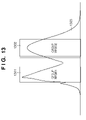
In step S1204, the grouping unit 103 groups the wafers in the lot in accordance with the correction value distribution (in other words, the characteristic distribution) by referring to the correction values for the wafers in the lot managed by the managing unit 101, and determines the reference wafer in each group. For example, if the correction value characteristics are bipolarized, as illustrated in a characteristic distribution shown in FIG. 13, groups WFG001 1301 and WFG002 1302 are determined, and a wafer having a most typical characteristic in these groups is determined as a reference wafer. Wafers other than the reference wafer are non-reference wafers, so the non-reference wafers are determined upon determining the reference wafer.
In the example shown in FIG. 14, group WFG001 includes wafer WF002 as a reference wafer, and wafers WF001 and WF004 as non-reference wafers, and group WFG002 includes wafer WF003 as a reference wafer, and wafer WF005 as a non-reference wafer. The grouping unit 103 registers “OUT” in the managing unit 101 as the group ID of a wafer omitted from the grouping based on the analysis result of the correction value distribution (characteristic distribution), and registers “MASTER” in the managing unit 101 as the wafer type of that wafer.
In step S1205, a sorting unit 106 changes the sorting order of the wafers from a sorting order before change 1501 to a sorting order after change 1502 for each group so that the wafers in the same group are arranged in sequence and the reference wafer comes first in the same group, as shown in FIG. 15. A method which sorts the wafers by the sorting unit 106 will be described herein, and a method which does not sort the wafers will be described later.
The next exposure process is performed for each group. In step S1206, it is checked whether the wafer to be processed is a reference wafer. If YES in step S1206, the process advances to step S1207. If NO in step S1206, the process advances to step S1208.
If the wafer to be processed is a reference wafer, in step S1207 the measurement unit 104 measures a first number of measurement points on the reference wafer, and the correction value determining unit 105 determines a correction value for the reference wafer based on the measurement result. The managing unit 101 registers the correction value, and the exposure unit 107 exposes the reference wafer to radiant energy while positioning it based on the correction value.
If the wafer to be processed is a non-reference wafer, in step S1208 the measurement unit 104 measures a second number (second number<first number) of measurement points on the non-reference wafer. The correction value determining unit 105 determines a correction value for the non-reference wafer based on the measurement result. The correction value determining unit 105 determines a correction value for the non-reference wafer using the correction value for a reference wafer (in other words, an immediately preceding reference wafer) belonging to the same group as the non-reference wafer, and the exposure unit 107 exposes the non-reference wafer to radiant energy.
Note that the wafer type of wafer WF006 omitted from groups WFG001 and WFG002 as the analysis result is a reference wafer. Therefore, the measurement unit 104 measures a first number of measurement points on wafer WF006, and the correction value determining unit 105 determines a correction value for the reference wafer based on the measurement result. The managing unit 101 registers the correction value, and the exposure unit 107 exposes the reference wafer to radiant energy while positioning it based on the correction value.
In the above-mentioned example, an exposure process is performed after sorting the wafers for each group by the sorting unit 106 in step S1205. Differently from this example, a correction value for the reference wafer in a group including a non-reference wafer to be processed may be retrieved from the table registered in the managing unit 101, and a correction value for the reference wafer may be referred to, as has been explained in the first embodiment.
As described above, according to this embodiment, the grouping accuracy can be changed because the wafers are grouped based on the analysis result of the correction values. This makes it possible to improve the precision of a correction value by, for example, narrowing the distribution range in each group, and to improve the throughput in an exposure process by, for example, widening the distribution range in each group.
Application Example
A device manufacturing method using the above-described exposure apparatus will be explained next. Devices (for example, a semiconductor integrated circuit device and liquid crystal display device) are manufactured by a step of exposing a substrate (for example, a wafer or glass plate) coated with a photosensitive agent to radiant energy using the exposure apparatus according to any of the above-described embodiments, a step of developing the substrate exposed in the exposing step, and other known steps.
While the present invention has been described with reference to exemplary embodiments, it is to be understood that the invention is not limited to the disclosed exemplary embodiments. The scope of the following claims is to be accorded the broadest interpretation so as to encompass all such modifications and equivalent structures and functions.
This application claims the benefit of Japanese Patent Application No. 2008-054065, filed Mar. 4, 2008, which is hereby incorporated by reference herein in its entirety.

Claims (7)

1. An exposure apparatus which exposes a substrate to radiant energy, the apparatus comprising:
a grouping unit configured to divide a plurality of substrates into a plurality of groups based on measurements of the plurality of substrates, and determine a reference substrate and a non-reference substrate for each of the plurality of groups;
a measurement unit configured to measure a first number of measurement points for the reference substrate, and measure a second number of measurement points for the non-reference substrate, the second number being smaller than the first number;
a correction value determining unit configured to determine a first correction value to position the reference substrate, and a second correction value to position the non-reference substrate; and
an exposure unit configured to expose the reference substrate to radiant energy by positioning the reference substrate based on the first correction value, and expose the non-reference substrate to radiant energy by positioning the non-reference substrate based on the second correction value,
wherein the correction value determining unit is configured to determine the first correction value for each of the plurality of groups based on measurement for the reference substrate performed by the measurement unit, and determines the second correction value for each of the plurality of groups based on measurement for the non-reference substrate performed by the measurement unit, and one of the measurement for the reference substrate performed by the measurement unit and the first correction value.
2. An apparatus according to claim 1, wherein the grouping unit is configured to divide the plurality of substrates into the plurality of groups based on a characteristic distribution of the plurality of substrates, which is obtained based on the measurements of the plurality of substrates.
3. An apparatus according to claim 1, further comprising a sorting unit configured to sort the plurality of substrates so that the substrates are arranged in sequence and the reference substrate is at a head of the sequence with respect to each of the plurality of groups,
wherein the measurement unit, the correction value determining unit and the exposure unit are configured to perform respective processes for each of the plurality of substrates sorted by the sorting unit.
4. A method of manufacturing a device, the method comprising:
exposing a substrate to radiant energy using an exposure apparatus;
developing the exposed substrate; and
processing the developed substrate to manufacture the device,
wherein the exposure apparatus is configured to expose a substrate to radiant energy, and the comprises:
a grouping unit configured to divide a plurality of substrates into a plurality of groups based on measurements of the plurality of substrates, and determine a reference substrate and a non-reference substrate for each of the plurality of groups;
a measurement unit configured to measure a first number of measurement points for the reference substrate, and measure a second number of measurement points for the non-reference substrate, the second number being smaller than the first number;
a correction value determining unit configured to determine a first correction value to position the reference substrate, and a second correction value to position the non-reference substrate; and
an exposure unit configured to expose the reference substrate to radiant energy by positioning the reference substrate based on the first correction value, and expose the non-reference substrate to radiant energy by positioning the non-reference substrate based on the second correction value,
wherein the correction value determining unit is configured to determine the first correction value for each of the plurality of groups based on measurement for the reference substrate performed by the measurement unit, and determines the second correction value for each of the plurality of groups based on measurement for the non-reference substrate performed by the measurement unit, and one of the measurement for the reference substrate performed by the measurement unit and the first correction value.
5. An exposure apparatus which includes a measurement unit, measures a first number of measurement points for a reference substrate by the measurement unit, measures a second number of measurement points for a non-reference substrate by the measurement unit, the second number being smaller than the first number, determines a first correction value to position the reference substrate, based on measurement for the reference substrate performed by the measurement unit, determines a second correction value to position the non-reference substrate, based on measurement for the non-reference substrate performed by the measurement unit and one of the measurement for the reference substrate performed by the measurement unit and the first correction value, exposes the reference substrate to radiant energy by positioning the reference substrate based on the first correction value, and exposes the non-reference substrate to radiant energy by positioning the non-reference substrate based on the second correction value, the apparatus comprising
a processor configured to divide a plurality of substrates into a plurality of groups based on measurements of the plurality of substrates, and determine the reference substrate and the non-reference substrate for each of the plurality of groups.
6. A method of manufacturing a device, the method comprising:
exposing a substrate to radiant energy using an exposure apparatus;
developing the exposed substrate; and
processing the developed substrate to manufacture the device,
wherein the exposure apparatus includes a measurement unit, measures a first number of measurement points for a reference wafer by the measurement unit, measures a second number of measurement points for a non-reference substrate by the measurement unit, the second number being smaller than the first number, determines a first correction value to position the reference substrate, based on measurement for the reference substrate performed by the measurement unit, determines a second correction value to position the non-reference substrate, based on measurement for the non-reference substrate performed by the measurement unit and one of the measurement for the reference substrate performed by the measurement unit and the first correction value, exposes the reference substrate to radiant energy by positioning the reference substrate based on the first correction value, and exposes the non-reference substrate to radiant energy by positioning the non-reference substrate based on the second correction value, and comprises:
a processor configured to divide a plurality of substrates into a plurality of groups based on measurements of the plurality of substrates, and determine the reference substrate and the non-reference substrate for each of the plurality of groups.
7. An exposure method including
a first measurement step of measuring a first number of measurement points for a reference substrate,
a first determination step of determining a first correction value to position the reference substrate, based on measurement for the reference substrate performed in the first measurement step,
a first exposure step of exposing the reference substrate to radiant energy by positioning the reference substrate based on the first correction value,
a second measurement step of measuring a second number of measurement points for a non-reference substrate, the second number being smaller than the first number,
a second determination step of determining a second correction value to position the non-reference substrate, based on measurement for the non-reference substrate performed in the second measurement step, and one of the measurement for the reference substrate performed in the first measurement step and the first correction value, and
a second exposure step of exposing the non-reference substrate by positioning the non-reference substrate based on the second correction value,
the method comprising
a grouping step of dividing a plurality of substrates into a plurality of groups based on measurements of the plurality of substrates, and determining the reference substrate and the non-reference substrate for each of the plurality of groups.
US12/395,487 2008-03-04 2009-02-27 Exposure apparatus and device manufacturing method Expired - Fee Related US8248584B2 (en)

Priority Applications (1)

Application Number Priority Date Filing Date Title
US13/544,790 US20120274916A1 (en) 2008-03-04 2012-07-09 Exposure apparatus and device manufacturing method

Applications Claiming Priority (2)

Application Number Priority Date Filing Date Title
JP2008054065A JP5166916B2 (en) 2008-03-04 2008-03-04 Apparatus for superimposing patterns and device manufacturing method
JP2008-054065 2008-03-04

Related Child Applications (1)

Application Number Title Priority Date Filing Date
US13/544,790 Continuation US20120274916A1 (en) 2008-03-04 2012-07-09 Exposure apparatus and device manufacturing method

Publications (2)

Publication Number Publication Date
US20090225292A1 US20090225292A1 (en) 2009-09-10
US8248584B2 true US8248584B2 (en) 2012-08-21

Family

ID=41053255

Family Applications (2)

Application Number Title Priority Date Filing Date
US12/395,487 Expired - Fee Related US8248584B2 (en) 2008-03-04 2009-02-27 Exposure apparatus and device manufacturing method
US13/544,790 Abandoned US20120274916A1 (en) 2008-03-04 2012-07-09 Exposure apparatus and device manufacturing method

Family Applications After (1)

Application Number Title Priority Date Filing Date
US13/544,790 Abandoned US20120274916A1 (en) 2008-03-04 2012-07-09 Exposure apparatus and device manufacturing method

Country Status (4)

Country Link
US (2) US8248584B2 (en)
JP (1) JP5166916B2 (en)
KR (1) KR101014100B1 (en)
TW (1) TW200951614A (en)

Cited By (2)

* Cited by examiner, † Cited by third party
Publication number Priority date Publication date Assignee Title
US20120274916A1 (en) * 2008-03-04 2012-11-01 Canon Kabushiki Kaisha Exposure apparatus and device manufacturing method
US10754264B2 (en) * 2017-11-13 2020-08-25 Canon Kabushiki Kaisha Lithography apparatus, lithography method, decision method, storage medium, and article manufacturing method

Families Citing this family (3)

* Cited by examiner, † Cited by third party
Publication number Priority date Publication date Assignee Title
KR101651860B1 (en) * 2015-01-30 2016-08-29 최은국 Apparatus for calssifying substrate
WO2018105658A1 (en) * 2016-12-08 2018-06-14 株式会社ブイ・テクノロジー Proximity exposure apparatus and proximity exposure method
EP3396458A1 (en) * 2017-04-28 2018-10-31 ASML Netherlands B.V. Method and apparatus for optimization of lithographic process

Citations (10)

* Cited by examiner, † Cited by third party
Publication number Priority date Publication date Assignee Title
JPH0463417A (en) 1990-07-03 1992-02-28 Fujitsu Ltd Manufacture of semiconductor device
JPH1055949A (en) 1996-08-12 1998-02-24 Nikon Corp Positioning method
US6278957B1 (en) 1993-01-21 2001-08-21 Nikon Corporation Alignment method and apparatus therefor
US20010049589A1 (en) 1993-01-21 2001-12-06 Nikon Corporation Alignment method and apparatus therefor
JP2001345243A (en) 2000-05-31 2001-12-14 Nikon Corp Evaluation method, position detection method, exposure method, and device manufacturing method
US20020042664A1 (en) 2000-05-31 2002-04-11 Nikon Corporation Evaluation method, position detection method, exposure method and device manufacturing method, and exposure apparatus
JP2002222752A (en) 2001-01-26 2002-08-09 Hitachi Ltd Semiconductor device manufacturing method and system
JP3451607B2 (en) 1994-12-08 2003-09-29 株式会社ニコン Positioning method and apparatus, and exposure method and apparatus
JP2005148531A (en) 2003-11-18 2005-06-09 Adtec Engineeng Co Ltd Aligner for printed-circuit board corresponding to expansion and contraction thereof
US20080294282A1 (en) * 2007-05-24 2008-11-27 Applied Materials, Inc. Use of logical lots in semiconductor substrate processing

Family Cites Families (4)

* Cited by examiner, † Cited by third party
Publication number Priority date Publication date Assignee Title
JPH04273115A (en) * 1991-02-27 1992-09-29 Hitachi Ltd Lot organization method and device
KR20080003618A (en) * 2006-07-03 2008-01-08 삼성전자주식회사 Wafer alignment method of exposure apparatus and exposure system using same
US7808613B2 (en) * 2006-08-03 2010-10-05 Asml Netherlands B.V. Individual wafer history storage for overlay corrections
JP5166916B2 (en) * 2008-03-04 2013-03-21 キヤノン株式会社 Apparatus for superimposing patterns and device manufacturing method

Patent Citations (12)

* Cited by examiner, † Cited by third party
Publication number Priority date Publication date Assignee Title
JPH0463417A (en) 1990-07-03 1992-02-28 Fujitsu Ltd Manufacture of semiconductor device
US6278957B1 (en) 1993-01-21 2001-08-21 Nikon Corporation Alignment method and apparatus therefor
US20010049589A1 (en) 1993-01-21 2001-12-06 Nikon Corporation Alignment method and apparatus therefor
US6876946B2 (en) 1993-01-21 2005-04-05 Nikon Corporation Alignment method and apparatus therefor
JP3451607B2 (en) 1994-12-08 2003-09-29 株式会社ニコン Positioning method and apparatus, and exposure method and apparatus
JPH1055949A (en) 1996-08-12 1998-02-24 Nikon Corp Positioning method
JP2001345243A (en) 2000-05-31 2001-12-14 Nikon Corp Evaluation method, position detection method, exposure method, and device manufacturing method
US20020042664A1 (en) 2000-05-31 2002-04-11 Nikon Corporation Evaluation method, position detection method, exposure method and device manufacturing method, and exposure apparatus
US20040126004A1 (en) 2000-05-31 2004-07-01 Nikon Corporation Evaluation method, position detection method, exposure method and device manufacturing method, and exposure apparatus
JP2002222752A (en) 2001-01-26 2002-08-09 Hitachi Ltd Semiconductor device manufacturing method and system
JP2005148531A (en) 2003-11-18 2005-06-09 Adtec Engineeng Co Ltd Aligner for printed-circuit board corresponding to expansion and contraction thereof
US20080294282A1 (en) * 2007-05-24 2008-11-27 Applied Materials, Inc. Use of logical lots in semiconductor substrate processing

Cited By (2)

* Cited by examiner, † Cited by third party
Publication number Priority date Publication date Assignee Title
US20120274916A1 (en) * 2008-03-04 2012-11-01 Canon Kabushiki Kaisha Exposure apparatus and device manufacturing method
US10754264B2 (en) * 2017-11-13 2020-08-25 Canon Kabushiki Kaisha Lithography apparatus, lithography method, decision method, storage medium, and article manufacturing method

Also Published As

Publication number Publication date
US20120274916A1 (en) 2012-11-01
KR20090095510A (en) 2009-09-09
JP5166916B2 (en) 2013-03-21
JP2009212312A (en) 2009-09-17
US20090225292A1 (en) 2009-09-10
TW200951614A (en) 2009-12-16
KR101014100B1 (en) 2011-02-14

Similar Documents

Publication Publication Date Title
US8566756B2 (en) Processing condition determining method and apparatus, display method and apparatus, processing apparatus, measurement apparatus and exposure apparatus, substrate processing system, and program and information recording medium
US8804137B2 (en) Unique mark and method to determine critical dimension uniformity and registration of reticles combined with wafer overlay capability
US10310490B2 (en) Method and apparatus of evaluating a semiconductor manufacturing process
US10031429B2 (en) Method of obtaining position, exposure method, and method of manufacturing article
US8248584B2 (en) Exposure apparatus and device manufacturing method
US5674651A (en) Alignment method for use in an exposure system
CN110546575B (en) Device manufacturing method
JP3348918B2 (en) Alignment method, exposure method using the method, and device manufacturing method
TWI879078B (en) Correlation-based overlay key centering system and method thereof
KR100439472B1 (en) Method and apparatus for measuring of processing error and method and apparatus for measuring of overlay
JP2023053800A (en) Method for determining arrangement of a plurality of shot areas on substrate, exposure method, exposure device, article production method, program and information processing device
US20230035488A1 (en) Metrology method
US6309944B1 (en) Overlay matching method which eliminates alignment induced errors and optimizes lens matching
US20040257573A1 (en) Position detecting method
US7212286B2 (en) Aligning method, exposure method, exposure apparatus, and device manufacturing method
EP3396457A1 (en) Device manufacturing method
US20080309903A1 (en) Exposure apparatus, method of manufacturing device, method applied to exposure apparatus and computer-readable medium
US8212990B2 (en) Exposure apparatus, information processing apparatus, and method of manufacturing device
CN222281048U (en) Overlay measurement mark
CN105759563B (en) Photomask and method for detecting photomask or wafer contamination
US20060212245A1 (en) Real-time mathematical model for wafer spin defect detection and for misalignment analyses
EP3376290A1 (en) Metrology method and method of device manufacture
JP5042412B2 (en) Measurement data correction method and measurement processing apparatus
JPH06181169A (en) Aligner and fabrication of semiconductor device
US20060266833A1 (en) System, method and computer software product for inspecting charged particle responsive resist

Legal Events

Date Code Title Description
AS Assignment

Owner name: CANON KABUSHIKI KAISHA, JAPAN

Free format text: ASSIGNMENT OF ASSIGNORS INTEREST;ASSIGNORS:SHIROIWA, MASATARO;SUZUKAWA, HIROKI;REEL/FRAME:022431/0653;SIGNING DATES FROM 20090219 TO 20090220

Owner name: CANON KABUSHIKI KAISHA, JAPAN

Free format text: ASSIGNMENT OF ASSIGNORS INTEREST;ASSIGNORS:SHIROIWA, MASATARO;SUZUKAWA, HIROKI;SIGNING DATES FROM 20090219 TO 20090220;REEL/FRAME:022431/0653

STCF Information on status: patent grant

Free format text: PATENTED CASE

FEPP Fee payment procedure

Free format text: PAYOR NUMBER ASSIGNED (ORIGINAL EVENT CODE: ASPN); ENTITY STATUS OF PATENT OWNER: LARGE ENTITY

FPAY Fee payment

Year of fee payment: 4

FEPP Fee payment procedure

Free format text: MAINTENANCE FEE REMINDER MAILED (ORIGINAL EVENT CODE: REM.); ENTITY STATUS OF PATENT OWNER: LARGE ENTITY

LAPS Lapse for failure to pay maintenance fees

Free format text: PATENT EXPIRED FOR FAILURE TO PAY MAINTENANCE FEES (ORIGINAL EVENT CODE: EXP.); ENTITY STATUS OF PATENT OWNER: LARGE ENTITY

STCH Information on status: patent discontinuation

Free format text: PATENT EXPIRED DUE TO NONPAYMENT OF MAINTENANCE FEES UNDER 37 CFR 1.362

FP Lapsed due to failure to pay maintenance fee

Effective date: 20200821