US8245063B2 - Clock selection for a communications processor having a sleep mode - Google Patents
Clock selection for a communications processor having a sleep mode Download PDFInfo
- Publication number
- US8245063B2 US8245063B2 US12/144,853 US14485308A US8245063B2 US 8245063 B2 US8245063 B2 US 8245063B2 US 14485308 A US14485308 A US 14485308A US 8245063 B2 US8245063 B2 US 8245063B2
- Authority
- US
- United States
- Prior art keywords
- clk
- register
- doublet
- clock
- output
- Prior art date
- Legal status (The legal status is an assumption and is not a legal conclusion. Google has not performed a legal analysis and makes no representation as to the accuracy of the status listed.)
- Active, expires
Links
- 238000004891 communication Methods 0.000 title claims description 11
- 230000005540 biological transmission Effects 0.000 claims description 4
- 230000007704 transition Effects 0.000 abstract description 7
- 238000010586 diagram Methods 0.000 description 13
- 102100040862 Dual specificity protein kinase CLK1 Human genes 0.000 description 7
- 102100040844 Dual specificity protein kinase CLK2 Human genes 0.000 description 7
- 101000749294 Homo sapiens Dual specificity protein kinase CLK1 Proteins 0.000 description 7
- 101000749291 Homo sapiens Dual specificity protein kinase CLK2 Proteins 0.000 description 7
- 230000000694 effects Effects 0.000 description 4
- 238000012545 processing Methods 0.000 description 4
- 230000003466 anti-cipated effect Effects 0.000 description 3
- 239000000872 buffer Substances 0.000 description 3
- 230000006870 function Effects 0.000 description 3
- 238000000034 method Methods 0.000 description 3
- 230000000737 periodic effect Effects 0.000 description 3
- 230000002093 peripheral effect Effects 0.000 description 3
- 230000008569 process Effects 0.000 description 2
- 230000004044 response Effects 0.000 description 2
- 230000001360 synchronised effect Effects 0.000 description 2
- 230000003321 amplification Effects 0.000 description 1
- 230000003139 buffering effect Effects 0.000 description 1
- 230000008859 change Effects 0.000 description 1
- 238000006243 chemical reaction Methods 0.000 description 1
- 230000008878 coupling Effects 0.000 description 1
- 238000010168 coupling process Methods 0.000 description 1
- 238000005859 coupling reaction Methods 0.000 description 1
- 239000013078 crystal Substances 0.000 description 1
- 238000013461 design Methods 0.000 description 1
- 238000006073 displacement reaction Methods 0.000 description 1
- 230000007246 mechanism Effects 0.000 description 1
- 238000003199 nucleic acid amplification method Methods 0.000 description 1
- 230000006641 stabilisation Effects 0.000 description 1
- 238000011105 stabilization Methods 0.000 description 1
- 230000003068 static effect Effects 0.000 description 1
- 238000012546 transfer Methods 0.000 description 1
Images


Classifications
-
- G—PHYSICS
- G06—COMPUTING; CALCULATING OR COUNTING
- G06F—ELECTRIC DIGITAL DATA PROCESSING
- G06F1/00—Details not covered by groups G06F3/00 - G06F13/00 and G06F21/00
- G06F1/26—Power supply means, e.g. regulation thereof
- G06F1/32—Means for saving power
- G06F1/3203—Power management, i.e. event-based initiation of a power-saving mode
- G06F1/3234—Power saving characterised by the action undertaken
- G06F1/324—Power saving characterised by the action undertaken by lowering clock frequency
-
- Y—GENERAL TAGGING OF NEW TECHNOLOGICAL DEVELOPMENTS; GENERAL TAGGING OF CROSS-SECTIONAL TECHNOLOGIES SPANNING OVER SEVERAL SECTIONS OF THE IPC; TECHNICAL SUBJECTS COVERED BY FORMER USPC CROSS-REFERENCE ART COLLECTIONS [XRACs] AND DIGESTS
- Y02—TECHNOLOGIES OR APPLICATIONS FOR MITIGATION OR ADAPTATION AGAINST CLIMATE CHANGE
- Y02D—CLIMATE CHANGE MITIGATION TECHNOLOGIES IN INFORMATION AND COMMUNICATION TECHNOLOGIES [ICT], I.E. INFORMATION AND COMMUNICATION TECHNOLOGIES AIMING AT THE REDUCTION OF THEIR OWN ENERGY USE
- Y02D10/00—Energy efficient computing, e.g. low power processors, power management or thermal management
Definitions
- the present invention relates to clock selection for communications systems having a sleep mode.
- the invention is directed to wireless communications systems having an accurate network clock, a low speed clock for a sleep mode, and a host clock for an operational mode.
- FIG. 1A shows a prior art communications system, which includes a System on a Chip (SoC) 110 , typically comprising baseband processing for a wireless communications system, which is coupled to an RF Front End 112 which accepts signals from antenna 113 , and performs the sequential operations of RF amplification, mixing to baseband using a local oscillator, and conversion to digital sampled signals using an analog to digital converter (ADC), and delivering these signals to the SoC 110 over interface 111 .
- a transmit stream may be generated by SoC 110 , which is provided to RF front end 112 as a baseband digital signal, which the RF front end 112 converts to an analog signal using a digital to analog converter (DAC).
- SoC 110 System on a Chip
- ADC analog to digital converter
- the SoC 110 accepts a clock signal NET_CLK generated by an accurate network clock source 106 . Generating the baseband modulation signals requires a relatively accurate clock compared to the other operations of the SoC 110 , and a low frequency SLEEP_CLK is sourced by a sleep clock generator 104 .
- the SLEEP_CLK may be coupled to a power sequencer 114 such as for powering up the SOC 110 and RF front end 112 when periodic beacons are received.
- the SoC 110 may also receive a HOST_CLK from a host clock generator 108 , which is also coupled to an applications processor 102 through host interface 116 , which may be a synchronous interface according to a known standard such as Peripheral Component Interconnect (PCI as described in www.pcisig.com), Universal Serial Bus (USB as described in www.usb.org), Secure Digital IO (SDIO as described in www.sdcard.org), or any host interface known for interconnecting an applications processor to a communications system through an interface.
- PCI Peripheral Component Interconnect
- USB Universal Serial Bus
- SDIO Secure Digital IO
- power saving modes are related to the useful time the device may be operated on a single charge.
- One prior art power saving mode uses a power sequencer 114 , which powers down various components of the system, which is shown as separated into components related to transmitting and receiving wireless signals PD 2 such as associated with the baseband interface 111 of the SoC 110 . For example, if there is no anticipated activity on baseband interface 111 , PD 2 may be asserted, thereby putting RF front end 112 into a powerdown state when no transmit or receive activity is anticipated, and PD 1 may be asserted when there is no anticipated data across the host interface 116 .
- partial powerdown for power-consuming parts of a processing element is known as a “sleep mode”, and may involve operation at a lower clock rate, or partial or complete powerdown of the associated system.
- Crystal oscillators such as those used to generate the host clock 108 and network clock 106 tend to consume a large amount of power compared to low frequency sleep clock 104 , in part because the displacement currents generated by each clock transition in the oscillator as well as the circuitry the clock is delivered to are proportional to clock rate, such that for all other considerations being equal, a lowest rate clock tends to result in a lower power dissipation.
- the sleep clock 104 operates a wake-up timer within power sequencer 114 , such that the SoC 110 and RF front end 112 are powered up to receive periodically transmitted signals such as beacons, and any required transmit frames are sent during these intervals.
- the SoC 110 indicates to the application processor 102 that it is entering a sleep mode, and the applications processor 102 uses a wakeup protocol with sequencer 114 to bring the system out of sleep mode when making a request 103 .
- the application processor 102 will queue requests and assert a powerup request to sequencer 114 .
- the SOC 110 comes out of sleep mode and has clock signals available, it indicates to the application processor 102 through a handshake mechanism across interface 116 that the application processor 102 may start sending requests and other relevant events.
- FIG. 1B shows the timing associated with this prior art wake-up method.
- HOST_CLK 164 is in a shutdown state until Wakeup SoC is asserted 154 , where the HOST_CLK stabilizes during an initialization time, and at time 156 , the HOST_CLK is stabilized and the request is handled, with the network clock 170 applied thereafter 156 .
- host clock 164 enters a shutdown mode at time 158 .
- the network clock 170 may stay active after end of request handling at time 158 to time 160 to complete the processing of any transmit network traffic which is generated, and enters a sleep mode thereafter 160 .
- a first object of this invention is a clock switching circuit for providing a glitch-free transition from one clock source to another clock source at a different frequency.
- a second object of the invention is a first and second doublet register, the first doublet register input coupled to a select input through an OR gate, the OR gate having another input coupled to the second doublet register output, an AND gate having one input coupled to the select input and the other input coupled to the first doublet register output, the output of the AND gate coupled to the input of the second doublet register input, and a clock output generated by the output of a second OR gate having inputs coupled to the outputs of a second AND gate and a third AND gate, the second AND gate coupled to a first clock source and the inverted output of the first doublet register, and second AND gate coupled to a second clock source and the output of the second doublet register, the first doublet register being clocked by the falling edge of the first clock and the second doublet register being clocked by the falling edge of the second clock.
- a clock selection function accepts a first clock input, a second clock input, a clock select, and generates a selected clock output.
- a first and second doublet register is formed by two registers having a doublet input coupled to one register and a doublet output coupled to the other register output, with the remaining register output coupled to the remaining register input, both registers of the doublet clocked by the same clock input.
- the first doublet register input is coupled to the output of an OR gate, the OR gate having one input coupled to the select input, and the other OR gate input coupled to the second doublet output.
- the second doublet has an input coupled to the output of an AND gate, the AND gate having a first input coupled to the select input and the other input coupled to the output of the first doublet.
- the first doublet output is inverted and coupled to a second AND gate, with the other input of the second AND gate coupled to the first clock input.
- the second doublet output is coupled to an input of a third AND gate, with the third AND gate other input coupled to the second clock input.
- the outputs of the second AND gate and third AND gate our ORed together to form the clock output.
- a clock select state machine clocked by NET_CLK has a first input HCA formed from a doublet register clocked by NET_CLK and a second input NCO formed from a doublet register clocked by NET_CLK.
- the clock select state machine generates EN_HSTCLK output, which is ANDED with HST_CLK_AVAIL and fed to a first doublet register clocked by HOST_CLK to generate SEL_HSTCLK, which is ANDED with HOST_CLK and ORed with the ANDing of EN_NETCLK and NET_CLK.
- the state machine moves between an IDLE state where EN_NETCLK is enabled and EN_HSTCLK is not enabled, a SLEEP state where EN_NETCLK is not enabled and EN_HOSTCLK is enabled, and WAIT, where neither EN_NETCLK nor EN_HOSTCLK is enabled.
- the state transitions are IDLE to SLEEP when NCO is asserted, SLEEP to WAIT when NCO is not asserted, and WAIT to IDLE a programmable number of NET_CLK cycles after entering WAIT.
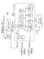
- FIG. 1A shows the block diagram for a prior art wireless system.
- FIG. 2A shows the block diagram for a wireless signal processor having a clock selection for sleep mode.
- FIG. 3 shows a schematic diagram for a clock switching circuit with two available clocks.
- FIG. 4 shows the timing diagram for the switching circuit of FIG. 3 .
- FIG. 6 shows the block diagram for an example clock selection for use in FIG. 5 .
- FIG. 7 shows a state diagram for a controller for FIG. 6 .
- FIG. 8 shows a timing diagram for the clock selector of FIG. 6 .
- FIG. 2A shows a wireless communications processor 200 including a wireless processor system on a chip (SOC) 208 coupled to an applications processor 202 which sends and receives data to the SOC 208 through a host interface 206 .
- the SOC 208 integrates all of the functions of the wireless system other than the front end components 234 described in FIG. 1A , including ADC, DAC, mixers, amplifiers, and other functions required to modulate and demodulate from antenna 236 to baseband digital interface 232 .
- the wireless processor 208 includes a host interface 216 to an internal bus 222 , which bus is also coupled to peripherals 218 , a DMA controller 220 , processor 228 , memory 230 , an interface 226 to the front end 234 , and a sleep state machine 224 .
- System on a chip wireless processor 208 accepts a network clock 212 which has higher accuracy than host clock 204 or sleep clock 214 .
- the sleep clock 214 is coupled to sleep state machine 224 , which may provide periodic wake-up signals to the processor 208 .
- Network clock 212 may be in a powerdown state, such as under control of the sleep state machine 224 , and during intervals when it is not important to transmit or receive wireless signals using the accurate but high power load network clock 212 , the wireless processor 208 may operate on host clock 212 , which is selected by selector 210 and delivered.
- the clock selector 210 is controlled by applications processor 208 such as through a request through the host interface 206 .
- the processor of FIG. 2A may operate in a sleep mode when there is no activity, or if there is no network activity, it can operate on HOST_CLK, and finally, when there is network traffic to receive or transmit, the wireless processor 208 can power the network clock and use this clock for wireless transmit and receive protocols.
- FIG. 2B shows the time sequence of operation of FIG. 2A for a host request which initiates a transmit operation.
- the wireless processor 208 runs on HOST_CLK from time 250 until the arrival of a host request at time 252 , whereupon the processor clock 262 is switched from HOST_CLK to NET_CLK for the duration of time required to handle the request to time 256 , after which the HOST_CLK is selected by 210 and provided to processor 204 .
- the clock selector 210 keeps the wireless processor 204 and associated circuits such as network clock 212 and front end components 234 in a low power state.
- the network clock 212 will be switched off and a sleep counter 224 coupled to sleep clock 214 will be maintained.
- the sleep counter 224 will wake up the SOC on a periodic basis to maintain existing network connections to remote stations coupled to antenna 236 .
- the wireless processor 208 will service this event by using HOST_CLK as CLK_OUT 238 .
- the wireless processor 208 can interrupt the sleep state machine and enable the network clock oscillator 212 . Once the network clock 212 oscillator has stabilized, the sleep state machine can instruct the clock select 210 to switch over to the network_clock 212 source and service the event.
- FIG. 3 shows one example embodiment for the clock selector 210 of FIG. 2A , suitable for the case where both HOST_CLK and NET_CLK provided to clock selector 210 are continuously present.
- the clock selector 300 accepts a first clock input CLK 1 and a second clock input CLK 2 , along with a SELECT input 302 .
- Registers 306 and 308 form a first doublet register 322 with an input coupled to first register 306 input, register 306 output coupled to register 308 input, and register 308 output forming the doublet register output.
- the first doublet register 322 is clocked with the negative edge of the first clock CLK 1 , shown with the convention for inversion as a inversion bubble at the clock input.
- Second doublet register 324 is similarly arranged, with first register 314 and second register 316 similarly configured with inverted clock for clocking the falling edge of second clock input CLK 2 .
- First doublet register 322 generates SEL_CLK 1 and second doublet register 324 generates SEL_CLK 2 , as will be described.
- OR gate 304 has one input coupled to the SEL select input 302 and the other input coupled to the second doublet 324 output SEL_CLK 1 .
- First AND gate 312 has one input coupled to SEL input 302 and the other input coupled to first doublet register output SEL_CLK 1 , with first AND gate output coupled to the input of second doublet register 322 .
- the first doublet register 322 output is also inverted and coupled to second AND gate 310 , with the remaining second AND gate input coupled to the first clock input.
- the second doublet register 324 output is coupled to an input of third AND gate 318 , which other AND gate input is coupled to the second clock input CLK 2 .
- Second OR gate 320 generates the selected clock output CLK_OUT 320 by performing an OR operation on the outputs of second AND gate 310 and third AND gate 318 .
- CLK 1 is shown at a slightly lower frequency than CLK 2 , however in a typical system the two frequencies may be any frequencies suitable for clocking static registers as shown.
- SEL waveform 354 When SEL waveform 354 is low, /SEL_CLK 1 356 and SEL_CLK 2 358 settle to LOW values, which cause gate 310 to enable first clock CLK 1 and disable second clock CLK 2 , thereby coupling CLK_OUT 320 to CLK 1 waveform 360 .
- SEL 354 is asserted
- /SEL_CLK 1 is asserted two negative CLK 1 edges later
- SEL_CLK 2 358 is asserted two clock edges after the assertion of /SEL_CLK 1 .
- no output clock is generated.
- CLK 2 Upon the assertion of SEL_CLK 2 358 , CLK 2 is coupled to CLK_OUT 360 , as shown during interval 366 .
- FIG. 5 shows a generalized clock selection 518 in the context of a wireless processor 506 where the HOST_CLK may not be available, as indicated by HST_CLK_AVAIL, and with a network clock NET_CLK, which is disabled by DIS_NETCLK and provided by sleep state machine 528 which generates NETCLK_OFF a stabilization time later, such that NETCLK_OFF is asserted to the state machine several cycles before and after DIS_NETCLK, such that a reliable and settled NET_CLK is available before and after NETCLK_OFF is asserted.
- Sleep clock 508 is a low frequency clock source which is continuously running and used by sleep state machine 528 to assert NETCLK_OFF during powerdown states, and to control powerup of the processor 506 during intervals such as beacons, when the wireless processor 506 needs to be ready to receive remote transmissions.
- the wireless processor 506 may include any other elements, including a bus 524 for interconnecting a processor 532 with memory 534 , interfaces 530 to the front end 512 , DMA controller 540 , peripherals 538 , and a host interface 536 to application processor 502 over an interface bus 504 , which may include a host processor request 516 indicating a pending request for wireless processor 506 response.
- the application processor 502 provides data for one or more packets to be transmitted, and the related packet data is accepted and queued in a buffer of host interface 536 , using the host clock 520 to buffer these packets.
- the buffering of packets to be transmitted by the wireless processor 506 allows the application processor to complete the transfer operation and continue with other operations.
- the SOC 506 may start a wakeup sequence whereby the network clock 508 is enabled and settles, after which the clock select 518 may switch to network clock for those parts of the system needing it.
- packets are transferred from the applications processor when the HOST_CLK is available and the NET_CLK is not available.
- packets have been queued from the applications processor 502 for transmission, and the HOST_CLK is turned off by the applications processor.
- the sleep state machine 528 requests the network clock NET_CLK 522 be taken out of disabled state such as by unasserting DIS_NETCLK, and the clock selection state machine 518 switches to NET_CLK when it is available, such as after HOST_CLK has been disabled.
- packets which were previously queued from the applications processor may be transmitted by the SOC 506 when the NET_CLK is available and the HOST_CLK is not available.
- FIG. 6 shows a block diagram for one embodiment of the clock selection 518 of FIG. 5 .
- a HOST_CLK 602 is provided, such as by the host processor interface, which interface includes an indicator HST_CLK_AVAIL, which enables the selection of HST_CLK only when this clock source is available.
- HST_CLK_AVAIL is generated by logic in the Host Interface 536 . It is unasserted at the end of a data transaction on the host bus 504 , anticipating the removal of the Host Clock, and is asserted again when a fresh transaction starts on the host interface and the HOST_CLK is again active.
- Clock selection 518 of FIG. 6 includes a first doublet register 632 clocked on the negative edge of HOST_CLK, the first doublet register 632 having an input coupled to the output of a first AND gate 606 , and the output of the first doublet register 632 generating SEL_HSTCLK and coupled to the input of a second AND gate 626 , the other input of which is coupled to HOST_CLK.
- a second doublet register input is coupled to HST_CLK_AVAIL, which is also coupled to an input of first AND gate 606 .
- Second doublet register 610 output generates HCA, which is coupled to a clock selection state machine, and generates EN_HSTCLK which is coupled to the other input of the first AND gate 606 .
- Third doublet register 614 input is coupled to NETCLK_OFF 612 , and third doublet register output generates NCO, which is also coupled to the input of the clock select state machine 622 .
- EN_NETCLK is generated by the clock select state machine, and is coupled to an input of third AND gate 624 , the other input of which is coupled to NETCLK 620 .
- An OR gate generates CLK_OUT from the output of the second AND gate and the output of the third AND gate.
- the clock select state machine, second doublet register, and third doublet register are clocked on the negative edge of NET_CLK.
- FIG. 7 One embodiment of a clock select state machine suitable for use in FIG. 6 622 is shown in FIG. 7 , where the state machine generates outputs EN_NETCLK and EN_HOSTCLK, which are preferably synchronous outputs generated from state bits of the state machine, as is known in the art of state machine design.
- FIG. 8 shows the timing diagram for the example embodiment described in FIGS. 6 and 7 .
- NET_CLK 802 is enabled by NETCLK_OFF such that the network clock oscillator runs for a longer time before and after NETCLK_OFF is unasserted.
- the HOST_CLK 804 is unavailable at time 830 , as indicated by HST_CLK_AVAIL, and does not return until time 834 .
- NET_CLK 804 is turned on at time 832 and off at time 836 .
- HCA is a doublet delay from Host Clock Available 806
- NCO is a doublet delay from NETCLK_OFF 808 .
- first doublet 632 is operative on HOST_CLK, which is not always present
- second doublet 610 , third doublet 614 , and clock select state machine 622 are operative on NET_CLK, which may similarly not be available during certain intervals, for which the state machine remains in a previous state until the NET_CLK becomes available again.
- NET_CLK It is generally desirable for the NET_CLK to be asserted before and after NETCLK_OFF sufficiently long enough for the state machine to reach state SLEEP, where HOST_CLK is generated. Additionally, it is desirable for HOST_CLK to be active for a sufficient time following HST_CLK_AVAIL for the state machine to reach state WAIT, where no clock is generated until NET_CLK is again active.
Abstract
Description
Claims (17)
Priority Applications (1)
| Application Number | Priority Date | Filing Date | Title |
|---|---|---|---|
| US12/144,853 US8245063B2 (en) | 2008-06-24 | 2008-06-24 | Clock selection for a communications processor having a sleep mode |
Applications Claiming Priority (1)
| Application Number | Priority Date | Filing Date | Title |
|---|---|---|---|
| US12/144,853 US8245063B2 (en) | 2008-06-24 | 2008-06-24 | Clock selection for a communications processor having a sleep mode |
Publications (2)
| Publication Number | Publication Date |
|---|---|
| US20090319817A1 US20090319817A1 (en) | 2009-12-24 |
| US8245063B2 true US8245063B2 (en) | 2012-08-14 |
Family
ID=41432490
Family Applications (1)
| Application Number | Title | Priority Date | Filing Date |
|---|---|---|---|
| US12/144,853 Active 2031-06-15 US8245063B2 (en) | 2008-06-24 | 2008-06-24 | Clock selection for a communications processor having a sleep mode |
Country Status (1)
| Country | Link |
|---|---|
| US (1) | US8245063B2 (en) |
Cited By (1)
| Publication number | Priority date | Publication date | Assignee | Title |
|---|---|---|---|---|
| US20140157023A1 (en) * | 2011-08-15 | 2014-06-05 | Panasonic Corporation | Network terminal, method for controlling the same, and network system |
Families Citing this family (4)
| Publication number | Priority date | Publication date | Assignee | Title |
|---|---|---|---|---|
| US9841804B2 (en) * | 2012-02-22 | 2017-12-12 | Silicon Laboratories Inc. | Clocking a processor |
| US9459886B2 (en) * | 2014-08-06 | 2016-10-04 | Texas Instruments Incorporated | Autonomous sleep mode |
| CN106934080B (en) * | 2015-12-29 | 2020-06-30 | 京微雅格(北京)科技有限公司 | Layout method of high-performance clock signal driving register |
| US11567527B2 (en) * | 2019-07-23 | 2023-01-31 | Texas Instruments Incorporated | Preemptive wakeup circuit for wakeup from low power modes |
Citations (1)
| Publication number | Priority date | Publication date | Assignee | Title |
|---|---|---|---|---|
| US6600345B1 (en) * | 2001-11-15 | 2003-07-29 | Analog Devices, Inc. | Glitch free clock select switch |
-
2008
- 2008-06-24 US US12/144,853 patent/US8245063B2/en active Active
Patent Citations (1)
| Publication number | Priority date | Publication date | Assignee | Title |
|---|---|---|---|---|
| US6600345B1 (en) * | 2001-11-15 | 2003-07-29 | Analog Devices, Inc. | Glitch free clock select switch |
Cited By (2)
| Publication number | Priority date | Publication date | Assignee | Title |
|---|---|---|---|---|
| US20140157023A1 (en) * | 2011-08-15 | 2014-06-05 | Panasonic Corporation | Network terminal, method for controlling the same, and network system |
| US9261936B2 (en) * | 2011-08-15 | 2016-02-16 | Panasonic Intellectual Property Management Co., Ltd. | Network terminal, method for controlling the same, and network system |
Also Published As
| Publication number | Publication date |
|---|---|
| US20090319817A1 (en) | 2009-12-24 |
Similar Documents
| Publication | Publication Date | Title |
|---|---|---|
| US8008949B1 (en) | Clock selection for a communications processor having a sleep mode | |
| US6115823A (en) | System and method for task performance based dynamic distributed power management in a computer system and design method therefor | |
| TWI720005B (en) | Data processing system, data processing device, and method of operating a slave device | |
| US6915438B2 (en) | Distributed power management method for monitoring control/status signal of sub-modules to manage power of sub-modules by activating clock signal during operation of sub-modules | |
| US6064626A (en) | Peripheral buses for integrated circuit | |
| US10509455B2 (en) | Method and apparatus to control a link power state | |
| US20190227971A1 (en) | Architecture for consolidating multiple sources of low-bandwidth data over a serial bus | |
| US8245063B2 (en) | Clock selection for a communications processor having a sleep mode | |
| US20180285292A1 (en) | System and method of sending data via additional secondary data lines on a bus | |
| US20030154336A1 (en) | Dual access serial peripheral interface | |
| EP1472609B1 (en) | Low-power bus interface | |
| JPH11145897A (en) | Mobile radio telephone set | |
| US20040003311A1 (en) | Data communication method | |
| US20160109928A1 (en) | Integrated circuit and low power method of operation | |
| US7185212B2 (en) | Method for PCI express power management using a PCI PM mechanism in a computer system | |
| CN116868177A (en) | Method for controlling chip and integrated circuit system | |
| CN115639897B (en) | Real-time voltage control module | |
| US6424179B1 (en) | Logic unit and integrated circuit for clearing interrupts | |
| US7206883B2 (en) | Interruption control system and method | |
| US11907154B2 (en) | Latency and power efficient clock and data recovery in a high-speed one-wire bidirectional bus | |
| US20070083782A1 (en) | Power configuration scheme of computer | |
| WO2017112311A1 (en) | Method and apparatus to control number of cores to transition operational states | |
| US20230176995A1 (en) | Power-saving techniques in computing devices through communication bus control | |
| JPH03192410A (en) | Communication equipment |
Legal Events
| Date | Code | Title | Description |
|---|---|---|---|
| AS | Assignment |
Owner name: REDPINE SIGNALS, INC., CALIFORNIA Free format text: ASSIGNMENT OF ASSIGNORS INTEREST;ASSIGNOR:KALLAM, SUBBA REDDY;REEL/FRAME:021695/0022 Effective date: 20081006 |
|
| STCF | Information on status: patent grant |
Free format text: PATENTED CASE |
|
| FPAY | Fee payment |
Year of fee payment: 4 |
|
| AS | Assignment |
Owner name: REDPINE SIGNALS, INC., CALIFORNIA Free format text: CORRECTIVE ASSIGNMENT TO CORRECT THE ASSIGNEE'S NAME INSIDE THE ASSIGNMENT DOCUMENT PREVIOUSLY RECOREDDY;REEL/FRAME:047873/0283 DED AT REEL: 021695 FRAME: 0022. ASSIGNOR(S) HEREBY CONFIRMS THE ASSIGNMENT;ASSIGNOR:KALLAM, SUBBA R Effective date: 20081006 Owner name: REDPINE SIGNALS, INC., CALIFORNIA Free format text: CORRECTIVE ASSIGNMENT TO CORRECT THE ASSIGNEE'S NAME INSIDE THE ASSIGNMENT DOCUMENT PREVIOUSLY RECORDED AT REEL: 021695 FRAME: 0022. ASSIGNOR(S) HEREBY CONFIRMS THE ASSIGNMENT;ASSIGNOR:KALLAM, SUBBA REDDY;REEL/FRAME:047873/0283 Effective date: 20081006 |
|
| MAFP | Maintenance fee payment |
Free format text: PAYMENT OF MAINTENANCE FEE, 8TH YR, SMALL ENTITY (ORIGINAL EVENT CODE: M2552); ENTITY STATUS OF PATENT OWNER: SMALL ENTITY Year of fee payment: 8 |
|
| AS | Assignment |
Owner name: SILICON LABORATORIES INC., TEXAS Free format text: ASSIGNMENT OF ASSIGNORS INTEREST;ASSIGNOR:REDPINE SIGNALS, INC.;REEL/FRAME:052560/0299 Effective date: 20200428 |
|
| FEPP | Fee payment procedure |
Free format text: ENTITY STATUS SET TO UNDISCOUNTED (ORIGINAL EVENT CODE: BIG.); ENTITY STATUS OF PATENT OWNER: LARGE ENTITY |
|
| FEPP | Fee payment procedure |
Free format text: MAINTENANCE FEE REMINDER MAILED (ORIGINAL EVENT CODE: REM.); ENTITY STATUS OF PATENT OWNER: LARGE ENTITY |