US8242913B2 - RFID tag communication apparatus - Google Patents
RFID tag communication apparatus Download PDFInfo
- Publication number
- US8242913B2 US8242913B2 US12/454,664 US45466409A US8242913B2 US 8242913 B2 US8242913 B2 US 8242913B2 US 45466409 A US45466409 A US 45466409A US 8242913 B2 US8242913 B2 US 8242913B2
- Authority
- US
- United States
- Prior art keywords
- antenna
- frequency
- rfid tag
- installation surface
- metal
- Prior art date
- Legal status (The legal status is an assumption and is not a legal conclusion. Google has not performed a legal analysis and makes no representation as to the accuracy of the status listed.)
- Active, expires
Links
Images


Classifications
-
- G—PHYSICS
- G06—COMPUTING OR CALCULATING; COUNTING
- G06K—GRAPHICAL DATA READING; PRESENTATION OF DATA; RECORD CARRIERS; HANDLING RECORD CARRIERS
- G06K7/00—Methods or arrangements for sensing record carriers, e.g. for reading patterns
- G06K7/0008—General problems related to the reading of electronic memory record carriers, independent of its reading method, e.g. power transfer
-
- G—PHYSICS
- G06—COMPUTING OR CALCULATING; COUNTING
- G06K—GRAPHICAL DATA READING; PRESENTATION OF DATA; RECORD CARRIERS; HANDLING RECORD CARRIERS
- G06K7/00—Methods or arrangements for sensing record carriers, e.g. for reading patterns
- G06K7/10—Methods or arrangements for sensing record carriers, e.g. for reading patterns by electromagnetic radiation, e.g. optical sensing; by corpuscular radiation
- G06K7/10009—Methods or arrangements for sensing record carriers, e.g. for reading patterns by electromagnetic radiation, e.g. optical sensing; by corpuscular radiation sensing by radiation using wavelengths larger than 0.1 mm, e.g. radio-waves or microwaves
- G06K7/10316—Methods or arrangements for sensing record carriers, e.g. for reading patterns by electromagnetic radiation, e.g. optical sensing; by corpuscular radiation sensing by radiation using wavelengths larger than 0.1 mm, e.g. radio-waves or microwaves using at least one antenna particularly designed for interrogating the wireless record carriers
Definitions
- the present disclosure relates to an RFID tag capable of communicating with an external source, and an RFID tag communication apparatus capable of transmitting and receiving information by wireless communication.
- the inductance of the apparatus antenna of the RFID tag communication apparatus increases due to mutual induction with the tag antenna of the RFID tag.
- the resonance frequency of the apparatus antenna is therefore set to a low value in advance with the amount of this increase in mind.
- RFID tag communication apparatuses that perform communication with RFID tags in accordance with these applications.
- needs such as the need to install an RFID tag communication apparatus on an installation surface made of metal, such as a steel desk, PC rack, or metal rack or shelf, and use the installed apparatus in an office or the home continue to emerge.
- the resonance frequency of the apparatus antenna is affected by the metal and therefore fluctuates.
- the RFID tag communication apparatus is provided on a non-metal installation surface, there is no such effect and the resonance frequency does not fluctuate.
- some type of device is needed to set the proper resonance frequency of the apparatus antenna (to set the resonance frequency with the RFID tag communication apparatus established as a single unit not placed on a metal installation surface or a non-metal installation surface).
- An aspect of the present application for achieving the above-described object is an RFID tag communication apparatus comprising a housing constituting an equipment shell including a bottom surface fixed in contact with a predetermined installation surface; an antenna provided along the bottom surface at a distance h from the bottom surface that transmits and receives information by wireless communication with an RFID tag including an IC circuit part that stores information and a tag antenna that transmits and receives information; and a radio frequency circuit including a carrier wave transmitting device that generates a carrier wave of a frequency fc for supplying power to the RFID tag, that transmits and receives information with the RFID tag; the frequency fc and the distance h being set to satisfy the correlation as: fo ⁇ fc ⁇ fm under the conditions that fm is set for a resonance frequency of the antenna when the bottom surface is fixed in contact with the installation surface made of a metal, and fo is set for a resonance frequency of the antenna when the bottom surface is fixed in contact with the installation surface made of a non-metal or the bottom surface is separated from the installation surface resulting in
- a carrier wave generated by the carrier wave transmitting device of the radio frequency circuit is transmitted to an RFID tag by an antenna so as to supply power to the RFID tag and, as a result, transmit and receive information by wireless communication with the RFID tag.
- each antenna has a specific resonance frequency and, during the above-described wireless communication, the communication efficiency increases to the extent that the resonance frequency coincides with (is close to) the frequency of the aforementioned carrier wave. Further, in a case where the RFID tag communication apparatus is disposed on a metal installation surface, for example, and is thus positioned close to metal, the resonance frequency of the above-described antenna is affected by the communication interference from that metal, causing the value of the resonance frequency to fluctuate and increase in comparison to a case of no metal.
- the fluctuating range (the value by which the resonance frequency increases) at that time increases and decreases in accordance with the distance between the antenna and metal, resulting in the resonance frequency varying (increasing) to a more significant degree as the distance between the antenna and metal decreases.
- the distance from the bottom surface (in other words, the distance from the installation surface; hereinafter the same) is kept constant within a certain range by placing the antenna along the bottom surface, keeping in mind that the apparatus is used in a form where the bottom surface of the housing contacts the installation surface.
- the first aspect of the present disclosure separates the antenna from the bottom surface by a distance h, thereby suppressing to within a certain range the fluctuating range (the difference
- the frequency of the carrier wave fc of the carrier wave transmitting device is set within that limited range, that is, so that fo ⁇ fc ⁇ fm.
- the difference between the resonance frequency fo when the bottom surface is fixed to a non-metal installation surface (or separated from the installation surface) and the carrier wave frequency fc can be made relatively small, and the difference between the resonance frequency fm when the bottom surface is fixed to a metal installation surface and the carrier wave frequency fc can also be made relatively small.
- are set in mutual association.
- Such settings make it possible to establish the resonance frequency and the carrier wave frequency relatively close to each other regardless of whether the bottom surface is fixed to a non-metal installation surface (or separated from the installation surface) or fixed to a metal installation surface, thereby maintaining high communication efficiency.
- FIG. 1 is a planar view showing a reader according to an embodiment of the present disclosure.
- FIG. 2 is a planar view of the reader with the cover removed (a cable is not shown for simplicity's sake).
- FIG. 3 is a vertical cross-sectional view of the reader based on the cross-section III-III of FIG. 2 .
- FIG. 4 is a block view showing the functional configuration of the reader.
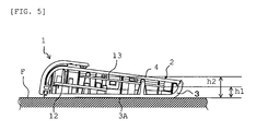
- FIG. 5 is a vertical cross-sectional view showing the reader in use.
- FIG. 6 is an equivalent circuit diagram of an antenna provided to the reader.
- FIG. 7 is a characteristics curve of frequency vs. gain of the antenna.
- the horizontal axis of FIG. 7 shows the resonance frequency of antenna, and the vertical axis of FIG. 7 shows the gain of the carrier wave emitted from the antenna.
- a reader 1 of the present embodiment comprises a compact housing 2 that constitutes an equipment shell, and is designed to be used when installed (fixed) to a suitable installation surface by a user (or when held by the user via the housing 2 while placed on an installation surface).
- An opening 5 for pulling the cable 6 used for power supply and signal transmission and reception into the housing 2 is provided on the front part (the upper side in FIG. 1 and FIG. 2 ) of the housing 2 .
- the housing 2 comprising a lower case 3 of a thin rectangular dish-like shape having a front end side that is open in the width direction, and the lid 4 of a flat rectangular shape that is installed on top of this lower case 3 .
- the lower case 3 comprises a bottom surface 3 A that comes in contact with the above-described installation surface when the reader 1 is placed on the installation surface, and inclines, in this example, in a direction in which the rear end side ascends toward the lid 4 .
- a flange part 4 a that curves downward and covers the opening of the front end of the lower case 3 is formed on the front end of the lid 4 .
- the opening 5 through which the cable 6 is pulled into the housing 2 is provided on the right side in the width direction of the lower part of the flange part 4 a (refer to FIG. 1 ).
- An installation part 4 b for mounting a clip 7 inserted through the flange part 4 a of the lid 4 is provided at the center of the width direction on the inside of the opening of the front end of the lower case 3 .
- the clip 7 comprises a bent shape that follows the flange part 4 a , and is mounted to the installation part 4 b so as to extend to the upper surface part of the lid 4 .
- the clip 7 can also be installed upside down so as to be positioned on the lower surface side of the lower case 3 (not shown).
- a cylinder-shaped first boss part 8 a , second boss part 8 b , and third boss part 8 c for screwing in the lid 3 are respectively provided in the corner areas, excluding the front left side corner area, of the lower case 3 , that is, in the front right side corner area, rear right side corner area, and rear left side corner area.
- the lid 4 covers the lower case 3 , overlapping the boss parts of the lid 4 corresponding to the boss parts 8 a to 8 c of the lower case 3 , and is installed to the lower case 3 by inserting screws (not shown) from the lower surface of the lower case 3 through through-holes 9 provided in the boss parts 8 a to 8 c of the lower case 3 and screwing the inserted screws into screw holes provided in the boss parts of the lid 4 .
- the control board 12 is a square-shaped electronic circuit board on which electronic circuits such as a radio frequency circuit 131 (refer to FIG. 4 described later) are mounted.
- This control board 12 is installed parallel to the upper surface part of the lid 4 , at a position near the bottom part of the lower case 3 , and extends from the location where the lower case 3 contacts the installation part 4 b to near the center part of the lower case 3 .
- the control board 12 in this example, is disposed toward a left wall part 3 b on the left side (the right side in FIG. 1 and FIG.
- the antenna 13 is a rectangular sheet body provided so that an antenna conductor 13 a forms a square-shaped loop coil, and is installed parallel to the control board 12 at a position higher than the control board 12 (refer to FIG. 3 ).
- the antenna 13 has a positional relationship such that it follows along the bottom surface 3 A of the lower case 3 (in this example, at somewhat of an incline), and the distance h to the bottom surface 3 A is within a predetermined range (h 1 ⁇ h ⁇ h 2 ; refer to FIG. 5 described later).
- the antenna 13 is disposed from above the center part of the control board 12 to a position of contact with the second boss part 8 b and the third boss part 8 c near a rear wall part 3 c of the lower case 3 .
- a pair of guide projections 16 positioned at the opening 5 on the lower right side of the flange part 4 a of the lid 4 is provided on the right side of the front end of the lower case 3 (refer to FIG. 2 ).
- the cable 6 connected to an external electrical device 130 (refer to FIG. 4 described later), such as a PC, is pulled between the guide projections 16 and into the housing 2 .
- the cable 6 is laid so as to hug the bottom part of the lower case 3 , following along the right side part and rear side part of the control board 12 , and is connected to the control board 12 via a connector 15 provided at the tip of the cable 6 (refer to FIG. 4 described later) and a board-side connector 135 provided at a position on the left side of the rear side part of the control board 12 (refer to FIG. 4 described later).
- the reader 1 comprises the control board 12 and the antenna 13 configured to transmit and receive information by wireless communication with an RFID circuit element To [included in an RFID tag (not shown) comprising an RFID label and RFID tag card, for example], which is the communication target, in the housing 2 .
- the control board 12 comprises the radio frequency circuit 131 configured to access an IC circuit part 150 by wireless communication via a tag antenna 151 of the RFID circuit element To and to process a signal read from that RFID circuit element To, a control circuit 133 configured to control the reader 1 in general including the radio frequency circuit 131 , a memory 134 configured to store information, and the board-side connecter 135 .
- the radio frequency circuit 131 includes a carrier wave generating part 132 configured to generate a carrier wave of a frequency fc for supplying power to the RFID circuit element To. Furthermore, the other end of the cable 6 is connected to the PC 130 in this example, and the reader 1 is supplied with power from the PC 130 via the cable 6 .
- the reader 1 is mainly used with the bottom surface 3 A of the lower case 3 of the housing 2 in contact with the top of an installation surface F and fixed to the installation surface F.
- high communication efficiency can be maintained during wireless communication with the RFID circuit element To, regardless of whether the installation surface F in contact with the bottom surface of the housing 2 is made of a metal or a non-metal.
- the antenna 13 is shown in a form where the antenna coil 13 a (inductance value L) connected between power supply terminals 18 and 18 from the control board is connected in series with a resistor 13 b (resistance value R) for line loss and a capacitor 13 c (capacitance C) for resonance.
- the antenna 13 has a specific resonance frequency that is determined by the inductance L of the antenna coil 13 a and the capacitance C of the capacitor 13 c.
- the communication efficiency increases to the extent the resonance frequency f of this antenna 13 and the aforementioned frequency fc of the carrier wave coincide (are close to each other).
- the resonance frequency f of the antenna is affected by the communication interference caused by that metal, causing the value of the resonance frequency f to fluctuate and (in comparison to a case of no metal) increase.
- the fluctuating range (the value by which the resonance frequency f increases) at that time increases and decreases in accordance with the distance between the antenna 13 and the metal installation surface F, causing the resonance frequency f to vary (increase) to a more significant degree as the distance between the antenna 13 and the installation surface F decreases.
- the separated distance h from the bottom surface 3 A of the antenna 13 (in other words, the distance from the installation surface F) is kept constant within a certain range (in this example, h 1 ⁇ h ⁇ h 2 ), keeping in mind that the reader 1 is used in a form where the bottom surface 3 A contacts the installation surface F.
- between the resonance frequency fo when the reader 1 is fixed to a non-metal installation surface F (or sufficiently separated from the installation surface F) and the resonance frequency fm when the reader 1 is fixed to a metal installation surface F is kept within a certain range.
- the frequency fc of the carrier wave generated by the radio frequency circuit 132 and emitted from the antenna 13 is set within the range fo ⁇ fc ⁇ fm, in accordance with the setting of such a separated distance h of the antenna 13 .
- a curve k 1 indicated by the dashed line shows the characteristics of the resonance frequency fm of the antenna 13 when the bottom surface 3 A of the reader 1 is fixed in contact with the installation surface F made of metal (hereinafter, suitably expressed as “when the reader 1 is fixed to a metal installation surface”).
- the difference between the resonance frequency fo of the antenna 13 when the reader 1 is fixed to a non-metal installation surface and the resonance frequency fm of the antenna 13 when the reader 1 is fixed to a metal installation surface is suppressed to within a limited range (in the above example, 0.55 [MHz]) and, in this state, the carrier wave frequency fc is set to a frequency between the resonance frequency fo and the resonance frequency fm.
- the difference between the resonance frequency fo when the reader 1 is fixed to the installation surface F of a non-metal (or sufficiently separated from the installation surface F) and the carrier wave frequency fc can be made relatively small (in the above example, 0.46 [MHz]), and the difference between the resonance frequency fm when the reader 1 is fixed to the installation surface F made of a metal and the carrier wave frequency fc can also be made relatively small (in the above example, 0.09 [MHz]).
- the installation surface F is made of a metal or a non-metal, high communication efficiency can be reliably maintained.
- the minimum value h 1 of the separated distance h of the antenna 13 is set to 8.5 [mm], making it possible to suppress the fluctuating range of the resonance frequencies fo to fm to within a minimum range, and the maximum value h 2 is set to 15.8 [mm], making it possible to prevent the reader 1 from becoming too large in size.
- the separated distance h of the antenna 13 and the carrier wave frequency fc are set in mutual association, resulting in a resonance frequency fm of 13.65 [MHz] when the reader 1 is fixed to a metal installation surface and a resonance frequency fo of 13.10 [MHz] when the reader 1 is fixed to a non-metal installation surface for a carrier wave frequency fc of 13.56 [MHz].
- the value of the carrier wave frequency fc is 13.375 [MHz]; refer to FIG. 7 .
- the separated distance h of the antenna 13 may be set in association with the carrier wave frequency fc so that the frequency of an intersection point P of the first characteristics line k 1 and the second characteristics line k 2 described above coincides with the carrier wave frequency fc.
- the value of the carrier wave frequency fc is 13.38 [MHz]; refer to FIG. 7 .
- the value of the antenna gain of the antenna 13 of the carrier wave frequency fc is the same when the reader 1 is fixed to a non-metal installation surface and when the reader 1 is fixed to a metal installation surface (the value becomes the same value X; refer to FIG. 7 ). That is, when such a value of the carrier wave frequency fc is set, the same antenna gain can be achieved whether the reader 1 is fixed to a non-metal installation surface F or a metal installation surface F. This makes it possible to stably maintain high communication efficiency.
Landscapes
- Engineering & Computer Science (AREA)
- Physics & Mathematics (AREA)
- Health & Medical Sciences (AREA)
- Toxicology (AREA)
- Artificial Intelligence (AREA)
- Computer Vision & Pattern Recognition (AREA)
- General Physics & Mathematics (AREA)
- Theoretical Computer Science (AREA)
- Computer Networks & Wireless Communication (AREA)
- Electromagnetism (AREA)
- General Health & Medical Sciences (AREA)
- Near-Field Transmission Systems (AREA)
Abstract
Description
f=½π√(LC)
Thus, the
Claims (3)
Applications Claiming Priority (2)
| Application Number | Priority Date | Filing Date | Title |
|---|---|---|---|
| JP2008-137404 | 2008-05-27 | ||
| JP2008137404A JP5146664B2 (en) | 2008-05-27 | 2008-05-27 | Wireless tag communication device |
Publications (2)
| Publication Number | Publication Date |
|---|---|
| US20090295547A1 US20090295547A1 (en) | 2009-12-03 |
| US8242913B2 true US8242913B2 (en) | 2012-08-14 |
Family
ID=40810103
Family Applications (1)
| Application Number | Title | Priority Date | Filing Date |
|---|---|---|---|
| US12/454,664 Active 2030-12-26 US8242913B2 (en) | 2008-05-27 | 2009-05-21 | RFID tag communication apparatus |
Country Status (4)
| Country | Link |
|---|---|
| US (1) | US8242913B2 (en) |
| EP (1) | EP2128788B1 (en) |
| JP (1) | JP5146664B2 (en) |
| CN (1) | CN101593283B (en) |
Families Citing this family (5)
| Publication number | Priority date | Publication date | Assignee | Title |
|---|---|---|---|---|
| CN102857270A (en) * | 2011-06-28 | 2013-01-02 | 英业达股份有限公司 | Electronic device and fixing structure thereof |
| JP6132266B2 (en) * | 2013-03-05 | 2017-05-24 | パナソニックIpマネジメント株式会社 | Non-contact power feeding device |
| CN106295444B (en) * | 2013-11-27 | 2020-05-22 | 苏州木兰电子科技有限公司 | Low-power anti-interference antenna activation source |
| CN207852935U (en) * | 2015-08-03 | 2018-09-11 | 株式会社村田制作所 | Antenna assembly and electronic equipment |
| US11206061B2 (en) * | 2019-12-06 | 2021-12-21 | Assa Abloy Ab | Dynamic frequency tuning for inductive coupling systems |
Citations (7)
| Publication number | Priority date | Publication date | Assignee | Title |
|---|---|---|---|---|
| JPH08263609A (en) | 1995-03-22 | 1996-10-11 | Otec Denshi Kk | Non-contact card reader |
| JP2000148932A (en) | 1998-11-13 | 2000-05-30 | Hitachi Ltd | Reader or / and writer device and IC card system using the same |
| US6377176B1 (en) * | 2000-06-13 | 2002-04-23 | Applied Wireless Identifications Group, Inc. | Metal compensated radio frequency identification reader |
| EP1560149A2 (en) | 2004-01-30 | 2005-08-03 | Sony Corporation | Portable type information processing terminal device |
| US20070139285A1 (en) | 2004-09-22 | 2007-06-21 | Matsushita Electric Industrial Co., Ltd. | Loop antenna unit and radio communication medium processor |
| WO2007116830A1 (en) | 2006-04-03 | 2007-10-18 | Aruze Corp. | Radio ic tag |
| US20080194200A1 (en) * | 2004-11-18 | 2008-08-14 | Innovision Research & Technology Plc | Wireless Communicators |
Family Cites Families (4)
| Publication number | Priority date | Publication date | Assignee | Title |
|---|---|---|---|---|
| JPH08263610A (en) * | 1995-03-22 | 1996-10-11 | Otec Denshi Kk | Non-contact card reader |
| JP4440570B2 (en) * | 2003-08-29 | 2010-03-24 | 大日本印刷株式会社 | Non-contact data carrier |
| KR100847351B1 (en) * | 2004-11-25 | 2008-07-21 | 주식회사 손텍 | Radio Frequency Identification Label |
| US7239243B2 (en) * | 2005-03-04 | 2007-07-03 | Printronix, Inc. | RFID tag imager |
-
2008
- 2008-05-27 JP JP2008137404A patent/JP5146664B2/en active Active
-
2009
- 2009-05-21 US US12/454,664 patent/US8242913B2/en active Active
- 2009-05-27 EP EP09161217.6A patent/EP2128788B1/en active Active
- 2009-05-27 CN CN2009101455785A patent/CN101593283B/en not_active Expired - Fee Related
Patent Citations (8)
| Publication number | Priority date | Publication date | Assignee | Title |
|---|---|---|---|---|
| JPH08263609A (en) | 1995-03-22 | 1996-10-11 | Otec Denshi Kk | Non-contact card reader |
| JP2000148932A (en) | 1998-11-13 | 2000-05-30 | Hitachi Ltd | Reader or / and writer device and IC card system using the same |
| US6377176B1 (en) * | 2000-06-13 | 2002-04-23 | Applied Wireless Identifications Group, Inc. | Metal compensated radio frequency identification reader |
| EP1560149A2 (en) | 2004-01-30 | 2005-08-03 | Sony Corporation | Portable type information processing terminal device |
| US20070139285A1 (en) | 2004-09-22 | 2007-06-21 | Matsushita Electric Industrial Co., Ltd. | Loop antenna unit and radio communication medium processor |
| US20080194200A1 (en) * | 2004-11-18 | 2008-08-14 | Innovision Research & Technology Plc | Wireless Communicators |
| WO2007116830A1 (en) | 2006-04-03 | 2007-10-18 | Aruze Corp. | Radio ic tag |
| US20090273474A1 (en) | 2006-04-03 | 2009-11-05 | Aruze Corp. | Radio ic tag |
Also Published As
| Publication number | Publication date |
|---|---|
| JP2009290251A (en) | 2009-12-10 |
| JP5146664B2 (en) | 2013-02-20 |
| EP2128788B1 (en) | 2015-01-14 |
| EP2128788A2 (en) | 2009-12-02 |
| US20090295547A1 (en) | 2009-12-03 |
| CN101593283A (en) | 2009-12-02 |
| EP2128788A3 (en) | 2011-06-29 |
| CN101593283B (en) | 2013-02-13 |
Similar Documents
| Publication | Publication Date | Title |
|---|---|---|
| CN108321495B (en) | Antenna assembly, antenna device and electronic equipment | |
| US8242913B2 (en) | RFID tag communication apparatus | |
| US6243045B1 (en) | Removal data storing medium having loop antenna | |
| CN102109884B (en) | Information processing apparatus | |
| US9627760B2 (en) | Antenna device and wireless communication apparatus | |
| EP2733686B1 (en) | Gateway system including communication module and method of driving the same | |
| EP2360779A2 (en) | Radio transmission system and electronic device | |
| WO2012122230A2 (en) | Set top box or server having snap-in heat sink and smart card reader | |
| KR20120103501A (en) | Power-receiving device, wireless power-feeding system including power-receiving device, and wireless communication system including power-receiving device | |
| US9484618B2 (en) | Antenna configuration for electronic devices | |
| US12431746B2 (en) | Antenna and electromagnetic shield disposed on a flexible circuit substrate | |
| US7249895B2 (en) | Optical transceiver with capacitive coupled signal ground with chassis ground | |
| US20180278092A1 (en) | Non-contact power transmission apparatus and power supply device | |
| US7432866B2 (en) | Antenna device with ion-implanted resonant pattern | |
| CN210776774U (en) | RFID electronic tag antenna | |
| KR102046549B1 (en) | A internal antenna of portable terminal processing transaction information and a portable terminal comprising it | |
| CN113381188A (en) | Antenna structure and communication terminal | |
| US20240039342A1 (en) | Wireless charging device with nfc function | |
| JP4413766B2 (en) | Electronic device casing and wireless communication module | |
| CN221885378U (en) | Antenna mounting structure of intelligent watch | |
| KR101609115B1 (en) | Antenna device | |
| KR101670895B1 (en) | Antenna device | |
| CN115276136A (en) | Housing, accommodating slot, electronic device and charging stand | |
| US20080299934A1 (en) | Communication module having a biomodulator | |
| JP2010056815A (en) | Radio tag communication system |
Legal Events
| Date | Code | Title | Description |
|---|---|---|---|
| AS | Assignment |
Owner name: BROTHER KOGYO KABUSHIKI KAISHA, JAPAN Free format text: ASSIGNMENT OF ASSIGNORS INTEREST;ASSIGNORS:TAKEDA, MICHIHIRO;NAKAMURA, MITSURU;FUKUI, TOMOYASU;REEL/FRAME:022767/0961 Effective date: 20090512 |
|
| STCF | Information on status: patent grant |
Free format text: PATENTED CASE |
|
| FPAY | Fee payment |
Year of fee payment: 4 |
|
| MAFP | Maintenance fee payment |
Free format text: PAYMENT OF MAINTENANCE FEE, 8TH YEAR, LARGE ENTITY (ORIGINAL EVENT CODE: M1552); ENTITY STATUS OF PATENT OWNER: LARGE ENTITY Year of fee payment: 8 |
|
| MAFP | Maintenance fee payment |
Free format text: PAYMENT OF MAINTENANCE FEE, 12TH YEAR, LARGE ENTITY (ORIGINAL EVENT CODE: M1553); ENTITY STATUS OF PATENT OWNER: LARGE ENTITY Year of fee payment: 12 |