US8185048B2 - Communication apparatus - Google Patents
Communication apparatus Download PDFInfo
- Publication number
- US8185048B2 US8185048B2 US12/576,198 US57619809A US8185048B2 US 8185048 B2 US8185048 B2 US 8185048B2 US 57619809 A US57619809 A US 57619809A US 8185048 B2 US8185048 B2 US 8185048B2
- Authority
- US
- United States
- Prior art keywords
- casing
- electrode
- filling member
- transmitter
- dielectric constant
- Prior art date
- Legal status (The legal status is an assumption and is not a legal conclusion. Google has not performed a legal analysis and makes no representation as to the accuracy of the status listed.)
- Expired - Fee Related, expires
Links
Images


Classifications
-
- H—ELECTRICITY
- H04—ELECTRIC COMMUNICATION TECHNIQUE
- H04B—TRANSMISSION
- H04B13/00—Transmission systems characterised by the medium used for transmission, not provided for in groups H04B3/00 - H04B11/00
- H04B13/005—Transmission systems in which the medium consists of the human body
-
- H—ELECTRICITY
- H04—ELECTRIC COMMUNICATION TECHNIQUE
- H04B—TRANSMISSION
- H04B13/00—Transmission systems characterised by the medium used for transmission, not provided for in groups H04B3/00 - H04B11/00
Definitions
- the present invention relates to a communication apparatus used in a communication system in which transmission and reception is performed through a transmission medium such as a human body.
- a transmitter supplies an electric field corresponding to a modulation signal obtained by modulating an information signal to a human body serving as a transmission medium
- a receiver detects the electric field transmitted through the human body and performs demodulation to obtain the original signal corresponding to the electric field.
- a signal is transmitted by capacitive coupling, instead of causing a through-current to flow to a transmission medium.
- the capacitive coupling between a transmission electrode and the transmission medium, the transmission electrode providing a capacitive coupling between the transmission medium and a transmission circuit of a transmitter, and the capacitive coupling between a reception electrode and the transmission medium, the reception electrode providing a capacitive coupling between the transmission medium and a reception circuit of a receiver be large.
- the transmitter or receiver described above is provided in the casing of an electronic apparatus such as a cellular phone, a space is formed between the internal surface of the casing and the transmission electrode of the transmitter or between the internal surface of the casing and the reception electrode of the receiver. Hence, the capacitive coupling between the transmission or reception electrode and a transmission medium is reduced, and a transmission signal thus becomes faint. Furthermore, due to a variation in the space between the internal surface of the casing and the transmission or reception electrode, the signal intensity varies.
- the present invention provides a communication apparatus including a transmitter or receiver for electric field communication and being capable of achieving reliable electric field communication.
- a communication apparatus includes a transmitter configured to supply an information signal as an electric field to a transmission medium; a receiver configured to detect the electric field through the transmission medium to acquire the information signal; an insulating casing that accommodates at least one of the transmitter and the receiver; and a filling member that is arranged at least one of between the casing and the transmitter and between the casing and the receiver.
- the filling member is formed of a material having a dielectric constant higher than a dielectric constant of the casing.
- At least one of the transmitter and the receiver accommodated in the casing includes an electrode arranged so as to face an internal surface of the casing with the filling member arranged therebetween.
- part of the internal surface of the casing includes a thin wall portion.
- At least one of the transmitter and the receiver accommodated in the casing includes an electrode arranged so as to face an internal surface of the casing with the filling member arranged therebetween.
- the filling member is filled in an opening formed in the casing.
- the transmitter is provided in the casing.
- a communication apparatus includes a transmitter configured to supply an information signal as an electric field to a transmission medium; a receiver configured to detect the electric field through the transmission medium to acquire the information signal; an insulating casing that accommodates at least one of the transmitter and the receiver; and a filling member that is arranged at least one of between the casing and the transmitter and between the casing and the receiver, reliable electric field communication can be achieved.
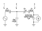
- FIG. 1A is an equivalent circuit diagram of a communication system using electric field communication in a case where a receiver is provided in a casing;
- FIG. 1B is an equivalent circuit diagram of the communication system using electric field communication in a case where a transmitter is provided in a casing;
- FIG. 2 is a graph showing changes in output voltage when the space between the internal surface of the casing and a transmission electrode of the transmitter and the space between the internal surface of the casing and a reception electrode of the receiver are changed;
- FIG. 3 illustrates an apparatus main body of a communication apparatus according to an embodiment of the present invention
- FIG. 4 is a cross-sectional view of the apparatus main body taken along line IV-IV of FIG. 3 ;
- FIGS. 5A to 5D are illustrations showing other examples of a communication apparatus according to an embodiment of the present invention.
- FIG. 6 is a characteristic diagram showing the relationship between the communication speed and the distance between an electrode and a human body.
- FIGS. 1A and 1B illustrate equivalent circuits of a communication system using electric field communication.
- FIG. 1A is an equivalent circuit diagram in a case where a receiver is provided in a casing.
- FIG. 1B is an equivalent circuit diagram in a case where a transmitter is provided in a casing.
- a capacitance Ct is formed between a transmitter 1 and a human body 2 serving as a transmission medium, and a capacitance Cr is formed between a receiver 3 and the human body 2 .
- a capacitance Chg is formed between the human body 2 and the ground, and a capacitance Cx, which is an unstable series capacitance, is formed between the internal surface of the casing and a transmission electrode of the transmitter or between the internal surface of the casing and a reception electrode of the receiver.
- the unstable series capacitance Cx is formed between the internal surface of the casing and the reception electrode of the receiver 3 , as shown in FIG. 1A .
- the reception electrode of the receiver 3 has an area of 4 square centimeters (2 cm ⁇ 2 cm) and the casing accommodating the receiver 3 is formed of an acrylonitrile butadiene styrene (ABS) resin having a relative dielectric constant of 3 and a thickness of about 0.3 mm
- ABS acrylonitrile butadiene styrene
- the capacitance Chg is assumed to be 110 pF (it is assumed that the feet are fixed to the ground) and the detected capacitance at the receiver 3 is 1 pF
- the unstable series capacitance Cx formed in a space of 1 mm or less between the internal surface of the casing and the reception electrode of the receiver 3 is 3 pF or more.
- the unstable series capacitance Cx is formed between the internal surface of the casing and the transmission electrode of the transmitter 1 , as shown in FIG. 1B .
- the transmission electrode of the transmitter 1 has an area of 4 square centimeters (2 cm ⁇ 2 cm) and the casing accommodating the transmitter 1 is formed of an ABS resin having a relative dielectric constant of 3 and a thickness of about 0.3 mm
- the capacitance Chg is assumed to be 110 pF (it is assumed that the feet are fixed to the ground) and the detected capacitance at the transmitter 1 is 1 pF
- the unstable series capacitance Cx formed in a space of 1 mm or less between the internal surface of the casing and the transmission electrode of the transmitter 1 is 3 pF or more.
- the inventors of the present invention have focused on the fact that in a case where a transmitter or a receiver for electric field communication is provided in an electronic apparatus, when a space (air-gap) is formed between a transmission electrode of the transmitter and the internal surface of the casing of the electronic apparatus or between a reception electrode of the receiver and the internal surface of the casing of the electronic apparatus, an unstable series capacitance is formed, which inhibits reliable electric field communication. Then, the inventors have found that by filling the air-gap formed between the transmission electrode or the reception electrode and the internal surface of the casing with a dielectric material, the unstable series capacitance can be eliminated and reliable electric field communication can thus be achieved, and have made the present invention based on the finding.
- the gist of the present invention is to achieve more reliable electric field communication using a communication apparatus including a transmitter configured to supply an information signal as an electric field to a transmission medium; a receiver configured to detect the electric field through the transmission medium to acquire the information signal; an insulating casing that accommodates at least one of the transmitter and the receiver; and a filling member that is arranged at least one of between the casing and the transmitter and between the casing and the receiver.
- FIG. 2 shows the result of the examination.
- the space greatly affects output voltage, and thus greatly affects communication.
- This system mainly includes a transmission medium, such as a human body, for transmitting an information signal through an electric field; a transmitter configured to supply the information signal as the electric field to the transmission medium; and a receiver configured to detect the electric field through the transmission medium and receive the electric field to acquire the information signal.
- a transmission medium such as a human body
- a transmitter configured to supply the information signal as the electric field to the transmission medium
- a receiver configured to detect the electric field through the transmission medium and receive the electric field to acquire the information signal.
- electrical capacitive coupling is formed through a capacitor between the transmitter and the transmission medium (for example, a human body) and a capacitor between the receiver and the transmission medium, and an information signal is converted into an electric field and then transmitted through the transmission medium.
- the transmission medium for example, a human body
- a displacement current flows to the transmission medium, it is not necessary to establish electric conduction of the transmission medium.
- the capacitive coupling between the transmitter and the transmission medium can be formed with a thin cloth located therebetween, transmission
- the transmitter temporarily modulates an information signal in a predetermined modulation method and supplies the modulated information signal as an electric field to the transmission medium.
- the transmitter includes a modulation circuit configured to modulate a carrier wave using the information signal; a conversion circuit configured to amplify the modulated signal and convert the amplified signal into a voltage change; and a transmission electrode configured to supply an electric field to the transmission medium.
- the receiver detects the electric field through the transmission medium to acquire the information signal.
- the receiver includes a reception electrode configured to receive an electric field from the transmission medium, the reception electrode facing the transmission medium; a detection circuit configured to amplify and detect the electric field; and a demodulation circuit configured to demodulate the modulated information signal by using the detected physical quantity.
- the transmitter modulates, using an information signal, a carrier wave having a frequency (within a range from several tens of kHz to several tens of MHz) at which the human body exhibits conductivity.
- the modulated information signal is amplified and then converted into a voltage change.
- an electric field corresponding to the modulated information signal is generated near the electrode.
- the electric field is applied to a human body.
- the electric field applied to the human body is received at the reception electrode of the receiver.
- the detection circuit detects the modulated information signal.
- the demodulation circuit which is provided downstream the detection circuit, performs demodulation using the carrier wave used in the transmitter to obtain the original information signal.
- transmission and reception of an information signal can be performed through a human body serving as a transmission medium.
- modulation methods such as amplitude modulation (AM), frequency modulation (FM), amplitude-shift keying (ASK), phase-shift keying (PSK), and quadrature shift keying (QSK), may be used as the modulation method described above.
- a communication apparatus has a configuration in which a transmitter or a receiver for a system in which the electric field communication described above is performed is provided in the casing of an apparatus main body 11 shown in FIG. 3 .
- the apparatus main body 11 includes a display 12 and an operation buttons 13 .
- FIG. 4 is a cross-sectional view of the apparatus main body 11 taken along line IV-IV of FIG. 3 .
- a transmitter is provided in an insulating casing 21 .
- the transmitter mainly includes a transmission electrode 22 and circuit boards 23 .
- the transmission electrode 22 is provided on the internal surface of the casing 21 with a filling member 24 arranged therebetween.
- the circuit boards 23 are provided on the transmission electrode 22 with spacers 25 arranged therebetween.
- the transmission electrode 22 is electrically connected to the circuit boards 23 .
- a space formed between the internal surface of the casing 21 and the transmission electrode 22 is filled with the filling member 24 , so that an unstable capacitance is prevented from being formed between the internal surface of the casing 21 and the transmission electrode 22 . Consequently, electric field loss between the internal surface of the casing 21 and the transmission electrode 22 can be reduced to as small as possible.
- the filling member 24 is placed between the internal surface of the casing 21 and the transmission electrode 22 , the electrostatic capacitance between the transmission electrode or the reception electrode and the transmission medium increases, thus reducing signal attenuation. Furthermore, since no air-gap is formed between the internal surface of the casing 21 and the transmission electrode 22 , a variation in the signal intensity caused by a variation in the capacitance of an air-gap can be reduced. Consequently, reliable electric field communication can be achieved.
- a high dielectric material having a relatively high dielectric constant be used as a material of the filling member 24 .
- adhesives such as an epoxy adhesive (a relative dielectric constant within a range from 2.5 to 6), an acrylic adhesive (a relative dielectric constant within a range from 2.7 to 4.5), a silicone adhesive (a relative dielectric constant within a range from 3.5 to 5), and a urethane adhesive (a relative dielectric constant within a range from 6.5 to 7.1); rubbers, such as a silicone rubber (a relative dielectric constant within a range from 3 to 3.5); resins, such as, an ABS resin (a relative dielectric constant within a range from 2.4 to 4.1) and a urethane resin (a relative dielectric constant within a range from 6.5 to 7.1); and the like may be used as high dielectric constant materials.
- the filling member 24 be formed of a material having a dielectric constant higher than the dielectric constant of the casing 21 .
- signal attenuation can be reduced and an excellent communication state can be achieved compared with a case where the internal surface of the casing 21 and the transmission electrode 22 are brought into close contact to each other without forming an air-gap therebetween.
- the casing 21 is formed of an ABS resin having a relative dielectric constant of 3
- a material having a relative dielectric constant of 4 or more is selected as a material of the filling member 24 .
- a conductive material having a relatively high conductivity may be used as a material of the filling member 24 .
- conductive adhesives such as an epoxy conductive adhesive and a polyimide conductive adhesive, a silver paste, and the like may be used as high-conductivity materials.
- FIGS. 5A to 5D are illustrations showing other examples of a communication apparatus according to an embodiment of the present invention.
- the transmission electrode 22 of the transmitter accommodated in the casing 21 faces the internal surface of the casing 21 and part of the internal surface of the casing 21 includes a thin wall portion 21 a .
- the filling member 24 is filled in an area including the thin wall portion 21 a . That is, the thin wall portion 21 a is provided on the internal surface of the casing 21 , and the transmission electrode 22 is provided on the internal surface of the casing 21 with the filling member 24 arranged therebetween in the area including the thin wall portion 21 a .
- the thin wall portion 21 a is provided in the area of the casing 21 that faces the transmission electrode 22 and the filling member 24 is filled in the thin wall portion 21 a , the volume ratio of the filling member 24 can be increased, thereby efficiently reducing signal attenuation.
- the transmission electrode 22 of the transmitter accommodated in the casing 21 faces the internal surface of the casing 21 and the internal surface includes an opening 21 b .
- the filling member 24 is filled in the opening 21 b , and the filling member 24 is exposed to the outside of the casing 21 . That is, the opening 21 b is provided in the casing 21 , and the transmission electrode 22 is provided on the internal surface of the casing 21 with the filling member 24 arranged therebetween in the opening 21 b .
- the opening 21 b is provided in the area of the casing 21 that faces the transmission electrode 22 and the filling member 24 is filled in the opening 21 b , the volume ratio of the filling member 24 can be increased, thereby efficiently reducing signal attenuation.
- the filling member 24 is filled in the opening 21 b , when a conductive material is used as a material of the filling member 24 , it is not necessary to cause the transmission electrode 22 and a human body serving as a transmission medium to be brought into conduction with each other.
- the filling member 24 formed of a conductive material may be covered with an insulating material 26 .
- Data communication was performed using electric field communication while a material arranged between a transmission electrode of a transmitter and a human body phantom (model) was changed, and a reduction in the communication speed according to the distance between the transmission electrode and the human body phantom was examined. In addition, a reduction in the communication speed according to the distance between a reception electrode of a receiver and the human body phantom was also examined.
- FIG. 6 shows the examination results. The communication speed was measured at a carrier frequency of 10 MHz and a signal amplitude of 1 Vp-p. For the ordinate of FIG. 6 , standardization was performed by setting the communication speed when the electrodes and the human body phantom were in close contact to each other to 100%.
- the communication speed recovered from 17% to 53% in the case of an air-gap of 0.05 mm, and recovered from 8% to 27% in the case of an air-gap of 0.1 mm.
- a urethane resin having a relative dielectric constant of 7 between the transmission electrode and the human body phantom the communication speed recovered from 17% to 100% in the case of an air-gap of 0.05 mm, and recovered from 8% to 62% in the case of an air-gap of 0.1 mm.
- the present invention is not limited to the embodiment described above and various changes can be made to the present invention.
- the present invention is not limited to this.
- the present invention can also be applied in a similar manner to the case where a receiver is provided in the casing of an apparatus main body.
- sizes, values, and the like set in the foregoing embodiment are not particularly limited. The sizes, values, and the like can be changed within the range of the present invention.
- various changes can be made to the present invention in an appropriate manner without departing from the scope of the present invention.
Abstract
Description
Claims (17)
Applications Claiming Priority (4)
| Application Number | Priority Date | Filing Date | Title |
|---|---|---|---|
| JP2007-111317 | 2007-04-20 | ||
| JP2007111317 | 2007-04-20 | ||
| PCT/JP2008/057520 WO2008130007A1 (en) | 2007-04-20 | 2008-04-17 | Communication device |
| JP2008-542120 | 2008-09-04 |
Related Parent Applications (1)
| Application Number | Title | Priority Date | Filing Date |
|---|---|---|---|
| PCT/JP2008/057520 Continuation WO2008130007A1 (en) | 2007-04-20 | 2008-04-17 | Communication device |
Publications (2)
| Publication Number | Publication Date |
|---|---|
| US20100029203A1 US20100029203A1 (en) | 2010-02-04 |
| US8185048B2 true US8185048B2 (en) | 2012-05-22 |
Family
ID=39875535
Family Applications (1)
| Application Number | Title | Priority Date | Filing Date |
|---|---|---|---|
| US12/576,198 Expired - Fee Related US8185048B2 (en) | 2007-04-20 | 2009-10-08 | Communication apparatus |
Country Status (5)
| Country | Link |
|---|---|
| US (1) | US8185048B2 (en) |
| JP (2) | JP4256468B2 (en) |
| KR (1) | KR20090128567A (en) |
| CN (1) | CN101663846B (en) |
| WO (1) | WO2008130007A1 (en) |
Cited By (1)
| Publication number | Priority date | Publication date | Assignee | Title |
|---|---|---|---|---|
| US20210359768A1 (en) * | 2020-05-13 | 2021-11-18 | Samsung Electronics Company, Ltd. | Efficient physical layer for intrabody communication networks |
Families Citing this family (12)
| Publication number | Priority date | Publication date | Assignee | Title |
|---|---|---|---|---|
| JP5273871B2 (en) * | 2007-02-14 | 2013-08-28 | カバ・アクチェンゲゼルシャフト | System and portable device for transmission of identification signals |
| DE102010010348A1 (en) * | 2010-03-05 | 2011-09-08 | Albert-Ludwigs-Universität Freiburg | Implantable device for detecting a vessel wall strain |
| JP2012064996A (en) * | 2010-09-14 | 2012-03-29 | Ntt Electornics Corp | Electric field communication device |
| US8457692B2 (en) | 2010-10-07 | 2013-06-04 | Research In Motion Limited | Method and system for preventing device operation when driving |
| CN102570127A (en) * | 2010-12-15 | 2012-07-11 | 富士康(昆山)电脑接插件有限公司 | Electric connector |
| US8611861B2 (en) | 2011-03-24 | 2013-12-17 | Blackberry Limited | Communications system including personal information token to store a personalized list and associated methods |
| WO2014148521A1 (en) * | 2013-03-21 | 2014-09-25 | 株式会社村田製作所 | Displacement sensor, pushing amount detection sensor, and touch input device |
| FR3007598B1 (en) * | 2013-06-24 | 2015-07-17 | Inside Secure | PORTABLE DEVICE COMPRISING MEANS FOR TRANSMITTING DATA BY INTRACORPORAL INDUCTIVE COUPLING AND CURRENT |
| FR3007599B1 (en) * | 2013-06-24 | 2016-11-11 | Inside Secure | PORTABLE DEVICE COMPRISING AN INTRACORPORAL CURRENT DATA TRANSMISSION ELECTRODE |
| WO2014207337A1 (en) * | 2013-06-24 | 2014-12-31 | Inside Secure | Portable device including means for transmitting data by inductive coupling and intracorporeal current |
| RU2577842C2 (en) * | 2014-06-11 | 2016-03-20 | Публичное акционерное Общество "Таганрогский авиационный научно-технический комплекс им. Г.М. Бериева" (ПАО "ТАНТК им. Г.М. Бериева") | Method of transmitting and receiving radio signals through eddy electric field and device therefor |
| MA56465A (en) * | 2019-07-01 | 2022-05-11 | Univ Hosei | ELECTRIC FIELD COMMUNICATION SYSTEM |
Citations (3)
| Publication number | Priority date | Publication date | Assignee | Title |
|---|---|---|---|---|
| JPH069220A (en) | 1991-01-18 | 1994-01-18 | Sumitomo Metal Mining Co Ltd | Stabilized or partially stabilized zirconia thin film and its production |
| US5914701A (en) | 1995-05-08 | 1999-06-22 | Massachusetts Institute Of Technology | Non-contact system for sensing and signalling by externally induced intra-body currents |
| WO2005002096A1 (en) | 2003-06-30 | 2005-01-06 | Nippon Telegraph And Telephone Corporation | Electric field-detecting optical device, tranceiver, positional information-acquiring system, and information input system |
Family Cites Families (2)
| Publication number | Priority date | Publication date | Assignee | Title |
|---|---|---|---|---|
| JPH069220U (en) * | 1992-07-07 | 1994-02-04 | 株式会社タイセー | Antenna device |
| JP4158097B2 (en) * | 2003-02-27 | 2008-10-01 | ソニー株式会社 | Authentication system |
-
2008
- 2008-04-17 CN CN2008800128629A patent/CN101663846B/en not_active Expired - Fee Related
- 2008-04-17 WO PCT/JP2008/057520 patent/WO2008130007A1/en active Application Filing
- 2008-04-17 JP JP2008542120A patent/JP4256468B2/en not_active Expired - Fee Related
- 2008-04-17 KR KR1020097023785A patent/KR20090128567A/en not_active Application Discontinuation
-
2009
- 2009-01-29 JP JP2009017914A patent/JP4469914B2/en not_active Expired - Fee Related
- 2009-10-08 US US12/576,198 patent/US8185048B2/en not_active Expired - Fee Related
Patent Citations (5)
| Publication number | Priority date | Publication date | Assignee | Title |
|---|---|---|---|---|
| JPH069220A (en) | 1991-01-18 | 1994-01-18 | Sumitomo Metal Mining Co Ltd | Stabilized or partially stabilized zirconia thin film and its production |
| US5914701A (en) | 1995-05-08 | 1999-06-22 | Massachusetts Institute Of Technology | Non-contact system for sensing and signalling by externally induced intra-body currents |
| JPH11509380A (en) | 1995-05-08 | 1999-08-17 | マサチューセッツ・インスティテュート・オブ・テクノロジー | Non-contact detection and signal system using human body as signal transmission medium |
| WO2005002096A1 (en) | 2003-06-30 | 2005-01-06 | Nippon Telegraph And Telephone Corporation | Electric field-detecting optical device, tranceiver, positional information-acquiring system, and information input system |
| US20050244166A1 (en) | 2003-06-30 | 2005-11-03 | Mitsuru Shinagawa | Electric field-detecting optical device, tranceiver, positional information-acquiring system, and information input system |
Non-Patent Citations (1)
| Title |
|---|
| Search Report dated May 20, 2008 from International Application No. PCT/JP2008/057250. |
Cited By (2)
| Publication number | Priority date | Publication date | Assignee | Title |
|---|---|---|---|---|
| US20210359768A1 (en) * | 2020-05-13 | 2021-11-18 | Samsung Electronics Company, Ltd. | Efficient physical layer for intrabody communication networks |
| US11700069B2 (en) * | 2020-05-13 | 2023-07-11 | Samsung Electronics Co., Ltd. | Efficient physical layer for intrabody communication networks |
Also Published As
| Publication number | Publication date |
|---|---|
| KR20090128567A (en) | 2009-12-15 |
| CN101663846A (en) | 2010-03-03 |
| JP2009118524A (en) | 2009-05-28 |
| WO2008130007A1 (en) | 2008-10-30 |
| US20100029203A1 (en) | 2010-02-04 |
| JP4469914B2 (en) | 2010-06-02 |
| JPWO2008130007A1 (en) | 2010-07-22 |
| CN101663846B (en) | 2013-09-25 |
| JP4256468B2 (en) | 2009-04-22 |
Similar Documents
| Publication | Publication Date | Title |
|---|---|---|
| US8185048B2 (en) | Communication apparatus | |
| US8150319B2 (en) | Communication apparatus | |
| JP4099484B2 (en) | Communications system. | |
| US6339385B1 (en) | Electronic communication devices, methods of forming electrical communication devices, and communication methods | |
| EP2139130A1 (en) | Communication system | |
| US8588684B2 (en) | Communication apparatus for performing data communication electrode unit and a living body | |
| US8175527B2 (en) | Portable apparatus | |
| US20080123599A1 (en) | Communication System, Communication Device And Method, And Program | |
| EP1117067A4 (en) | Ic card | |
| US11455478B2 (en) | Closed-system capacitive coupling RFID | |
| US8208852B2 (en) | Electronic apparatus for electric field communication | |
| KR20110040719A (en) | Transmitting/receiving apparatus and communications system with transmitting/receiving apparatus | |
| EP1398779A3 (en) | Dielectric reproducing apparatus, dielectric recording apparatus, and dielectric recording / reproducing apparatus | |
| JP4460546B2 (en) | Communication system, transmitter and receiver | |
| JP2008185537A (en) | Ac signal detection device, receiving device, and interboard transmission system | |
| CN211830848U (en) | Capacitance detection assembly and electronic equipment | |
| EP4318980A1 (en) | Power transmitter, power transmitting/receiving device, human-body communication device, and power transmitting/receiving system | |
| JP2010045570A (en) | Communication equipment | |
| CN110274629B (en) | Multifunctional integrated wireless sensor assembly and detection method | |
| CN205564958U (en) | Electronic equipment | |
| JP5340190B2 (en) | Communications system | |
| JP4460568B2 (en) | Receiver, transceiver, and control method | |
| JP5216565B2 (en) | Transmitter | |
| WO2004038847A2 (en) | Microwave circuit for use in a motion sensor | |
| JP2005323251A (en) | Modulation/demodulation circuit |
Legal Events
| Date | Code | Title | Description |
|---|---|---|---|
| AS | Assignment |
Owner name: ALPS ELECTRIC CO., LTD.,JAPAN Free format text: ASSIGNMENT OF ASSIGNORS INTEREST;ASSIGNORS:HEBIGUCHI, HIROYUKI;NAKASATO, MITSUHARU;SASAKI, MAKOTO;AND OTHERS;REEL/FRAME:023349/0653 Effective date: 20090930 Owner name: ALPS ELECTRIC CO., LTD., JAPAN Free format text: ASSIGNMENT OF ASSIGNORS INTEREST;ASSIGNORS:HEBIGUCHI, HIROYUKI;NAKASATO, MITSUHARU;SASAKI, MAKOTO;AND OTHERS;REEL/FRAME:023349/0653 Effective date: 20090930 |
|
| STCF | Information on status: patent grant |
Free format text: PATENTED CASE |
|
| FPAY | Fee payment |
Year of fee payment: 4 |
|
| FEPP | Fee payment procedure |
Free format text: PAYOR NUMBER ASSIGNED (ORIGINAL EVENT CODE: ASPN); ENTITY STATUS OF PATENT OWNER: LARGE ENTITY |
|
| AS | Assignment |
Owner name: ALPS ALPINE CO., LTD., JAPAN Free format text: CHANGE OF NAME;ASSIGNOR:ALPS ELECTRIC CO., LTD.;REEL/FRAME:048209/0318 Effective date: 20190101 |
|
| FEPP | Fee payment procedure |
Free format text: MAINTENANCE FEE REMINDER MAILED (ORIGINAL EVENT CODE: REM.); ENTITY STATUS OF PATENT OWNER: LARGE ENTITY |
|
| LAPS | Lapse for failure to pay maintenance fees |
Free format text: PATENT EXPIRED FOR FAILURE TO PAY MAINTENANCE FEES (ORIGINAL EVENT CODE: EXP.); ENTITY STATUS OF PATENT OWNER: LARGE ENTITY |
|
| STCH | Information on status: patent discontinuation |
Free format text: PATENT EXPIRED DUE TO NONPAYMENT OF MAINTENANCE FEES UNDER 37 CFR 1.362 |
|
| FP | Lapsed due to failure to pay maintenance fee |
Effective date: 20200522 |