US8158020B2 - Liquid crystal element, optical path deflecting element, and image displaying apparatus - Google Patents
Liquid crystal element, optical path deflecting element, and image displaying apparatus Download PDFInfo
- Publication number
- US8158020B2 US8158020B2 US11/913,378 US91337807A US8158020B2 US 8158020 B2 US8158020 B2 US 8158020B2 US 91337807 A US91337807 A US 91337807A US 8158020 B2 US8158020 B2 US 8158020B2
- Authority
- US
- United States
- Prior art keywords
- liquid crystal
- phase
- optical path
- formula
- compound
- Prior art date
- Legal status (The legal status is an assumption and is not a legal conclusion. Google has not performed a legal analysis and makes no representation as to the accuracy of the status listed.)
- Expired - Fee Related, expires
Links
- 0 CF.[1*]C1([N+]#[C-])CCC(CCCOCC)CC1.[1*]COC(=O)C1OC1[2*].[3*]COCC1COC([4*])([5*])O1 Chemical compound CF.[1*]C1([N+]#[C-])CCC(CCCOCC)CC1.[1*]COC(=O)C1OC1[2*].[3*]COCC1COC([4*])([5*])O1 0.000 description 22
- VYXHEFOZRVPJRK-UHFFFAOYSA-N CCOC(=O)C1OC1C Chemical compound CCOC(=O)C1OC1C VYXHEFOZRVPJRK-UHFFFAOYSA-N 0.000 description 4
- CDBLGGSCIQRZJA-UHFFFAOYSA-N CC1=CC=C(C)C=C1.CC1=CC=C(C)S1.CC1=CN=C(C)C=C1.CC1=CN=C(C)C=C1.CC1=CN=C(C)C=N1.CC1=CN=C(C)N=C1.CC1=CN=C(C)N=C1.CC1=CN=C(C)S1.CC1=CN=C(C)S1.CC1=NN=C(C)C=C1.CC1=NN=C(C)S1.CC1CCC(C)CC1.CC1COC(C)OC1.CC1COC(C)OC1.CC1CSC(C)SC1.CC1CSC(C)SC1.CN1CCN(C)CC1 Chemical compound CC1=CC=C(C)C=C1.CC1=CC=C(C)S1.CC1=CN=C(C)C=C1.CC1=CN=C(C)C=C1.CC1=CN=C(C)C=N1.CC1=CN=C(C)N=C1.CC1=CN=C(C)N=C1.CC1=CN=C(C)S1.CC1=CN=C(C)S1.CC1=NN=C(C)C=C1.CC1=NN=C(C)S1.CC1CCC(C)CC1.CC1COC(C)OC1.CC1COC(C)OC1.CC1CSC(C)SC1.CC1CSC(C)SC1.CN1CCN(C)CC1 CDBLGGSCIQRZJA-UHFFFAOYSA-N 0.000 description 3
- NYMDESIHRAWGIT-UHFFFAOYSA-N CC1=CC=C(C)C=C1.CC1=CN=C(C)C=C1.CC1=CN=C(C)C=C1.CC1=CN=C(C)N=C1.CC1=CN=C(C)N=C1.CC1=NN=C(C)C=C1.CC1CCC(C)CC1 Chemical compound CC1=CC=C(C)C=C1.CC1=CN=C(C)C=C1.CC1=CN=C(C)C=C1.CC1=CN=C(C)N=C1.CC1=CN=C(C)N=C1.CC1=NN=C(C)C=C1.CC1CCC(C)CC1 NYMDESIHRAWGIT-UHFFFAOYSA-N 0.000 description 3
- HPSRFJMDYFTALY-UHFFFAOYSA-N CCCCCCC1=CC=C(C2=CN=C(C3=CC=C(CCCCCC)C=C3)C=C2)C=C1 Chemical compound CCCCCCC1=CC=C(C2=CN=C(C3=CC=C(CCCCCC)C=C3)C=C2)C=C1 HPSRFJMDYFTALY-UHFFFAOYSA-N 0.000 description 3
- ATZLPEPWPJQANQ-UHFFFAOYSA-N CCCCCCCCC1=CN=C(C2=CC=C(OCCCCCC)C=C2)N=C1 Chemical compound CCCCCCCCC1=CN=C(C2=CC=C(OCCCCCC)C=C2)N=C1 ATZLPEPWPJQANQ-UHFFFAOYSA-N 0.000 description 3
- UFHCRJDBXDRRTE-UHFFFAOYSA-N CCCCCCCCCCCCC1=CN=C(C2=CC=C(C(=O)OC3=CC=C(F)C=C3)C=C2)N=C1 Chemical compound CCCCCCCCCCCCC1=CN=C(C2=CC=C(C(=O)OC3=CC=C(F)C=C3)C=C2)N=C1 UFHCRJDBXDRRTE-UHFFFAOYSA-N 0.000 description 3
- CZVGOAPQSLSDNN-UHFFFAOYSA-N CCCCCCCCCCOC1=CC=C(C2=NC=C(CCCCCCCC)C=N2)C=C1 Chemical compound CCCCCCCCCCOC1=CC=C(C2=NC=C(CCCCCCCC)C=N2)C=C1 CZVGOAPQSLSDNN-UHFFFAOYSA-N 0.000 description 3
- XYGUNTNTTDQAGL-UHFFFAOYSA-N CCCCCCCCCCOC1=CC=C(C2=NC=C(OCCCCCCCC)C=N2)C=C1 Chemical compound CCCCCCCCCCOC1=CC=C(C2=NC=C(OCCCCCCCC)C=N2)C=C1 XYGUNTNTTDQAGL-UHFFFAOYSA-N 0.000 description 3
- FHEBIEJDBJOFLB-UHFFFAOYSA-N CCCCCCCCOC1=CC=C(C2=NC3=C(C=CC(CCCCCC)=C3)S2)C=C1 Chemical compound CCCCCCCCOC1=CC=C(C2=NC3=C(C=CC(CCCCCC)=C3)S2)C=C1 FHEBIEJDBJOFLB-UHFFFAOYSA-N 0.000 description 3
- RDYXMUOGKDARIB-UHFFFAOYSA-N CCCCCCCCOC1=CC=C(C2=NC=C(C3=CC=C(CCCCCC)C=C3)C=N2)C=C1 Chemical compound CCCCCCCCOC1=CC=C(C2=NC=C(C3=CC=C(CCCCCC)C=C3)C=N2)C=C1 RDYXMUOGKDARIB-UHFFFAOYSA-N 0.000 description 3
- YSLLSTYBZAIXMY-UHFFFAOYSA-N CCCCCCCCOC1=CC=C(C2=NC=C(CCCCCCCC)C=N2)C=C1 Chemical compound CCCCCCCCOC1=CC=C(C2=NC=C(CCCCCCCC)C=N2)C=C1 YSLLSTYBZAIXMY-UHFFFAOYSA-N 0.000 description 3
- IETWSNMXSKALFY-UHFFFAOYSA-N CCCCCCCCOC1=CC=C(C2=NC=C(OCCCCCCCC)C=N2)C=C1 Chemical compound CCCCCCCCOC1=CC=C(C2=NC=C(OCCCCCCCC)C=N2)C=C1 IETWSNMXSKALFY-UHFFFAOYSA-N 0.000 description 3
- IBYIRCIVTGUDNK-UHFFFAOYSA-N CCCCCCCCOC1=CN=C(C2=CC=C(OCCCC)C=C2)N=C1 Chemical compound CCCCCCCCOC1=CN=C(C2=CC=C(OCCCC)C=C2)N=C1 IBYIRCIVTGUDNK-UHFFFAOYSA-N 0.000 description 3
- HOAGGFRICQSSLG-UHFFFAOYSA-N CCCCCCCCOC1=CN=C(C2=CC=C(OCCCCCC)C=C2)N=C1 Chemical compound CCCCCCCCOC1=CN=C(C2=CC=C(OCCCCCC)C=C2)N=C1 HOAGGFRICQSSLG-UHFFFAOYSA-N 0.000 description 3
- QBYYTANFQGTOLG-UHFFFAOYSA-N CCCCCCOC1=CN=C(C2=CC=C(OC(=O)CCC3CCC(CC)CC3)C=C2)N=C1 Chemical compound CCCCCCOC1=CN=C(C2=CC=C(OC(=O)CCC3CCC(CC)CC3)C=C2)N=C1 QBYYTANFQGTOLG-UHFFFAOYSA-N 0.000 description 3
- KZGJBNMVEZSAMI-UHFFFAOYSA-N CC1=CC=C(C2=CC=C(C)C=N2)C=C1.CC1=CC=C(C2=CC=C(C)N=C2)C=C1.CC1=CC=C(C2=CN=C(C)C=C2)C=C1.CC1=CC=C(C2=CN=C(C)C=N2)C=C1.CC1=CC=C(C2=CN=C(C)N=C2)C=C1.CC1=CC=C(C2=CN=C(C)N=C2)C=C1.CC1=CC=C(C2=NC=C(C)C=C2)C=C1.CC1=CC=C(C2=NC=C(C)C=N2)C=C1.CC1=CC=C(C2=NC=C(C)C=N2)C=C1.CC1=CC=C(C2=NC=C(C)N=C2)C=C1.CC1=CC=C(C2=NN=C(C)C=C2)C=C1.CC1=CC=C(C2=NN=C(C)C=C2)C=C1.CC1=CC=C(C2CCC(C)CC2)C=C1.CC1=CC=C(C2CCC(C)CC2)C=C1.CC1=CC=C(C2CCC(C)CC2)S1.CC1=CN=C(C2CCC(C)CC2)N=C1.CC1=NC=C(C2CCC(C)CC2)C=N1.[HH].[HH].[HH].[HH].[HH] Chemical compound CC1=CC=C(C2=CC=C(C)C=N2)C=C1.CC1=CC=C(C2=CC=C(C)N=C2)C=C1.CC1=CC=C(C2=CN=C(C)C=C2)C=C1.CC1=CC=C(C2=CN=C(C)C=N2)C=C1.CC1=CC=C(C2=CN=C(C)N=C2)C=C1.CC1=CC=C(C2=CN=C(C)N=C2)C=C1.CC1=CC=C(C2=NC=C(C)C=C2)C=C1.CC1=CC=C(C2=NC=C(C)C=N2)C=C1.CC1=CC=C(C2=NC=C(C)C=N2)C=C1.CC1=CC=C(C2=NC=C(C)N=C2)C=C1.CC1=CC=C(C2=NN=C(C)C=C2)C=C1.CC1=CC=C(C2=NN=C(C)C=C2)C=C1.CC1=CC=C(C2CCC(C)CC2)C=C1.CC1=CC=C(C2CCC(C)CC2)C=C1.CC1=CC=C(C2CCC(C)CC2)S1.CC1=CN=C(C2CCC(C)CC2)N=C1.CC1=NC=C(C2CCC(C)CC2)C=N1.[HH].[HH].[HH].[HH].[HH] KZGJBNMVEZSAMI-UHFFFAOYSA-N 0.000 description 2
- SFCIHMFALIUOBP-UHFFFAOYSA-N CC1=CC=C(C2=CC=C(C)S2)C=C1.CC1=CC=C(C2CCC(C)CC2)S1.CC1=CC=C(C2CCC(C)CC2)S1.[HH].[HH] Chemical compound CC1=CC=C(C2=CC=C(C)S2)C=C1.CC1=CC=C(C2CCC(C)CC2)S1.CC1=CC=C(C2CCC(C)CC2)S1.[HH].[HH] SFCIHMFALIUOBP-UHFFFAOYSA-N 0.000 description 2
- DBILYVOFLDXKDL-UHFFFAOYSA-N CC1=CC=C(C2=CC=C(C3=CN=C(C)N=C3)C=C2)C=C1.CC1=CC=C(C2=CC=C(C3=CN=C(C)N=C3)C=C2)C=C1.CC1=CC=C(C2=CC=C(C3=NC=C(C)C=C3)C=C2)C=C1.CC1=CC=C(C2=CC=C(C3=NC=C(C)C=N3)C=C2)C=C1.CC1=CC=C(C2=CC=C(C3=NC=C(C)C=N3)C=C2)C=C1.CC1=CC=C(C2=CC=C(C3=NN=C(C)C=C3)C=C2)C=C1.CC1=CC=C(C2=CC=C(C3=NN=C(C)C=C3)C=C2)C=C1.CC1=CC=C(C2=CC=C(C3CCC(C)CC3)C=C2)C=C1.CC1=CC=C(C2=CC=C(C3CCC(C)CC3)C=C2)C=C1.CC1=CC=C(C2=CN=C(C3=CC=C(C)C=C3)C=C2)C=C1.CC1=CC=C(C2=CN=C(C3=CC=C(C)C=C3)N=C2)C=C1.CC1=CC=C(C2=CN=C(C3=CC=C(C)C=C3)N=C2)C=C1.CC1=CC=C(C2=NN=C(C3=CC=C(C)C=C3)C=C2)C=C1.CC1=CC=C(C2=NN=C(C3=CC=C(C)C=C3)S2)C=C1.CC1=CC=C(C2CCC(C3=CC=C(C)C=C3)CC2)C=C1.[HH].[HH].[HH] Chemical compound CC1=CC=C(C2=CC=C(C3=CN=C(C)N=C3)C=C2)C=C1.CC1=CC=C(C2=CC=C(C3=CN=C(C)N=C3)C=C2)C=C1.CC1=CC=C(C2=CC=C(C3=NC=C(C)C=C3)C=C2)C=C1.CC1=CC=C(C2=CC=C(C3=NC=C(C)C=N3)C=C2)C=C1.CC1=CC=C(C2=CC=C(C3=NC=C(C)C=N3)C=C2)C=C1.CC1=CC=C(C2=CC=C(C3=NN=C(C)C=C3)C=C2)C=C1.CC1=CC=C(C2=CC=C(C3=NN=C(C)C=C3)C=C2)C=C1.CC1=CC=C(C2=CC=C(C3CCC(C)CC3)C=C2)C=C1.CC1=CC=C(C2=CC=C(C3CCC(C)CC3)C=C2)C=C1.CC1=CC=C(C2=CN=C(C3=CC=C(C)C=C3)C=C2)C=C1.CC1=CC=C(C2=CN=C(C3=CC=C(C)C=C3)N=C2)C=C1.CC1=CC=C(C2=CN=C(C3=CC=C(C)C=C3)N=C2)C=C1.CC1=CC=C(C2=NN=C(C3=CC=C(C)C=C3)C=C2)C=C1.CC1=CC=C(C2=NN=C(C3=CC=C(C)C=C3)S2)C=C1.CC1=CC=C(C2CCC(C3=CC=C(C)C=C3)CC2)C=C1.[HH].[HH].[HH] DBILYVOFLDXKDL-UHFFFAOYSA-N 0.000 description 2
- MJEBUOOGUAPESJ-UHFFFAOYSA-N CC1OC1COCOCC1OC1C Chemical compound CC1OC1COCOCC1OC1C MJEBUOOGUAPESJ-UHFFFAOYSA-N 0.000 description 2
- ZEVJPZPECNTJLX-UHFFFAOYSA-N CCCCCCCCCCCC1=CN=C(C2=CC=C(OC(=O)C3=CC=C(CC)S3)C=C2)N=C1 Chemical compound CCCCCCCCCCCC1=CN=C(C2=CC=C(OC(=O)C3=CC=C(CC)S3)C=C2)N=C1 ZEVJPZPECNTJLX-UHFFFAOYSA-N 0.000 description 2
- DDUNOXRPDDTDBG-UHFFFAOYSA-N CCCCCCCCCCOC1=CC=C(C2=NN=C(C3=CC=CC=C3)S2)C=C1 Chemical compound CCCCCCCCCCOC1=CC=C(C2=NN=C(C3=CC=CC=C3)S2)C=C1 DDUNOXRPDDTDBG-UHFFFAOYSA-N 0.000 description 2
- KJGVFVGBZAZMNX-UHFFFAOYSA-N CCCCCCCCCOC1=CC=C(C2=NN=C(C3=CC=CC=C3)S2)C=C1 Chemical compound CCCCCCCCCOC1=CC=C(C2=NN=C(C3=CC=CC=C3)S2)C=C1 KJGVFVGBZAZMNX-UHFFFAOYSA-N 0.000 description 2
- PZOGINDITBDKEM-UHFFFAOYSA-N CCOCC1COC2(CCCCC2)O1 Chemical compound CCOCC1COC2(CCCCC2)O1 PZOGINDITBDKEM-UHFFFAOYSA-N 0.000 description 2
- OOWQEVSOZBSUAR-UHFFFAOYSA-N CCOCC1OC1C Chemical compound CCOCC1OC1C OOWQEVSOZBSUAR-UHFFFAOYSA-N 0.000 description 2
- HBYPQDWYOFIMNL-UHFFFAOYSA-N C#CC#CC#CC#COC1=CC=C(C2=NC=C(C)C=N2)C=C1.CCC1CCC(CCC(=O)OC2=CC=C(C3=NC=C(C)C=N3)C=C2)CC1.CCCCCCC1=CC=C(C2=CN=C(C3=CC=C(CCCCCC)C=C3)C=C2)C=C1.CCCCCCCCC1=CN=C(C2=CC=C(OCCCCCC)C=C2)N=C1.CCCCCCCCCCCCC1=CN=C(C2=CC=C(C(=O)OC3=CC=C(F)C=C3)C=C2)N=C1.CCCCCCCCCCOC1=CC=C(C2=NC=C(CCCCCCCC)C=N2)C=C1.CCCCCCCCOC1=CC=C(C2=NC3=C(C=CC(CCCCCC)=C3)S2)C=C1.CCCCCCCCOC1=CC=C(C2=NC=C(C)C=N2)C=C1.CCCCCCCCOC1=CC=C(C2=NC=C(CCCCCCCC)C=N2)C=C1.CCCCCCOC1=CC=C(C2=CN=C(C3=CC=C(C)C=C3)N=C2)C=C1.CCCCOC1=CC=C(C2=NC=C(C)C=N2)C=C1.COC1=CC=C(C2=NC=C(C)C=N2)C=C1.[HH].[HH].[HH].[HH].[HH].[HH].[HH].[HH].[HH].[HH].[HH].[HH].[HH].[HH].[HH] Chemical compound C#CC#CC#CC#COC1=CC=C(C2=NC=C(C)C=N2)C=C1.CCC1CCC(CCC(=O)OC2=CC=C(C3=NC=C(C)C=N3)C=C2)CC1.CCCCCCC1=CC=C(C2=CN=C(C3=CC=C(CCCCCC)C=C3)C=C2)C=C1.CCCCCCCCC1=CN=C(C2=CC=C(OCCCCCC)C=C2)N=C1.CCCCCCCCCCCCC1=CN=C(C2=CC=C(C(=O)OC3=CC=C(F)C=C3)C=C2)N=C1.CCCCCCCCCCOC1=CC=C(C2=NC=C(CCCCCCCC)C=N2)C=C1.CCCCCCCCOC1=CC=C(C2=NC3=C(C=CC(CCCCCC)=C3)S2)C=C1.CCCCCCCCOC1=CC=C(C2=NC=C(C)C=N2)C=C1.CCCCCCCCOC1=CC=C(C2=NC=C(CCCCCCCC)C=N2)C=C1.CCCCCCOC1=CC=C(C2=CN=C(C3=CC=C(C)C=C3)N=C2)C=C1.CCCCOC1=CC=C(C2=NC=C(C)C=N2)C=C1.COC1=CC=C(C2=NC=C(C)C=N2)C=C1.[HH].[HH].[HH].[HH].[HH].[HH].[HH].[HH].[HH].[HH].[HH].[HH].[HH].[HH].[HH] HBYPQDWYOFIMNL-UHFFFAOYSA-N 0.000 description 1
- AXUWDIFOLFYUQA-UHFFFAOYSA-N C=CCCCC1=CC=C(C2=CC=C(C3=NC=C(CCCCCC)C=N3)C=C2)C=C1 Chemical compound C=CCCCC1=CC=C(C2=CC=C(C3=NC=C(CCCCCC)C=N3)C=C2)C=C1 AXUWDIFOLFYUQA-UHFFFAOYSA-N 0.000 description 1
- HDNIOGCJUBZEGS-UHFFFAOYSA-N CC1=CC=C(C2=NN=C(C3=CC=CC=C3)S2)C=C1.CC1=CC=C(C2=NN=C(C3=CC=CC=C3)S2)C=C1.CCCCCCCCCCCC1=CN=C(C2=CC=C(OC(=O)C3=CC=C(CC)S3)C=C2)N=C1 Chemical compound CC1=CC=C(C2=NN=C(C3=CC=CC=C3)S2)C=C1.CC1=CC=C(C2=NN=C(C3=CC=CC=C3)S2)C=C1.CCCCCCCCCCCC1=CN=C(C2=CC=C(OC(=O)C3=CC=C(CC)S3)C=C2)N=C1 HDNIOGCJUBZEGS-UHFFFAOYSA-N 0.000 description 1
- HLMSJAVWWPPEKJ-UHFFFAOYSA-N CCCC1OC1C(Oc(cc1)ccc1-c(nc1)ncc1O)=O Chemical compound CCCC1OC1C(Oc(cc1)ccc1-c(nc1)ncc1O)=O HLMSJAVWWPPEKJ-UHFFFAOYSA-N 0.000 description 1
- QIFBMRHKLIRVJI-UHFFFAOYSA-N CCCCC1OC1COC1=CC=C(C2=NC=C(OCC3OC3CCCC)C=N2)C=C1 Chemical compound CCCCC1OC1COC1=CC=C(C2=NC=C(OCC3OC3CCCC)C=N2)C=C1 QIFBMRHKLIRVJI-UHFFFAOYSA-N 0.000 description 1
- QWSREWRTDUTINC-UHFFFAOYSA-N CCCCCCCCOC1=CC=C(C2=CC=C(C(=O)OC3=CC=C(CCCCC)C=C3F)C=C2)C=C1 Chemical compound CCCCCCCCOC1=CC=C(C2=CC=C(C(=O)OC3=CC=C(CCCCC)C=C3F)C=C2)C=C1 QWSREWRTDUTINC-UHFFFAOYSA-N 0.000 description 1
- APFDSKZEWOKEMP-UHFFFAOYSA-N CCCCCCCCOC1=CN=C(C2=CC=C(OC(=O)C3OC3CCC)C=C2)N=C1 Chemical compound CCCCCCCCOC1=CN=C(C2=CC=C(OC(=O)C3OC3CCC)C=C2)N=C1 APFDSKZEWOKEMP-UHFFFAOYSA-N 0.000 description 1
- DMSQCDBTXLWBLC-UHFFFAOYSA-N CCCCCCCCOC1=CN=C(C2=CC=C(OCC3OC3CCCC)C=C2)N=C1 Chemical compound CCCCCCCCOC1=CN=C(C2=CC=C(OCC3OC3CCCC)C=C2)N=C1 DMSQCDBTXLWBLC-UHFFFAOYSA-N 0.000 description 1
- UNSASAAIXDIMQQ-UHFFFAOYSA-N CCCCCCCCOC1=NC=C(C2=CC=C(OC(=O)C3OC3CCC)C=C2)C=N1 Chemical compound CCCCCCCCOC1=NC=C(C2=CC=C(OC(=O)C3OC3CCC)C=C2)C=N1 UNSASAAIXDIMQQ-UHFFFAOYSA-N 0.000 description 1
- YONUHJADXCXYNJ-UHFFFAOYSA-N CCCCCCCCOC1=NC=C(C2=CC=C(OCC3COC4(CCCCC4)O3)C=C2)C=N1.S Chemical compound CCCCCCCCOC1=NC=C(C2=CC=C(OCC3COC4(CCCCC4)O3)C=C2)C=N1.S YONUHJADXCXYNJ-UHFFFAOYSA-N 0.000 description 1
- NFHMTWKORBNBQY-UHFFFAOYSA-N CCCCCCOC1=CC=C(C2=NC=C(C3=CC=C(OC(=O)C4OC4CCC)C=C3)C=N2)C=C1 Chemical compound CCCCCCOC1=CC=C(C2=NC=C(C3=CC=C(OC(=O)C4OC4CCC)C=C3)C=N2)C=C1 NFHMTWKORBNBQY-UHFFFAOYSA-N 0.000 description 1
- PUPRJIXWLWAPAU-UHFFFAOYSA-N [C-]#[N+]C1(CCCCCCC)CCC(C2=CC=C(C3=CC=C(OCC(F)CCCCCC)C=C3)C=C2)CC1 Chemical compound [C-]#[N+]C1(CCCCCCC)CCC(C2=CC=C(C3=CC=C(OCC(F)CCCCCC)C=C3)C=C2)CC1 PUPRJIXWLWAPAU-UHFFFAOYSA-N 0.000 description 1
Images


Classifications
-
- C—CHEMISTRY; METALLURGY
- C09—DYES; PAINTS; POLISHES; NATURAL RESINS; ADHESIVES; COMPOSITIONS NOT OTHERWISE PROVIDED FOR; APPLICATIONS OF MATERIALS NOT OTHERWISE PROVIDED FOR
- C09K—MATERIALS FOR MISCELLANEOUS APPLICATIONS, NOT PROVIDED FOR ELSEWHERE
- C09K19/00—Liquid crystal materials
- C09K19/52—Liquid crystal materials characterised by components which are not liquid crystals, e.g. additives with special physical aspect: solvents, solid particles
- C09K19/58—Dopants or charge transfer agents
- C09K19/586—Optically active dopants; chiral dopants
- C09K19/588—Heterocyclic compounds
-
- G—PHYSICS
- G02—OPTICS
- G02F—OPTICAL DEVICES OR ARRANGEMENTS FOR THE CONTROL OF LIGHT BY MODIFICATION OF THE OPTICAL PROPERTIES OF THE MEDIA OF THE ELEMENTS INVOLVED THEREIN; NON-LINEAR OPTICS; FREQUENCY-CHANGING OF LIGHT; OPTICAL LOGIC ELEMENTS; OPTICAL ANALOGUE/DIGITAL CONVERTERS
- G02F1/00—Devices or arrangements for the control of the intensity, colour, phase, polarisation or direction of light arriving from an independent light source, e.g. switching, gating or modulating; Non-linear optics
- G02F1/01—Devices or arrangements for the control of the intensity, colour, phase, polarisation or direction of light arriving from an independent light source, e.g. switching, gating or modulating; Non-linear optics for the control of the intensity, phase, polarisation or colour
- G02F1/13—Devices or arrangements for the control of the intensity, colour, phase, polarisation or direction of light arriving from an independent light source, e.g. switching, gating or modulating; Non-linear optics for the control of the intensity, phase, polarisation or colour based on liquid crystals, e.g. single liquid crystal display cells
-
- C—CHEMISTRY; METALLURGY
- C09—DYES; PAINTS; POLISHES; NATURAL RESINS; ADHESIVES; COMPOSITIONS NOT OTHERWISE PROVIDED FOR; APPLICATIONS OF MATERIALS NOT OTHERWISE PROVIDED FOR
- C09K—MATERIALS FOR MISCELLANEOUS APPLICATIONS, NOT PROVIDED FOR ELSEWHERE
- C09K19/00—Liquid crystal materials
- C09K19/04—Liquid crystal materials characterised by the chemical structure of the liquid crystal components, e.g. by a specific unit
- C09K19/06—Non-steroidal liquid crystal compounds
- C09K19/08—Non-steroidal liquid crystal compounds containing at least two non-condensed rings
- C09K19/30—Non-steroidal liquid crystal compounds containing at least two non-condensed rings containing saturated or unsaturated non-aromatic rings, e.g. cyclohexane rings
- C09K19/3001—Cyclohexane rings
- C09K19/3003—Compounds containing at least two rings in which the different rings are directly linked (covalent bond)
-
- C—CHEMISTRY; METALLURGY
- C09—DYES; PAINTS; POLISHES; NATURAL RESINS; ADHESIVES; COMPOSITIONS NOT OTHERWISE PROVIDED FOR; APPLICATIONS OF MATERIALS NOT OTHERWISE PROVIDED FOR
- C09K—MATERIALS FOR MISCELLANEOUS APPLICATIONS, NOT PROVIDED FOR ELSEWHERE
- C09K19/00—Liquid crystal materials
- C09K19/52—Liquid crystal materials characterised by components which are not liquid crystals, e.g. additives with special physical aspect: solvents, solid particles
- C09K19/58—Dopants or charge transfer agents
- C09K19/586—Optically active dopants; chiral dopants
-
- G—PHYSICS
- G02—OPTICS
- G02F—OPTICAL DEVICES OR ARRANGEMENTS FOR THE CONTROL OF LIGHT BY MODIFICATION OF THE OPTICAL PROPERTIES OF THE MEDIA OF THE ELEMENTS INVOLVED THEREIN; NON-LINEAR OPTICS; FREQUENCY-CHANGING OF LIGHT; OPTICAL LOGIC ELEMENTS; OPTICAL ANALOGUE/DIGITAL CONVERTERS
- G02F1/00—Devices or arrangements for the control of the intensity, colour, phase, polarisation or direction of light arriving from an independent light source, e.g. switching, gating or modulating; Non-linear optics
- G02F1/01—Devices or arrangements for the control of the intensity, colour, phase, polarisation or direction of light arriving from an independent light source, e.g. switching, gating or modulating; Non-linear optics for the control of the intensity, phase, polarisation or colour
- G02F1/13—Devices or arrangements for the control of the intensity, colour, phase, polarisation or direction of light arriving from an independent light source, e.g. switching, gating or modulating; Non-linear optics for the control of the intensity, phase, polarisation or colour based on liquid crystals, e.g. single liquid crystal display cells
- G02F1/137—Devices or arrangements for the control of the intensity, colour, phase, polarisation or direction of light arriving from an independent light source, e.g. switching, gating or modulating; Non-linear optics for the control of the intensity, phase, polarisation or colour based on liquid crystals, e.g. single liquid crystal display cells characterised by the electro-optical or magneto-optical effect, e.g. field-induced phase transition, orientation effect, guest-host interaction or dynamic scattering
- G02F1/139—Devices or arrangements for the control of the intensity, colour, phase, polarisation or direction of light arriving from an independent light source, e.g. switching, gating or modulating; Non-linear optics for the control of the intensity, phase, polarisation or colour based on liquid crystals, e.g. single liquid crystal display cells characterised by the electro-optical or magneto-optical effect, e.g. field-induced phase transition, orientation effect, guest-host interaction or dynamic scattering based on orientation effects in which the liquid crystal remains transparent
- G02F1/141—Devices or arrangements for the control of the intensity, colour, phase, polarisation or direction of light arriving from an independent light source, e.g. switching, gating or modulating; Non-linear optics for the control of the intensity, phase, polarisation or colour based on liquid crystals, e.g. single liquid crystal display cells characterised by the electro-optical or magneto-optical effect, e.g. field-induced phase transition, orientation effect, guest-host interaction or dynamic scattering based on orientation effects in which the liquid crystal remains transparent using ferroelectric liquid crystals
-
- C—CHEMISTRY; METALLURGY
- C09—DYES; PAINTS; POLISHES; NATURAL RESINS; ADHESIVES; COMPOSITIONS NOT OTHERWISE PROVIDED FOR; APPLICATIONS OF MATERIALS NOT OTHERWISE PROVIDED FOR
- C09K—MATERIALS FOR MISCELLANEOUS APPLICATIONS, NOT PROVIDED FOR ELSEWHERE
- C09K19/00—Liquid crystal materials
- C09K19/04—Liquid crystal materials characterised by the chemical structure of the liquid crystal components, e.g. by a specific unit
- C09K19/06—Non-steroidal liquid crystal compounds
- C09K19/34—Non-steroidal liquid crystal compounds containing at least one heterocyclic ring
- C09K19/3402—Non-steroidal liquid crystal compounds containing at least one heterocyclic ring having oxygen as hetero atom
- C09K19/3405—Non-steroidal liquid crystal compounds containing at least one heterocyclic ring having oxygen as hetero atom the heterocyclic ring being a five-membered ring
-
- C—CHEMISTRY; METALLURGY
- C09—DYES; PAINTS; POLISHES; NATURAL RESINS; ADHESIVES; COMPOSITIONS NOT OTHERWISE PROVIDED FOR; APPLICATIONS OF MATERIALS NOT OTHERWISE PROVIDED FOR
- C09K—MATERIALS FOR MISCELLANEOUS APPLICATIONS, NOT PROVIDED FOR ELSEWHERE
- C09K19/00—Liquid crystal materials
- C09K19/04—Liquid crystal materials characterised by the chemical structure of the liquid crystal components, e.g. by a specific unit
- C09K19/06—Non-steroidal liquid crystal compounds
- C09K19/34—Non-steroidal liquid crystal compounds containing at least one heterocyclic ring
- C09K19/3402—Non-steroidal liquid crystal compounds containing at least one heterocyclic ring having oxygen as hetero atom
- C09K19/3411—Non-steroidal liquid crystal compounds containing at least one heterocyclic ring having oxygen as hetero atom the heterocyclic ring being a three-membered ring
-
- C—CHEMISTRY; METALLURGY
- C09—DYES; PAINTS; POLISHES; NATURAL RESINS; ADHESIVES; COMPOSITIONS NOT OTHERWISE PROVIDED FOR; APPLICATIONS OF MATERIALS NOT OTHERWISE PROVIDED FOR
- C09K—MATERIALS FOR MISCELLANEOUS APPLICATIONS, NOT PROVIDED FOR ELSEWHERE
- C09K19/00—Liquid crystal materials
- C09K19/04—Liquid crystal materials characterised by the chemical structure of the liquid crystal components, e.g. by a specific unit
- C09K19/06—Non-steroidal liquid crystal compounds
- C09K19/34—Non-steroidal liquid crystal compounds containing at least one heterocyclic ring
- C09K19/3402—Non-steroidal liquid crystal compounds containing at least one heterocyclic ring having oxygen as hetero atom
- C09K19/3405—Non-steroidal liquid crystal compounds containing at least one heterocyclic ring having oxygen as hetero atom the heterocyclic ring being a five-membered ring
- C09K2019/3408—Five-membered ring with oxygen(s) in fused, bridged or spiro ring systems
-
- C—CHEMISTRY; METALLURGY
- C09—DYES; PAINTS; POLISHES; NATURAL RESINS; ADHESIVES; COMPOSITIONS NOT OTHERWISE PROVIDED FOR; APPLICATIONS OF MATERIALS NOT OTHERWISE PROVIDED FOR
- C09K—MATERIALS FOR MISCELLANEOUS APPLICATIONS, NOT PROVIDED FOR ELSEWHERE
- C09K2323/00—Functional layers of liquid crystal optical display excluding electroactive liquid crystal layer characterised by chemical composition
Definitions
- the present invention relates to a liquid crystal element, an optical path deflecting element, and an image displaying apparatus.
- optical path deflecting element refers to an optical element that is capable of switching an optical path of light by deflecting the optical path, that is, by parallel shifting exit light with respect to incident light or rotating it by a certain angle, in response to an external electric signal, or by combining both of them.
- the degree of parallel shifting with respect to optical path deflection through the shifting is referred to as a “shift amount” and the degree of rotation with respect to optical path deflection through the rotation is referred to as a “rotation angle”.
- an “optical deflecting device” refers to a device which deflects the optical path of light and includes the optical deflecting element as described above.
- a “pixel shift element (picture element shifting element)” refers to an optical path deflecting device of an image displaying apparatus which includes, at least, an image displaying element in which plural picture elements capable of controlling light according to image information are two-dimensionally arrayed, a light source which illuminates the image displaying element, an optical member for observing an image pattern displayed on the image displaying element, and the optical path deflecting device which deflects an optical path between the image displaying element and the optical member, for each of plural sub-fields provided by temporally dividing an image field, in which apparatus the number of picture elements of the image displaying element is apparently increased by displaying an image pattern whose display is positionally shifted in accordance with the deflection of an optical path for each sub-field which is provided by the optical path deflecting element, thereby conducting display. Therefore, basically, the optical path deflecting element or optical path deflecting device defined above may be used as the optical deflecting means (a pixel shift element (picture element shifting element)).
- the optical path deflecting element 1 includes a pair of transparent substrates 2 and 3 , an orientation film 4 provided on at least one of the substrates 2 and 3 , a liquid crystal 5 which fills in between the substrates 2 and 3 and which is in a chiral smectic C phase for providing a homeotropic orientation, and at least one pair 6 of electrodes 6 a and 6 b for applying electrical field to the liquid crystal 5 , wherein the electrode pair 6 is connected to a power source 7 so that the electrical field may be applied to a layer of the liquid crystal 5 .
- the optical path deflecting element utilizes the liquid crystal 5 in a chiral smectic C phase, problems such as high cost, large size of device, light loss and optical noise, due to complexity of configuration, may be mitigated, and the lower responsiveness in, for example, the conventional smectic A-type liquid crystals or nematic liquid crystals may be improved compared to the conventional optical path deflecting elements so that high speed response can be attained.
- the thickness of the liquid crystal layer may be set to a very large thickness of several dozen ⁇ m to several hundred ⁇ m (e.g., see “Crystal Optics” Japan Society of Applied Physics, Optical Society of Japan, page 198).
- the thickness of a liquid crystal layer is increased, the influence of orientation regulation power from the surface of a substrate may be reduced at the center portion of the liquid crystal layer, and thereby, it may be difficult to maintain uniform orientation throughout the liquid crystal layer.
- the degree of orientation at the center portion of the liquid crystal layer may be lowered so as to cause white turbidity. Therefore, it may be the most important issue to attain and maintain uniform orientation throughout the liquid crystal layer in an optical path deflecting element as described above.
- an optical path deflecting element including a liquid crystal layer made of a liquid crystal material which does not form a smectic A phase at a temperature higher than that of a chiral smectic C phase (see Japanese Patent Application Publication No. 2003-280041 and Japanese Patent Application Publication No.
- the thickness of a liquid crystal layer is necessary to set the thickness of a liquid crystal layer to approximately 2 ⁇ m in order to obtain the uniform orientation (single planar orientation: disintegrated-spiral monodomain orientation), high-speed response, and good contrast, and particularly, the spiral pitch with respect to the nematic (N*) phase has to be approximately five or greater times the thickness of the liquid crystal layer, namely, approximately 10 ⁇ m or greater, in order to realize single planar orientation. Also, there is disclosed an example of a method for adding a dopant for satisfying such conditions.
- the spiral pitch has to be increased for a displaying apparatus with a layer which is thicker than usual, for example, a displaying apparatus which operates in guest-host mode, and it is shown that the increase of spiral pitch due to the mixture disclosed in the document may be effective. Also, since the spiral pitch is sufficiently large relative to the thickness in an operating temperature range of a surface-stabilized element, the influence of the spiral pitch with respect to the Smectic C phase on operations of the element may be negligible.
- the design concept of a liquid crystal material for surface-stabilized one as described above may not be applied for a liquid crystal element in which a chiral smectic C phase lies in a vertical orientation (spiral retaining orientation) and the thickness of a liquid crystal layer is very large, namely, approximately several dozen ⁇ m, such as a liquid crystal element used in an optical path deflecting element according to the present invention.
- One of the object(s) of the present invention is to provide at least one of a liquid crystal element, optical path deflecting element and image displaying apparatus, which is/are different from the prior art cases.
- a liquid crystal element comprising a pair of transparent substrates, a liquid crystal layer which fills in between the pair of substrates and can form a chiral smectic C phase in homeotropic orientation, and an electrode which generates, at least, an electric field (parallel electric field) in directions parallel to a principal face of the substrate for the liquid crystal layer, wherein the liquid crystal layer comprises, at least, a chiral compound of the following general formula (2-I)
- an X group is -(A 1 ) h -(B 1 ) i -(A 2 ) j -(B 2 ) k -(A 3 ) l -
- R 1 represents a linear alkyl group or alkoxy group whose carbon number is any of 3 to 12
- R 2 represents an alkyl group whose carbon number is any of 3 to 12 and which may be branched
- * represents a chiral center
- a 3 represents a group selected from formulas (2-b)
- each of B 1 and B 2 is —CO—O—, —O—CO—, —CH 2 O— or —OCH 2 —, and in which formula (2-II), an X group is -(A 1 ) h -(B 1 ) i -(A 2 ) j -(B 2 ) k -(A 3 ) l -, R 3 represents an alkyl group or alkoxy group whose carbon number is any of 3 to 12 and which may be branched, each of R 4 and R 5 represents a linear alkyl group whose carbon number is any of 3 to 5 or an alkyl group which has a six or more-membered ring structure and whose ends bond to each other, and each of A 1 , A 2 , A 3 , B 1 , B 2 , h, i, j, k and l is defined identically to that of formula (2-I) and may be independently identical to or different from that of formula (2-I).
- a liquid crystal element comprising a pair of transparent substrates, a liquid crystal layer which fills in between the pair of substrates and can form a chiral smectic C phase in homeotropic orientation, and an electrode which generates, at least, an electric field (parallel electric field) in directions parallel to a principal face of the substrate for the liquid crystal layer, wherein the liquid crystal layer comprises, at least, a chiral compound of the following general formula (1-I)
- R 1 is an alkyl group or alkenyl group whose carbon number is any of 1 to 15 and which is not substituted, one carbon of which is substituted with —CN, or at least one hydrogen atom of which is replaced by F or Cl, a CH 2 group of which may be replaced by —O—, —CO—, —O—CO—, —CO—O— or —O—CO—O—
- a 2 is 1,4-phenylene group, pyridine-2,5-diyl, pyrimidine-2,5-diyl, 1,3,4-thiadiazole-2,5-diyl, or 1,2,4-thiadiazole-3,5-diyl, one or two hydrogen atoms of which may be replaced by F, each of Z 1 and Z 2 is
- an optical path deflecting element which deflects an optical path of light in response to an electric signal, which comprises the liquid crystal element as described above, and which makes light incident on the liquid crystal element be linearly polarized light, and sets a polarization plane of the linearly polarized light to be in directions orthogonal to a direction of an applied parallel electric field in the element, whereby a relative position of an optical path of exit light with respect to an optical path of incident light can be parallel shifted.
- an image displaying apparatus comprising an image displaying element in which plural picture elements capable of controlling light according to image information are two-dimensionally arrayed, a light source, an illumination device which illuminates the image displaying element, an optical device configured to observe an image pattern displayed on the image displaying element, a display driving device which forms an image field based on plural sub-fields provided by temporally dividing it, and an optical path deflecting element which deflects an optical path of light which exits from each picture element, in which apparatus the number of picture elements of the image displaying element is apparently increased by displaying on the image displaying element an image pattern corresponding to a display which is positionally shifted in accordance with a deflection of an optical path for each sub-field which is provided by the optical path deflecting element, thereby conducting display, which apparatus comprises the optical path deflecting element as described above as the optical path deflecting element.
- At least one of a liquid crystal element, optical path deflecting element and image displaying apparatus which is/are different from the prior art cases.
- FIG. 1 is cross-section diagram showing the structure of a liquid crystal element according to an embodiment of the present invention.
- FIGS. 2A , 2 B, 2 C and 2 D are schematic diagrams showing the direction of an electric field and the direction of tilt of liquid crystal molecules in the liquid crystal element in FIG. 1 .
- FIGS. 3A , 3 B and 3 C are diagrams modeling the arrangement of liquid crystal molecules in the chiral smectic C phase thereof.
- FIGS. 4A and 4B are schematic diagrams illustrating the principle of optical path deflection with the orientation of liquid crystal molecules.
- FIG. 5 is a cross section diagram showing another structure of a liquid crystal element according to an embodiment of the present invention.
- FIGS. 6A and 6B are diagrams showing the arrangement and connection of transparent line electrodes of the liquid crystal element in FIG. 5 .
- FIG. 7 is a schematic diagram showing the structure of an image displaying apparatus according to an embodiment of the present invention.
- FIG. 8 is a schematic diagram showing the structure of a device for evaluating the characteristics of a liquid crystal element.
- FIG. 9 is a correlation diagram of the quantity of chiral compounds added in a liquid crystal layer and a response time.
- FIG. 10 is a correlation diagram of the quantity of chiral compounds added in a liquid crystal layer and a MTF ratio.
- FIG. 1 is a schematic cross section diagram showing a liquid crystal element.
- numeral references 1 , 2 , 3 , 4 , and 5 refer to a liquid crystal element, a substrate, a vertical orientation films, an electrodes, and a layer of liquid crystal in a smectic C phase, respectively.
- the liquid crystal element 1 according to the embodiment of the present invention is provided by arranging a pair of transparent substrates 2 opposite to each other.
- the transparent substrate 2 for example, glass, quartz, and plastics may be used, and a transparent material with no birefringence is preferable.
- the thickness of the substrate 2 may be several dozen ⁇ m to several hundred ⁇ m for use.
- the vertical orientation film 3 is formed on the inner face (faces facing each other) of the substrates 2 .
- the material of the vertical orientation film 3 is not particularly limited so long as it orients a liquid crystal molecule in vertical orientation (homeotropic orientation) with respect to the surfaces of the substrates 2 .
- a vertical orientation agent for a liquid crystal display, a silane coupling agent, or a SiO or SiO 2 deposition film may be used.
- vertical orientation (homeotropic orientation) in the present application refers to not only the orientation of a liquid crystal molecule which is vertical to the surface of a substrate but also an orientation of tilt by up to several dozen degrees.
- the space between both substrates 2 are regulated by a spacer, and the electrodes 4 and the liquid crystal layer 5 are formed between the substrates 2 .
- a spacer for example, a sheet member having a thickness of approximately several ⁇ m to several mm or particles with a similar diameter, and is/are preferably provided outside the effective area of the element.
- the electrodes 4 for example, a metal such as aluminum, copper and chromium, or a transparent electrode made of ITO (indium tin oxide) may be used.
- ITO indium tin oxide
- a metal sheet member is commonly used as a spacer member and the thickness of the liquid crystal layer is regulated by the thickness of the metal sheet member.
- a liquid crystal material may be used which can be provided by adding a chiral compound into a base liquid crystal material with a phase sequence of an isotropic liquid phase, a nematic phase, a smectic A phase and a smectic C phase from the side of higher temperature and can form a chiral smectic C phase within an operating temperature range.
- a voltage is applied between the electrodes 4 , the electric field is applied in a horizontal direction with respect to the liquid crystal layer.
- a plurality of line-shaped and transparent electrodes 4 L may be provided on a face of the substrates, as shown in FIGS. 5 , 6 A, and 6 B, in order to apply a uniform and horizontal electric field over a larger area. Then, a sequentially changing voltage may be applied to the respective electrodes 4 L so as to purposely generate an electric potential gradient in the horizontal directions and form a uniform and horizontal electric field. Furthermore, a transparent dielectric layer 6 may be provided between the substrate surface on which the line-shaped and transparent electrodes 4 L are provided and the liquid crystal layer 5 . As a method for applying the sequentially changing voltage to the respective transparent electrodes 4 L, it is preferable to connect the respective transparent electrodes 4 L in series via resistors 8 . In the configuration shown in FIGS. 5 , 6 A, and 6 B, the effective area of the liquid crystal element 10 may be increased up to a few centimeters square, which may be preferable for an application in which a relatively large surface area is required, such as an image displaying apparatus.
- liquid crystal layer 5 which can form a chiral smectic C phase is described below.
- a “smectic liquid crystal” is a liquid crystal layer which can be provided by aligning the directions of the major axis of a liquid crystal molecule such that a layer (as a smectic layer) is formed.
- a liquid crystal in which the directions of normal of the layer (layer normal direction) correspond to the directions of the major axis of a liquid crystal molecule is referred to as a “smectic A phase”
- smectic C phase liquid crystal in which the directions of the major axis of a liquid crystal molecule do not correspond to the directions of normal of the layer.
- a ferroelectric liquid crystal in a smectic C phase thereof has a so-called spiral structure in which the directions of liquid crystal directors are spirally twisted for each smectic layer when no external electric field is applied and is referred to as a “chiral smectic C phase”.
- the liquid crystal directors oppose to each other between adjacent layers.
- These liquid crystals in a chiral smectic C phase contain a chiral compound having an asymmetric carbon in its molecular structure which causes spontaneous polarization.
- the optical characteristics thereof may be controlled by means of reorientation of the liquid crystal molecules in the directions determined by the spontaneous polarization Ps and the external electric field E.
- a ferroelectric liquid crystal is provided as an illustrative example of the liquid crystal layer in order to explain a liquid crystal element and an optical path deflecting element in this embodiment, etc.
- an anti-ferroelectric liquid may be used similarly.
- FIGS. 2A-2D are schematic diagrams illustrating the direction of an electric field and the direction of tilt of a liquid crystal molecule in the configuration shown in FIG. 1 .
- the illustrated liquid crystal molecule 5 a tilts such that a widely drawn end thereof is the upper side of the paper face and a narrowly drawn end thereof is the lower side of the paper face.
- the spontaneous polarization (denoted by a symbol of Ps) of the liquid crystal is shown by an arrow.
- the direction of the electric field is inverted, the direction of tilt of the liquid crystal molecule 5 a which is oriented in a substantially vertical direction is inverted angularly.
- FIGS. 3A , 3 B and 3 C models of orientations of liquid crystal molecules in a chiral smectic C phase are shown in FIGS. 3A , 3 B and 3 C.
- a layer having a spiral structure is formed in which molecules having a tilt angle ⁇ are stacked and shifted from each other in the rotation direction.
- the liquid crystal directors may be spatially averaged by a bilaterally symmetric spiral structure, as shown in FIG. 3A .
- the average optic axis of the liquid crystal layer 5 is oriented in the normal direction of the layer, which are optically isotropic with respect to incident light which is parallel to the average optic axis.
- the distortion may be increased with the increase of the strength of the electric field, and in turn, the tilt angle of the average optic axis may be also increased. It may be confirmed by the movement of the image of cross in the conoscopic image.
- the strength of the electric field is further increased to be equal to or greater than a certain threshold electric field Es, the spiral structure may disappear, as shown in FIG. 3C , and a uniform orientation may be provided.
- the tilt angle of the optic axis may be equal to the tilt angle ⁇ of the liquid crystal director. Even when the electric field is further increased, the tilt angle ⁇ may not be changed and the tilt angle of the optic axis may be constant.
- FIGS. 4A and 4B are schematic diagrams illustrating orientations of the liquid crystal molecules 5 a in the liquid crystal element 1 , in which the vertical orientation films 3 , the spacers, and the electrodes 4 are omitted.
- FIGS. 4A and 4B are drawn such that a voltage is applied in the front-back directions with respect to the paper face and the electric field E acts in the front-back directions of the paper face.
- the direction of the electric field may be switched by a power source which is not shown in the figures, depending on the direction of deflection of target light.
- the liquid crystal layer 5 may function as a birefringent plate with the average optic axis tilted toward the upper right-hand direction.
- the threshold electric field referred to as a saturation electric field Es, hereinafter
- all the liquid crystal directors may have a tilt angle ⁇ and the liquid crystal element 5 a may function as a birefringent plate with an optic axis tilting upward at the angle ⁇ .
- linearly polarized light L 0 incident from the left side of the liquid crystal element 5 a in the figure as abnormal light may be parallel shifted upward in the figure.
- the liquid crystal director tilts to the lower right-hand direction in the figure and the liquid crystal element 1 may function as a birefringent plate with an optic axis tilting downward at the angle ⁇ .
- linearly polarized light L 0 incident from the left side of the liquid crystal element 1 in the figure as abnormal light may be parallel shifted downward in the figure.
- the optical path shift quantity of 2S may be obtained by inverting the direction of an electric field applied to the liquid crystal element 1 .
- the thickness of a liquid crystal layer be set to a very large one, namely, several dozen ⁇ m to several hundred ⁇ m in order to obtain an optical path shift quantity of approximately several ⁇ m to several dozen ⁇ m.
- the action of a liquid crystal director may be less influenced by regulation power of the orientation film 3 and the directions of an optic axis may be easily controlled by adjusting the direction of an external electric field, as compared to a homogeneous orientation (in which the liquid crystal director is oriented parallel to a substrate face), whereby there may be an advantage such that a relatively low electric field is required.
- the orientation regulating power of the orientation film 3 on the substrate surface may be weaker at the center portion of the liquid crystal layer 5 , and therefore, it may be difficult to maintain uniform orientation over throughout the liquid crystal layer 5 .
- the degree of the orientation may be easily lowered at the center portion of the liquid crystal layer 5 or white turbidity may be easily caused.
- various combinations of chiral compounds added into a base liquid crystal material were investigated. As a result, a liquid crystal element which was excellent in vertical orientation, responsiveness and an optical characteristic even when the thickness of the liquid crystal layer 5 was sufficiently large could be obtained for an embodiment of the present invention.
- Liquid crystal elements according to specific embodiments of the present invention are described below.
- specific embodiment 1-1 is characterized by containing at least, a chiral compound of general formula (1-I)
- R 1 is an alkyl group or alkenyl group whose carbon number is any of 1 to 15, one carbon of which may be substituted with —CN or at least one H of which may be replaced by F or Cl.
- a CH 2 group thereof may be replaced by —O—, —CO—, —O—CO—, —CO—O— or —O—CO—O—.
- a 2 is 1,4-phenylene group, pyridine-2,5-diyl, pyrimidine-2,5-diyl, 1,3,4-thiadiazole-2,5-diyl, or 1,2,4-thiadiazole-3,5-diyl, one or two hydrogen atoms of which may be replaced by F.
- Each of Z 1 and Z 2 is independently —CO—O—, —O—CO—, or a single bond.
- m 1 or 2 and 1 ⁇ l ⁇ 9.
- the chiral compound of general formula (1-I) be a compound of the following formula (1-II)
- each of A 3 and A 4 is independently selected from a 1,4-phenylene group, pyridine-2,5-diyl and pyrimidine-2,5-diyl, one or two hydrogen atoms of which may be replaced by F.
- R 2 is an alkyl group or alkenyl group whose carbon number is any of 1 to 15 and 1 ⁇ l ⁇ 9.
- a base liquid crystal it is preferable to use, for example, a phenylpyrimidine compound, which is considered to have a lower viscosity due to the skeleton thereof and provide high speed response, which can provide a crystal phase sequence of an isotropic liquid phase, a nematic phase, a smectic A phase and a smectic C phase from a higher temperature side, and particularly, which may provide a smectic C phase which is stable at or near room temperature.
- a phenylpyrimidine compound which is considered to have a lower viscosity due to the skeleton thereof and provide high speed response, which can provide a crystal phase sequence of an isotropic liquid phase, a nematic phase, a smectic A phase and a smectic C phase from a higher temperature side, and particularly, which may provide a smectic C phase which is stable at or near room temperature.
- the spiral pitch of a chiral smectic C phase may be appropriate so as to stabilize the orientation thereof, and accordingly, a liquid crystal layer may be obtained which does not have defective orientation but has a good orientation even for a liquid crystal element with a thick layer of vertically oriented liquid crystal.
- Specific embodiment 1-2 is characterized in that the chiral compound of formula (1-II) is a compound of the following formula (1-III),
- R 3 is an alkyl group or alkenyl group whose carbon number is any of 1 to 15 and 1 ⁇ l ⁇ 9.
- Specific embodiment (1-3) is specific embodiment (1-1) or specific embodiment (1-2) in which a base liquid crystal material contains at least one-kind of compound having a phenylpyrimidine skeleton.
- a phenylpyrimidine compound can provide a crystal phase sequence of an isotropic liquid phase, a nematic phase, a smectic A phase and a smectic C phase from a higher temperature side, and particularly, which may provide a smectic C phase which is stable at or near room temperature. Accordingly, a liquid crystal element may be provided which can form a stable ferroelectric liquid crystal layer in an operating temperature range.
- each of R 4 and R 5 is a linear or branched alkyl or alkenyl group whose carbon number is any of 3 to 15, at least one H of which may be replaced by F or Cl. Also, a CH 2 group thereof may be replaced by —O—, —CO—, —O—CO—, —CO—O—, or —O—CO—O—.
- Specific embodiment (2-1) is characterized by containing, at least, a chiral compound of the following general formula (2-I)
- an X group is -(A 1 ) h -(B 1 ) i -(A 2 ) j -(B 2 ) k -(A 3 ) l -
- R 1 represents a linear alkyl group or alkoxy group whose carbon number is any of 3 to 12
- R 2 represents a linear alkyl group whose carbon number is any of 3 to 12.
- * in the formula represents a chiral center.
- each of h and j is 0, 1 or 2
- each of i and k is 0 or 1
- l is 0, 1 or 2
- the carbon number of R 2 be any of 3 to 5.
- each of A 1 and A 2 represents a group selected from formulas (2-a)
- a 3 represents a group selected from formulas (2-b)
- each of B 1 and B 2 is —CO—O—, —O—CO—, —CH 2 O— or —OCH 2 —.
- an X group is -(A 1 ) h -(B 1 ) i -(A 2 ) j -(B 2 ) k -(A 3 ) l -, each of A 1 , A 2 , A 3 , B 1 , B 2 , h, i, j, k and l is defined identically to that of formula (2-I) and may be independently identical to or different from that of formula (2-I), R 3 represents a linear alkyl group or alkoxy group whose carbon number is any of 3 to 12, each of R 4 and R 5 represents a linear alkyl group whose carbon number is any of 3 to 5 or an alkyl group which has a six or more-membered ring structure and whose ends bond to each other. Particularly, it is preferable that one of A 1 , A 2 and A 3 be a pyrimidine ring and both i and k are 0.
- a base liquid crystal it is preferable to use, for example, a phenylpyrimidine compound, which is considered to have a lower viscosity due to the skeleton thereof and provide high speed response, which can provide a crystal phase sequence of an isotropic liquid phase, a nematic phase, a smectic A phase and a smectic C phase from a higher temperature side, and particularly, which may provide a smectic C phase which is stable at or near room temperature.
- a phenylpyrimidine compound which is considered to have a lower viscosity due to the skeleton thereof and provide high speed response, which can provide a crystal phase sequence of an isotropic liquid phase, a nematic phase, a smectic A phase and a smectic C phase from a higher temperature side, and particularly, which may provide a smectic C phase which is stable at or near room temperature.
- An epoxide ester group has an R configuration around the chiral canter thereof and a cis configuration. It has properties of inducing a plus spontaneous polarization and inducing a right-handed spiral in a nematic (N*) phase. Since a trans configuration with a similar structure has an effect of inducing relatively small spontaneous polarization, the cis configuration with a larger effect is more preferable.
- a dioxolane ether group in formula (2-II) has an S configuration around the chiral center thereof and a trans configuration. It has properties of inducing a plus spontaneous polarization and inducing a left-handed spiral in a nematic (N*) phase. That is, the compound of formula (2-II) may have an effect of canceling the effect of the compound of formula (2-I) which may provides the spiral. Also, since the signs of the spontaneous polarizations are identical, the spiral pitch in a nematic (N*) phase may be controlled from a small value to a large value by appropriately adjusting the content ratio of the compound of formula (2-II) and compound of formula (2-I) while the large spontaneous polarizations are maintained.
- the spiral pitch in a nematic (N*) phase may influence the orientation at the time of manufacturing a liquid crystal element, a liquid crystal element which is excellent in the orientation may be certainly obtained by setting the optimum pitch for the characteristics of each element.
- the spiral pitch in a chiral smectic C phase may be controlled by combining the compound of formula (2-II) and the compound of formula (2-I).
- the spiral pitch in a chiral smectic C phase is small, it may be difficult to generate a domain structure in a liquid crystal layer when the driving operation of a liquid crystal element is stopped, but the strength of an electric field for saturating the tilt angle of an optic axis tends to increase.
- the spiral pitch in a chiral smectic C phase be smaller than the thickness of a liquid crystal layer in order to maintain the stability of the orientation.
- a liquid crystal layer may be obtained which is excellent in the stability of the orientation and has a relatively weak-strength electric field for saturating the tilt angle of an optic axis, and a sufficient tilt angle of the optic axis may be obtained even under lower electric field conditions.
- Specific embodiment 2-2 is a liquid crystal element of specific embodiment (2-1) in which a chiral compound of the following general formula (2-III) R 6 —X—Y (2-III) has been further added into the liquid crystal layer.
- an X group is -(A 1 ) h -(B 1 ) i -(A 2 ) j -(B 2 ) k -(A 3 ) l -, a Y group is
- each of A 1 , A 2 , A 3 , B 1 , B 2 , h, i, j, k and l is defined identically to that of formula (2-I) and may be independently identical to or different from that of formula (2-I) or formula (2-II),
- R 6 is a linear alkyl group or alkoxy group whose carbon number is any of 3 to 12 or the Y group, and
- R 7 represents a linear alkyl group whose carbon number is any of 3 to 12. Particularly, it is preferable that the carbon number of R 7 be any of 3 to 5.
- An epoxide ester group represented by the Y group in formula (2-III) has an S configuration around the chiral canter thereof and a trans configuration. It has properties of inducing a plus spontaneous polarization and inducing a left-handed spiral in a nematic (N*) phase. Therefore, there may be provided an effect of controlling the spiral pitch, particularly, in a nematic (N*) phase, in combination with the compound of formula (2-I). In regard to the configuration, the effect of inducing spontaneous polarization may be relatively small.
- the spiral pitch in a nematic (N*) phase may be adjusted with a small amount of change in another physical property by combining an ester-type compound with a cis configuration as represented by formula (2-I) and an ether-type compound with a trans configuration as represented by formula (2-III).
- a liquid crystal element may be obtained which has a large spontaneous polarization and is excellent in the responsiveness and the orientation.
- Specific embodiment 2-3 is a liquid crystal element of specific embodiment (2-2) in which the chiral compound of general formula (2-I) is a compound of the following formula (2-IV)
- each of n and m is an integer of 3 to 12, wherein n and m may be identical numerical values.
- n is an integer of 3 to 12.
- each of n and m is an integer of 3 to 12.
- n and m may be identical numerical values.
- n and m in any of formula (2-IV) to formula (2-VI) may be numerical values independent of each other.
- M 1 is a mesogenic and aromatic unit (mesogenic group) and represents a group selected from formulas (2-c)
- a phenylpyrimidine group is used as a mesogenic group in formula (2-IV), particularly, when one having the same direction as that of a pyrimidine ring of a base liquid crystal material is used, it is considered that the compatibility may be comparatively improved and there may be provided an effect of improving the stability of a liquid crystal layer such as the prevention of crystallization.
- a feature of formula (2-V) is that the terminal of the chiral portion is a cyclohexane structure.
- Specific embodiment 2-4 is a liquid crystal element of specific embodiment 2-3 in which a compound of the following formula (2-VII)
- n and m are an integer of 3 to 12. n and m may be identical numerical values.
- M 2 is a mesogenic and aromatic unit (mesogenic group) and represents a group selected from the following formulas (2-d)
- the mesogenic group in formula (2-VII) has a tricyclic structure and generally tends to have an effect of improving phase transition temperature by addition thereof.
- a 2,5-phenylpyrimidine group when particularly used as a mesogenic group in formula (2-VII), there may be provided a significant effect of decreasing the saturation electric field.
- the cause thereof has not fully been understood, it may be considered to be a specific effect of interaction with another chiral compound. Accordingly, a liquid crystal element may be provided which has a very weak-strength electric field for saturating the tilt angle of an optic axis and is very excellent in responsiveness.
- Specific embodiment 2-5 is a liquid crystal element of specific embodiment 2-2 in which the chiral compound of general formula (2-I) is the compound of formula (2-IV) and the chiral compound of general formula (2-II) is the compound of formula (2-V), as similar to specific embodiment 2-3, characterized in that the chiral compound of general formula (2-III) is a compound of the following formula (2-VIII)
- n and m are integer of 3 to 12.
- n and m may be identical numerical values. Additionally, n and m in any of formula (2-IV) to formula (2-VIII) may be numerical values independent of each other.
- M 1 is an mesogenic group, for which the same mesogenic group as described above may be used.
- formula (2-VIII) is compared to formula (2-VI) described above, they are different in that the former has one chiral center part. Accordingly, the effect of inducing spontaneous polarization is relatively small.
- a phenylpyrimidine group is particularly used as a mesogenic group in formula (2-VIII)
- the compatibility may be good one and there may be provided an effect of improving the orientation because of a structure similar to another chiral compound or a base liquid crystal material.
- MTF Modulation Transfer Function
- Specific embodiment 2-6 is a liquid crystal element of specific embodiment 2-5 in which the compound of formula (2-VII) has been further added as another chiral compound of general formula (2-I).
- n and m are an integer of 3 to 12. n and m may be identical numerical values.
- M 2 is a mesogenic group, for which those described above may be used.
- the mesogenic group in formula (2-VII) has a tricyclic structure and generally tends to have an effect of improving phase transition temperature by addition thereof.
- a 2,5-phenylpyrimidine group is particularly used as a mesogenic group in formula (2-VII)
- the cause of improving the orientation has not fully been understood, it is considered that the responsiveness may be significantly improved due to the effect of increasing the spontaneous polarization.
- saturation electric field tends to increase, contrary to the effect of specific embodiment (2-4).
- a liquid crystal element may be provided which has a good vertical orientation, very short response time, and a very excellent MTF characteristic at the time of electric field driving.
- Specific embodiment 2-7 is a liquid crystal element of any of specific embodiment 2-1 to specific embodiment 2-6 in which the ratio of the chiral compound contained in a liquid crystal layer is equal to or greater than 15% by weight and equal to or less than 40% by weight.
- the ratio of the chiral compound as described above is less than 15% by weight, in other words, the content of a base liquid crystal is equal to or greater than 85% by weight, the spontaneous polarization may be small and the response time may be degraded to 1.0 ms or greater. If the response time is longer than 1.0 ms, no feature of a ferroelectric liquid crystal may be utilized. Therefore, the ratio of a chiral compound is equal to or greater than 15% by weight, in other words, the rate of a base liquid crystal is less than 85% by weight, the spontaneous polarization may be greater than approximately 40 nC/cm 2 , and the response time of a liquid crystal element may be equal to or less than 1.0 ms, which means a high speed.
- a chiral compound is increased too much for speeding up, a side effect such as phase separation and white turbidity caused by crystallization may be generated. Therefore, when the ration of a chiral compound is equal to or less than 40% by weight, the degradation of the optical characteristic of a liquid crystal element, such as the generation of white turbidity, may be prevented.
- the ratio of a chiral compound contained in a liquid crystal layer is equal to or greater than 20% by weight and equal to or less than 40% by weight.
- the spontaneous polarization may be further increases and the response time of a liquid crystal element may be equal to or less than 0.5 ms, which means a high speed.
- Specific embodiment (2-8) is a liquid crystal element of any of specific embodiment 2-1 to specific embodiment 2-7, in which the base liquid crystal material contains at least a phenylpyrimidine compound.
- a phenylpyrimidine compound may provide a crystal phase sequence of an isotropic liquid phase, a nematic phase, a smectic A phase and a smectic C phase from a higher temperature side, and particularly, which may provide a smectic C phase at or near room temperature. Accordingly, a liquid crystal element which can form a stable ferroelectric liquid crystal layer in an operating temperature range may be provided.
- each of R 4 and R 5 is a linear or branched alkyl or alkenyl group whose carbon number is any of 3 to 15, at least one H of which may be replaced by F or Cl. Also, a CH 2 group thereof may be replaced by —O—, —CO—, —O—CO—, —CO—O—, or —O—CO—O—.
- An optical path deflecting element deflects the optical path of light in response to an electric signal, characterized by including a liquid crystal element of any of specific embodiment (1-1) to specific embodiment (1-3) and specific embodiment (2-1) to specific embodiment (2-8), making light incident on the liquid crystal element be linearly polarized light, and setting a polarization plane of the linearly polarized light to be in directions orthogonal to a direction of an applied parallel electric field in the element, whereby a relative position of an optical path of exit light with respect to an optical path of incident light can be parallel shifted. That is, the path of transmitted light can be parallel shifted with an operation of inverting the direction of tilt or tilt angle of the optic axis of the liquid crystal layer 5 . Since a ferroelectric liquid crystal material is used as shown in FIGS. 4A and 4B , the operation of inverting the optic axis may be fast, and therefore, high speed shift of the optical path may be attained.
- An image displaying apparatus includes an image displaying element in which plural picture elements capable of controlling light according to image information are two-dimensionally arrayed, a light source, an illumination device which illuminates the image displaying element, an optical device for observing an image pattern displayed on the image displaying element, a display driving device which forms an image field based on plural sub-fields provided by temporally dividing it, and the above-mentioned optical path deflecting element according to an embodiment of the present invention which deflects the optical path of light which exits from each picture element, wherein the number of picture elements of the image displaying element is apparently increased by displaying on the image displaying element an image pattern corresponding to a display which is positionally shifted in accordance with the deflection of an optical path for each sub-field which is provided by the optical path deflecting element, thereby conducting display.
- FIG. 7 An example of the configuration of an image displaying apparatus is shown in FIG. 7 .
- a light source 22 in which LED lamps are arranged in two-dimensional array, and a diffuser plate 22 , a condenser lens 23 , a transmission-type liquid crystal panel 24 as an image displaying element, and a projection lens 25 as an optical member for observing an image pattern, along the traveling direction of light generated from the light source 21 to a screen 26 , in order.
- a light source driving part for the light source 21 and a driving part for the transmission-type liquid crystal panel 24 are denoted by reference numerals 27 and 28 , respectively.
- an optical path deflecting element 20 which functions as a pixel shift element is intermediately provided along the optical path between the transmission-type liquid crystal panel 24 and the projection lens 25 and is connected to a driving part 30 .
- a liquid crystal element as described above may be used.
- Illumination light emitted from the light source 21 which is controlled by the optical source driving part 27 is changed to uniform illumination light through the diffuser plate 22 , which is controlled by the liquid crystal driving part 28 in synchronization with the illumination source and illuminates the transmission-type liquid crystal panel 24 through the condenser lens 23 .
- the illumination light which has been subjected to spatial light modulation through the transmission-type liquid crystal panel 24 is incident on the optical path deflecting element 20 as image light and the image light is shifted by an arbitrary distance in directions of arraying the picture elements by using the optical path deflecting element 20 .
- the light transmitted through the optical path deflecting element 20 is magnified and projected on the screen 26 by the projection lens 25 .
- an image pattern corresponding to a display which is positionally shifted in accordance with the position of a shifted optical path for each of plural sub-fields which are provided by temporally dividing an image field is displayed so that the number of picture elements of the transmission-type liquid crystal panel 24 is apparently increased.
- the shift quantity in the optical path deflecting element 20 may be set to 1 ⁇ 2 of the pitch of the picture elements since the number of projected images may be increased at twice in directions of arraying the picture elements of the transmission-type liquid crystal panel 24 . Then, when an image signal for driving the transmission-type liquid crystal panel 24 is corrected according to and by the shift quantity, an apparently highly fine image may be displayed.
- the optical path deflecting element which has a good orientation and is excellent in high speed responsiveness is used, high speed deflection of an optical path may be attained for a sub-field image, and thereby, an apparently highly fine image may be displayed. Also, the switching time of the sub-field images may be shortened due to the high speed responsiveness, and therefore, the temporal efficiency of light utilization may be improved.
- a liquid crystal element was manufactured in accordance with the following steps.
- the transparent electrode lines with a width of 10 ⁇ m were parallel formed at a pitch of 100 ⁇ m on the surface of a glass substrate with a thickness of 1.1 mm.
- the effective length of the transparent electrode line was 10 mm.
- the effective surface area of the transparent electrode line group was 40 mm square and a glass plate with a thickness of 150 ⁇ m was laminated thereon by using an Ultraviolet-ray-curing adhesive.
- the thickness of the adhesive layer was approximately 10 ⁇ m.
- the transparent line electrodes 4 L were embedded inside the transparent glass plate, as a liquid crystal element in the cross-section diagram of FIG. 5 , which was used as substrates 2 .
- a vertical (homeotropic) orientation film 3 with a thickness of 0.06 ⁇ m which was made of a polyimide compound was formed on the surface of the substrate.
- a solution of a polyamic acid was applied by spin-coating and heating treatment at approximately 180° C. as imidation treatment was conducted so as to obtain a polyimide film.
- the two substrates were opposed by sandwiching a spacer sheet of 50 ⁇ m outside the effective surface area so as to obtain a cell.
- the substrates were laminated to each other such that the transparent electrode lines on the effective surface area of the upper substrate were alternately positioned with respect to those of the lower substrate when viewing from the top of the cell.
- a liquid crystal material described below was injected into space between the substrates by means of capillary action. After cooling, sealing was made with an adhesive, so as to obtain a liquid crystal element 10 with a liquid crystal thickness of 70 ⁇ m and an effective surface area of 4 cm square.
- a resistor 8 was film-formed by CrSiO film deposition such that each transparent electrode line 4 L was directly connected to the substrate 2 , as shown in FIGS. 6A and 6B .
- a power supply composed of a pulse generator and a high speed AMP is connected to both terminals of the resistor 8 , electric current flows through the array of resistors and a certain voltage is distributed accordingly, so that a certain distribution of electric potential is made inside the effective surface area.
- phase transition temperatures of the liquid crystal material were ⁇ 15° C. for crystal/smectic C phase, 81° C. for a chiral smectic C phase/a smectic A phase, 89° C. for the smectic A phase/a nematic phase, and 101-103° C. for the nematic phase/an isotropic phase.
- the result of the spontaneous polarization thereof which was measured by using an SSFLC element was ⁇ 24 nC/cm 2 .
- the vertical orientation thereof was evaluated at the initial condition by means of target observation and polarization microscope observation. As a result, the transmittance thereof was good and no or a few domain was observed so that widely uniform orientation was exhibited.
- An MTF chart 46 having a sine wave density distribution of a spatial frequency of 100 cycles/mm (pitch: 10 ⁇ m) was illuminated with light from a light source 41 through an optical system for setting the illumination angle (an ND filter 42 , a diffuser plate 43 , an F 4.1 50 mm lens 44 ) and a polarizing plate 45 . Then, light passing though the liquid crystal element 10 was observed by a camera 47 such as a high speed camera equipped with a microscope and a highly fine CCD camera which light had been transmitted through the MTF chart 46 .
- a rectangular wave alternating current voltage with a frequency for driving the liquid crystal element 10 was applied which was set to 100 Hz. Accordingly, an optical path shifting was made by switching the optic axis of the liquid crystal layer 5 and the shift of the position of the pattern of the MTF chart 46 (MTF pattern) was observed. The shift of the pattern was imaged on the high speed camera 47 and then the obtained image was analyzed so as to obtain the response time.
- the time period required for shifting from 10% of the maximum shift quantity to 90% thereof was defined as a response time, and comparison was made at electric field strength of 150 V/mm.
- the optical path shift quantity was obtained by comparing the static portions of both sides of the MTF pattern.
- the strength of an electric field was further increased and the strength of an electric field for saturating the tilt of the optic axis was obtained from electric filed at which the optical path shift quantity was saturated at a certain value.
- the orientation of the liquid crystal of the practical example was very good and the MTF value was 0.883 which was high.
- the response time was 1.3 ms, which meant relatively slow, and the saturation electric field was 270 V, which was relatively large, it had a practical performance as a vertical orientation ferroelectric liquid crystal element.
- An image displaying apparatus as shown in FIG. 7 was manufactured while the liquid crystal element of practical example 1-1 was used as an optical path deflecting element.
- a polysilicon TFT liquid crystal light valve with a width across corner of 0.9 inch and an XGA (1024 ⁇ 768 dots) was used for an image displaying element (transmission-type liquid crystal panel 24 ).
- the pitch of picture elements was approximately 18 ⁇ m along each of the longitudinal and lateral directions and the numerical aperture of the picture element was approximately 50%.
- a micro-lens array was provided at the light source side of the image displaying element (transmission-type liquid crystal panel 24 ) in order to improve the light collection rate in regard to illumination light.
- LED light sources of RGB colors were used as a light source and a so-called field sequential method was employed which performed a color display by switching the colors of light for illuminating one liquid crystal panel 24 described above at high speed.
- the frame frequency for displaying an image was 60 Hz and the sub-field frequency for apparently increasing the number of picture elements at 4 times as many as them by means of pixel shifting was 240 Hz which was 4 times as many as the frame frequency.
- images corresponding to respective colors were switched at 720 Hz.
- An observer could view a full color image by switching on and off the LED light sources corresponding to respective colors in accordance with the timing of displaying respective color images on the liquid crystal panel.
- liquid crystal element of practical example 1-1 were used as a optical path deflecting element 20 in which the first optical path deflecting element and the second optical path deflecting element were provided at the entrance side and the exit side, respectively. They were arranged such that the directions of line electrodes of them were orthogonal to each other and corresponded to the directions of arraying the picture elements of the image displaying element (transmission-type liquid crystal panel 24 ).
- exit light from the liquid crystal light valve had been linearly polarized light and the light valve was arranged such that the direction of polarization corresponded to the direction of optical path deflection of the first optical path deflecting element.
- a linearly-polarizing plate as polarization direction controlling means was provided at the entrance side of the optical path deflecting element 20 in order to ensure the degree of polarization of light incident on the optical path deflecting element.
- a polarization plane rotation element was provided between the first and second optical path deflecting elements.
- the polarization plane rotation element was manufactured as follows. That is, a polyimide-type orientation material was spin-coated on a thin glass substrate (3 cm ⁇ 4 cm, thickness: 0.15 mm) so as to form an orientation film with a thickness of approximately 0.1 ⁇ m. After annealing treatment of the glass substrate, rubbing treatment was conducted. A spacer with a thickness of 8 ⁇ m was sandwiched between the two glass substrates at marginal portions thereof. Then, the upper and lower substrates were laminated to each other such that the rubbing directions of them were orthogonal to each other, so as to obtain an empty cell.
- a material provided by mixing an appropriate amount of a chiral material into a nematic liquid crystal with a positive dielectric anisotropy was injected into the cell under an ordinary pressure so as to obtain a TN liquid crystal cell as a polarization plane rotation element in which the orientations of liquid crystal molecules were twisted by 90 degrees. Since no electrode was provided on the cell, it functioned as a simple polarization plane rotation element.
- the polarization plane rotation element it was arranged to be sandwiched between the two optical path deflecting elements such that the polarization plane of light exiting from the first optical path deflecting element corresponded to the rubbing direction of the entrance face of the polarization plane rotation element.
- the polarization plane of light exiting from the first optical path deflecting element was rotated by 90 degrees and corresponded to the polarization direction of the second optical path deflecting element, due to the polarization plane rotation element.
- Thus manufactured pixel shift element composed of the first optical path deflecting element, the polarization plane rotation element, and the second optical path deflecting element was located just behind the image displaying element (transmission-type liquid crystal panel 24 ).
- a rectangular wave voltage for driving the pixel shift element was ⁇ 6 keV and the frequency thereof was 60 Hz. Also, the timing of driving was set such that phases along the longitudinal and lateral directions of each of the two elements were shifted by 90 degrees and 4 directional image shifting was attained. Under the conditions, the shift quantity of the optical path deflecting element was 6 ⁇ m.
- a chiral compound added and used as a liquid crystal material was selected from compounds of the following Table 2-1.
- a liquid crystal element was manufactured in accordance with the following steps.
- the transparent electrode lines with a width of 10 ⁇ m were parallel formed at a pitch of 100 ⁇ m on the surface of a glass substrate with a thickness of 1.1 mm.
- the effective length of the transparent electrode line was 10 mm.
- the effective surface area of the transparent electrode line group was 40 mm square and a glass plate with a thickness of 150 ⁇ m was laminated thereon by using an Ultraviolet-ray-curing adhesive.
- the thickness of the adhesive layer was approximately 10 ⁇ m.
- the transparent line electrodes 4 L were embedded inside the transparent glass plate, as a liquid crystal element in the cross-section diagram of FIG. 5 , which was used as substrates 2 .
- a vertical (homeotropic) orientation film 3 with a thickness of 0.06 ⁇ m which was made of a polyimide compound was formed on the surface of the substrate.
- a solution of a polyamic acid was applied by spin-coating and heating treatment at approximately 180° C. as imidation treatment was conducted so as to obtain a polyimide film.
- the two substrates were opposed by sandwiching a spacer sheet of 50 ⁇ m outside the effective surface area so as to obtain a cell.
- the substrates were laminated to each other such that the transparent electrode lines on the effective surface area of the upper substrate were alternately positioned with respect to those of the lower substrate when viewing from the top of the cell.
- a liquid crystal material described below was injected into space between the substrates by means of capillary action. After cooling, sealing was made with an adhesive, so as to obtain a liquid crystal element 10 with a liquid crystal thickness of 70 ⁇ m and an effective surface area of 4 cm square.
- a resistor 8 was film-formed by CrSiO film deposition such that each transparent electrode line 4 L was directly connected to the substrate 2 , as shown in FIGS. 6A and 6B .
- a power supply composed of a pulse generator and a high speed AMP is connected to both terminals of the resistor 8 , electric current flows through the array of resistors and a certain voltage is distributed accordingly, so that a certain distribution of electric potential is made inside the effective surface area.
- phase transition temperatures of the liquid crystal material were ⁇ 17° C. for crystal/smectic C phase, 75° C. for a chiral smectic C phase/a smectic A phase, 85° C. for the smectic A phase/a nematic phase, and 90° C. for the nematic phase/an isotropic phase.
- the result of the spontaneous polarization thereof which was measured by using an SSFLC element was +35 nC/cm 2 .
- the vertical orientation thereof was evaluated at the initial condition by means of target observation and polarization microscope observation.
- the evaluation was conducted in manner of ranking evaluation and the evaluation criteria were as follows.
- the orientation of the liquid crystal element in the practical example belonged to rank 2 and was allowed for practical use.
- An MTF chart 46 having a sine wave density distribution of a spatial frequency of 100 cycles/mm (pitch: 10 ⁇ m) was illuminated with light from a light source 41 through an optical system for setting the illumination angle (an ND filter 42 , a diffuser plate 43 , an F 4.1 50 mm lens 44 ) and a polarizing plate 45 . Then, light passing though the liquid crystal element 10 was observed by a camera 47 such as a high speed camera equipped with a microscope and a highly fine CCD camera which light had been transmitted through the MTF chart 46 .
- a rectangular wave alternating current voltage with a frequency for driving the liquid crystal element 10 was applied which was set to 100 Hz. Accordingly, an optical path shifting was made by switching the optic axis of the liquid crystal layer 5 and the shift of the position of the pattern of the MTF chart 46 (MTF pattern) was observed. The shift of the pattern was imaged on the high speed camera 47 and then the obtained image was analyzed so as to obtain the response time.
- the time period required for shifting from 10% of the maximum shift quantity to 90% thereof was defined as a response time, and comparison was made at electric field strength of 150 V/mm.
- the optical path shift quantity was obtained by comparing the static portions of both sides of the MTF pattern.
- the strength of an electric field was further increased and the strength of an electric field for saturating the tilt of the optic axis was obtained from electric filed at which the optical path shift quantity was saturated at a certain value.
- the liquid crystal of the practical example was excellent in that the saturation electric field was 45 V, which was low. Although the orientation characteristic belonged to rank 2, which was slightly low, and the response time was 1.2 ms, which meant relatively slow, it had a practical performance as a vertical orientation ferroelectric liquid crystal element.
- a liquid crystal element was manufactured by a method similar to that of practical example 2-1, except that the following composition was used instead of a liquid crystal material in practical example 2-1.
- phase transition temperatures of the liquid crystal material were ⁇ 17° C. for crystal/smectic C phase, 77° C. for a chiral smectic C phase/a smectic A phase, 87° C. for the smectic A phase/a nematic phase, and 93° C. for the nematic phase/an isotropic phase.
- the result of the spontaneous polarization thereof which was measured by using an SSFLC element was +60 nC/cm 2 .
- the orientation of the liquid crystal element in the practical example belonged to rank 3, which was relatively good.
- the saturation electric field was 40 V, which was small, and further, the response time was improved to 0.6 ms.
- a liquid crystal element was manufactured by a method similar to that of practical example 2-1, except that the following composition was used instead of a liquid crystal material in practical example 2-1.
- phase transition temperatures of the liquid crystal material were ⁇ 17° C. for crystal/smectic C phase, 80° C. for a chiral smectic C phase/a smectic A phase, 86° C. for the smectic A phase/a nematic phase, and 93° C. for the nematic phase/an isotropic phase.
- the result of the spontaneous polarization thereof which was measured by using an SSFLC element was +77 nC/cm 2 .
- the orientation of the liquid crystal element in the comparison example was determined to be rank 1 since white turbidity caused by defective orientation was generated at a portion of the effective part. It is considered that the reason is that no compound of formula (2-II) was contained, and therefore, the vertical orientation was degraded. Since good orientation was found for an SSFLC element for measuring spontaneous polarization, it is considered that this phenomenon was a specific phenomenon for an element with vertical orientation and a relatively large cell thickness. None of other evaluations was performed since the white turbidity was generated.
- a liquid crystal element was manufactured by a method similar to that of practical example 2-1, except that the following composition was used instead of a liquid crystal material in practical example 2-1.
- phase transition temperatures of the liquid crystal material were ⁇ 17° C. for crystal/smectic C phase, 67° C. for a chiral smectic C phase/a smectic A phase, 82° C. for the smectic A phase/a nematic phase, and 89° C. for the nematic phase/an isotropic phase.
- the result of the spontaneous polarization thereof which was measured by using an SSFLC element was +67 nC/cm 2 .
- the orientation of the liquid crystal element in the practical example belonged to rank 3, which was relatively good.
- the response time was 0.4 ms, which meant a very high speed, although the electric field for saturating the tilt angle of the optic axis was 70 V, which was relatively large.
- a liquid crystal element was manufactured by a method similar to that of practical example 2-1, except that the following composition was used instead of a liquid crystal material in practical example 2-1.
- phase transition temperatures of the liquid crystal material were ⁇ 17° C. for crystal/smectic C phase, 77° C. for a chiral smectic C phase/a smectic A phase, 92° C. for the smectic A phase/a nematic phase, and 95° C. for the nematic phase/an isotropic phase.
- the result of the spontaneous polarization thereof which was measured by using an SSFLC element was +94 nC/cm 2 .
- the orientation of the liquid crystal element in the practical example belonged to rank 3, which was relatively good.
- the response time was 0.4 ms, which was short, and the electric field for saturating the tilt angle of the optic axis was 30 V, which was small.
- the MTF value was 0.85, which was sufficient but further improvement was desired.
- a liquid crystal element was manufactured by a method similar to that of practical example 2-1, except that the following composition was used instead of a liquid crystal material in practical example 2-1.
- phase transition temperatures of the liquid crystal material were ⁇ 10° C. for crystal/smectic C phase, 68° C. for a chiral smectic C phase/a smectic A phase, 90° C. for the smectic A phase/a nematic phase, and 96° C. for the nematic phase/an isotropic phase.
- the result of the spontaneous polarization thereof which was measured by using an SSFLC element was +50 nC/cm 2 .
- the orientation of the liquid crystal element in the practical example belonged to rank 3, which was relatively good.
- the electric field for saturating the tilt angle of the optic axis was 35 V, which was small, and the MTF value at the time of electric field driving was 0.9, which was very good. That is, the MTF characteristic was improved by using Compound I. Although the response time was 0.5 ms, which meant slightly slower, no problem was found in this characteristic for practical use.
- a liquid crystal element was manufactured by a method similar to that of practical example 2-1, except that the following composition was used instead of a liquid crystal material in practical example 2-1.
- phase transition temperatures of the liquid crystal material were ⁇ 17° C. for crystal/smectic C phase, 69° C. for a chiral smectic C phase/a smectic A phase, 88° C. for the smectic A phase/a nematic phase, and 89° C. for the nematic phase/an isotropic phase.
- the result of the spontaneous polarization thereof which was measured by using an SSFLC element was +86 nC/cm 2 .
- the orientation of the liquid crystal element in the practical example belonged to rank 4, which was very good.
- the spontaneous polarization was small and the response time was degraded to be equal to or greater than 1.0 ms when the content of liquid crystals was equal to or greater than 85% by weight which show almost similar characteristics in regard to the change of the response time per the total content. If the response time was longer than 1.0 ms, the feature of a ferroelectric liquid crystal material was not utilized.
- the rate of the chiral compounds was equal to or greater than 15% by weight, in other words, when the content of a base liquid crystal was less than 85% by weight, the spontaneous polarization was greater than approximately 40 nC/cm 2 and the response time of the liquid crystal element could be equal to or less than 1.0 ms, which meant high speed. More preferably, when the content of the chiral compounds was equal to or greater than 20% by weight, the spontaneous polarization was further increased and the response time of the liquid crystal element was equal to or less than 0.5 ms, which meant a high-speed.
- the rate of a chiral compound(s) contained in a liquid crystal layer in a liquid crystal element according to an embodiment of the present invention is preferably equal to or greater than 5% by weight and equal to or less than 40% by weight, and more preferably, equal to or greater than 20% by weight and equal to or less than 40% by weight.
- An image displaying apparatus as shown in FIG. 7 was manufactured while the liquid crystal element of practical example 2-6 was used as an optical path deflecting element.
- a polysilicon TFT liquid crystal light valve with a width across corner of 0.9 inch and an XGA (1024 ⁇ 768 dots) was used for an image displaying element (transmission-type liquid crystal panel 24 ).
- the pitch of picture elements was approximately 18 ⁇ m along each of the longitudinal and lateral directions and the numerical aperture of the picture element was approximately 50%.
- a micro-lens array was provided at the light source side of the image displaying element (transmission-type liquid crystal panel 24 ) in order to improve the light collection rate in regard to illumination light.
- LED light sources of RGB colors were used as a light source and a so-called field sequential method was employed which performed a color display by switching the colors of light for illuminating one liquid crystal panel 24 described above at high speed.
- the frame frequency for displaying an image was 60 Hz and the sub-field frequency for apparently increasing the number of picture elements at 4 times as many as them by means of pixel shifting was 240 Hz which was 4 times as many as the frame frequency.
- images corresponding to respective colors were switched at 720 Hz.
- An observer could view a full color image by switching on and off the LED light sources corresponding to respective colors in accordance with the timing of displaying respective color images on the liquid crystal panel.
- liquid crystal element of practical example 2-6 were used as a optical path deflecting element 20 in which the first optical path deflecting element and the second optical path deflecting element were provided at the entrance side and the exit side, respectively. They were arranged such that the directions of line electrodes of them were orthogonal to each other and corresponded to the directions of arraying the picture elements of the image displaying element (transmission-type liquid crystal panel 24 ).
- exit light from the liquid crystal light valve had been linearly polarized light and the light valve was arranged such that the direction of polarization corresponded to the direction of optical path deflection of the first optical path deflecting element.
- a linearly-polarizing plate as polarization direction controlling means was provided at the entrance side of the optical path deflecting element 20 in order to ensure the degree of polarization of light incident on the optical path deflecting element.
- a polarization plane rotation element was provided between the first and second optical path deflecting elements.
- the polarization plane rotation element was manufactured as follows. That is, a polyimide-type orientation material was spin-coated on a thin glass substrate (3 cm ⁇ 4 cm, thickness: 0.15 mm) so as to form an orientation film with a thickness of approximately 0.1 ⁇ m. After annealing treatment of the glass substrate, rubbing treatment was conducted. A spacer with a thickness of 8 ⁇ m was sandwiched between the two glass substrates at marginal portions thereof. Then, the upper and lower substrates were laminated to each other such that the rubbing directions of them were orthogonal to each other, so as to obtain an empty cell.
- a material provided by mixing an appropriate amount of a chiral material into a nematic liquid crystal with a positive dielectric anisotropy was injected into the cell under an ordinary pressure so as to obtain a TN liquid crystal cell as a polarization plane rotation element in which the orientations of liquid crystal molecules were twisted by 90 degrees. Since no electrode was provided on the cell, it functioned as a simple polarization plane rotation element.
- the polarization plane rotation element it was arranged to be sandwiched between the two optical path deflecting elements such that the polarization plane of light exiting from the first optical path deflecting element corresponded to the rubbing direction of the entrance face of the polarization plane rotation element.
- the polarization plane of light exiting from the first optical path deflecting element was rotated by 90 degrees and corresponded to the polarization direction of the second optical path deflecting element, due to the polarization plane rotation element.
- Thus manufactured pixel shift element composed of the first optical path deflecting element, the polarization plane rotation element, and the second optical path deflecting element was located just behind the image displaying element (transmission-type liquid crystal panel 24 ).
- a rectangular wave voltage for driving the pixel shift element was ⁇ 6 keV and the frequency thereof was 60 Hz. Also, the timing of driving was set such that phases along the longitudinal and lateral directions of each of the two elements were shifted by 90 degrees and 4 directional image shifting was attained. Under the conditions, the shift quantity of the optical path deflecting element was 9 ⁇ m.
- One of the objects of at least one of the typical embodiments is to provide a liquid crystal element which includes a layer of ferroelectric liquid crystal and may be excellent in orientation and stable within an operating temperature range.
- Another object of at least one of the typical embodiments is to provide a liquid crystal element which may be excellent in orientation and responsiveness and/or an optical characteristic and is capable of driving an optic axis under low electric field conditions.
- Another object of at least one of the typical embodiments is to provide an optical path deflecting element which includes the liquid crystal element as described above and may parallel shift the path of transmitted light at high speed.
- Another object of at least one of the typical embodiments is to provide an image displaying apparatus which includes the optical path deflecting element as described above and uses an image displaying device with a small number of a picture element(s), so that a highly fine display may be attained.
- Embodiment (1-1) is a liquid crystal element comprising a pair of transparent substrates, a liquid crystal layer which fills in between the pair of substrates and can form a chiral smectic C phase in homeotropic orientation, and an electrode which generates, at least, an electric field (parallel electric field) in directions parallel to a principal face of the substrate for the liquid crystal layer, characterized in that the liquid crystal layer comprises, at least, a chiral compound of the following general formula (1-I)
- R 1 is an alkyl group or alkenyl group whose carbon number is any of 1 to 15 and which is not substituted, one carbon of which is substituted with —CN, or at least one hydrogen atom of which is replaced by F or Cl, a CH 2 group of which may be replaced by —O—, —CO—, —O—CO—, —CO—O— or —O—CO—O—
- a 2 is 1,4-phenylene group, pyridine-2,5-diyl, pyrimidine-2,5-diyl, 1,3,4-thiadiazole-2,5-diyl, or 1,2,4-thiadiazole-3,5-diyl,one or two hydrogen atoms of which may be replaced by F
- each of Z 1 and Z 2 is
- Embodiment (1-2) is the liquid crystal element as described in embodiment (1-1) above, characterized in that the chiral compound of general formula (1-I) is a compound of the following formula (1-II)
- each of A 3 and A 4 is independently selected from a 1,4-phenylene group, pyridine-2,5-diyl and pyrimidine-2,5-diyl, one or two hydrogen atoms of which may be replaced by F, R 2 is an alkyl group or alkenyl group whose carbon number is any of 1 to 15, and 1 ⁇ l ⁇ 9.
- Embodiment (1-3) is the liquid crystal element as described in embodiment (1-2), characterized in that the chiral compound of formula (1-II) is a compound of the following formula (1-III)
- R 3 is an alkyl group or alkenyl group whose carbon number is any of 1 to 15, and 1 ⁇ l ⁇ 9.
- Embodiment (1-4) is the liquid crystal element as described in any of embodiments (1-1) to (1-3) above, characterized in that the base liquid crystal material comprises at least one kind of phenylpyrimidine compound.
- Embodiment (1-5) is an optical path deflecting element which deflects an optical path of light in response to an electric signal, characterized by comprising the liquid crystal element as described in any of embodiments (1-1) to (1-4) above, making light incident on the liquid crystal element be linearly polarized light, and setting a polarization plane of the linearly polarized light to be in directions orthogonal to a direction of an applied parallel electric field in the element, whereby a relative position of an optical path of exit light with respect to an optical path of incident light can be parallel shifted.
- Embodiment (1-6) is an image displaying apparatus comprising an image displaying element in which plural picture elements capable of controlling light according to image information are two-dimensionally arrayed, a light source, an illumination device which illuminates the image displaying element, an optical device configured to observe an image pattern displayed on the image displaying element, a display driving device which forms an image field based on plural sub-fields provided by temporally dividing it, and an optical path deflecting element which deflects an optical path of light which exits from each picture element, in which apparatus the number of picture elements of the image displaying element is apparently increased by displaying on the image displaying element an image pattern corresponding to a display which is positionally shifted in accordance with a deflection of an optical path for each sub-field which is provided by the optical path deflecting element, thereby conducting display, characterized by comprising the optical path deflecting element as described in embodiment (1-5) as the optical path deflecting element.
- Embodiment (2-1) is a liquid crystal element comprising a pair of transparent substrates, a liquid crystal layer which fills in between the pair of substrates and can form a chiral smectic C phase in homeotropic orientation, and an electrode which generates, at least, an electric field (parallel electric field) in directions parallel to a principal face of the substrate for the liquid crystal layer, characterized in that the liquid crystal layer comprises, at least, a chiral compound of the following general formula (2-I)
- an X group is -(A 1 ) h -(B 1 ) i -(A 2 ) j -(B 2 ) k -(A 3 ) l -
- R 1 represents a linear alkyl group or alkoxy group whose carbon number is any of 3 to 12
- R 2 represents an alkyl group whose carbon number is any of 3 to 12 and which may be branched
- * represents a chiral center
- each of h and j is 0, 1 or 2
- each of i and k is 0 or 1
- l is 0, 1 or 2
- each of A 1 and A 2 represents
- a 3 represents a group selected from formulas (2-b)
- each of B 1 and B 2 is —CO—O—, —O—CO—, —CH 2 O— or —OCH 2 —, and in which formula (2-II), an X group is -(A 1 ) h -(B 1 ) i -(A 2 ) j -(B 2 ) k -(A 3 ) l -, R 3 represents an alkyl group or alkoxy group whose carbon number is any of 3 to 12 and which may be branched, each of R 4 and R 5 represents a linear alkyl group whose carbon number is any of 3 to 5 or an alkyl group which has a six or more-membered ring structure and whose ends bond to each other, and each of A 1 , A 2 , A 3 , B 1 , B 2 , h, i, j, k and l is defined identically to that of formula (2-I) and may be independently identical to or different from that of formula (2-I).
- Embodiment (2-2) is the liquid crystal element as described in embodiment (2-1) above, characterized in that a chiral compound of the following general formula (2-III) R 6 —X—Y (2-III) has been further added into the liquid crystal layer, wherein an X group is -(A 1 ) h -(B 1 ) i -(A 2 ) j -(B 2 ) k -(A 3 ) l -, a Y group is
- each of A 1 , A 2 , A 3 , B 1 , B 2 , h, i, j, k and l is defined identically to that of formula (2-I) and may be independently identical to or different from that of formula (2-I) or formula (2-II),
- R 6 is an alkyl group or alkoxy group whose carbon number is any of 3 to 12 and which may be branched or the Y group, and
- R 7 represents an alkyl group whose carbon number is any of 3 to 12 and which may be branched.
- Embodiment (2-3) is the liquid crystal element as described in embodiment (2-2) above, characterized in that the chiral compound of general formula (2-I) is a compound of the following formula (2-IV)
- M 1 is a mesogenic and aromatic unit (mesogenic group) and represents a group selected from formulas (2-c)
- n is an integer of 3 to 12
- M 1 is defined identically to that of formula (2-IV) and may be identical to or different from that of formula (2-IV), and the chiral compound of general formula (2-III) is a compound of the following formula (2-VI)
- n and m is an integer of 3 to 12, wherein n and m may be identical numerical values, n and m in any of formula (2-IV) to formula (2-VI) may be numerical values independent of each other, and M 1 is defined identically to that of formula (2-IV) and may be identical to or different from that of formula (2-IV) or formula (2-V).
- Embodiment (2-4) is the liquid crystal element as described in embodiment (2-3) above, characterized in that a compound of the following formula (2-VII)
- Embodiment (2-5) is the liquid crystal element as described in embodiment (2-2), characterized in that the chiral compound of general formula (2-I) is a compound of formula (2-IV), the chiral compound of general formula (2-II) is a compound of formula (2-V), and the chiral compound of general formula (2-III) is a compound of the following formula (2-VIII)
- n and m is an integer of 3 to 12, wherein n and m may be identical numerical values, n and m in any of formula (2-IV) to formula (2-VIII) may be numerical values independent of each other, and M 1 is defined identically to that of formula (2-IV) and may be identical to or different from that of formula (2-IV) or formula (2-V).
- Embodiment (2-6) is the liquid crystal element as described in embodiment (2-5) above, characterized in that the compound of formula (2-VII) has been further added as the chiral compound of general formula (2-I).
- Embodiment (2-7) is the liquid crystal element as described in any of embodiments (2-1) to (2-6) above, characterized in that a ratio of the chiral compound comprised in the liquid crystal layer is equal to or greater than 15% by weight and equal to or less than 40% by weight.
- Embodiment (2-8) is the liquid crystal element as described in any of embodiments (2-1) to (2-7) above, characterized in that the base liquid crystal material comprises at least a phenylpyrimidine compound.
- Embodiment (2-9) is an optical path deflecting element which deflects an optical path of light in response to an electric signal, characterized by comprising the liquid crystal element as described in any of embodiments (2-1) to (2-8) above, making light incident on the liquid crystal element be linearly polarized light, and setting a polarization plane of the linearly polarized light to be in directions orthogonal to a direction of an applied parallel electric field in the element, whereby a relative position of an optical path of exit light with respect to an optical path of incident light can be parallel shifted.
- Embodiment (2-10) is an image displaying apparatus comprising an image displaying element in which plural picture elements capable of controlling light according to image information are two-dimensionally arrayed, a light source, an illumination device which illuminates the image displaying element, an optical device configured to observe an image pattern displayed on the image displaying element, a display driving device which forms an image field based on plural sub-fields provided by temporally dividing it, and an optical path deflecting element which deflects an optical path of light which exits from each picture element, in which apparatus the number of picture elements of the image displaying element is apparently increased by displaying on the image displaying element an image pattern corresponding to a display which is positionally shifted in accordance with a deflection of an optical path for each sub-field which is provided by the optical path deflecting element, thereby conducting display, characterized by comprising the optical path deflecting element as described in embodiment (2-9) above, as the optical path deflecting element.
- a liquid crystal layer with no defective orientation may be obtained even for a liquid crystal element with a thick layer of a liquid crystal in vertical orientation, so as to prevent light scattering.
- a liquid crystal with a low viscosity and high speed responsiveness layer may be obtained by forming a stable smectic phase at or near room temperature.
- the path of transmitted light may be parallel shifted with an operation of inverting the tilt angle or tilt directions of the optic axis of a liquid crystal layer. Then, since the ferroelectric liquid crystal material as described above can be used, the operation of inverting the optic axis may be performed at a high speed so that a high speed shift of the light path may be attained.
- an optical path deflecting element with a good orientation and high speed responsiveness can be used, high speed deflection of a light path may be attained for a sub-field image, and thereby, an apparently highly fine image may be displayed. Also, since switching time between sub-field images may be reduced due to the high speed responsiveness, the temporal efficiency of light utilization may be improved.
- a liquid crystal layer with no defective orientation may be obtained even for a liquid crystal element with a thick layer of a liquid crystal in vertical orientation, so as to prevent light scattering. Also, a liquid crystal layer with a relatively weak-strength electric field for saturating the tilt angle of an optic axis so that a sufficient tilt angle of the optic axis may be obtained even under low electric field conditions.
- a liquid crystal layer with no defective orientation may be obtained even for a liquid crystal element with a thick layer of a liquid crystal in vertical orientation, so as to prevent light scattering. Also, a liquid crystal element with a relatively weak-strength electric field for saturating the tilt angle of an optic axis and excellent responsiveness may be obtained.
- a liquid crystal layer with no defective orientation may be obtained even for a liquid crystal element with a thick layer of a liquid crystal in vertical orientation, so as to prevent light scattering. Also, the spontaneous polarization of a liquid crystal layer may be increased, and therefore, a liquid crystal element with a very excellent responsiveness may be obtained.
- a liquid crystal layer with no defective orientation may be obtained even for a liquid crystal element with a thick layer of a liquid crystal in vertical orientation, so as to prevent light scattering.
- a liquid crystal element with a very weak-strength electric field for saturating the tilt angle of an optic axis and very excellent responsiveness may be obtained.
- the effect of reducing a saturation electric field may be significant.
- a liquid crystal layer with no defective orientation may be obtained even for a liquid crystal element with a thick layer of a liquid crystal in vertical orientation, so as to prevent light scattering. Also, a liquid crystal element with a very weak-strength electric field for saturating the tilt angle of an optic axis and a very excellent MTF characteristic at the time of electric field driving may be obtained.
- a liquid crystal layer with no defective orientation may be obtained even for a liquid crystal element with a thick layer of a liquid crystal in vertical orientation, so as to prevent light scattering.
- a liquid crystal element with a very short response time and a very excellent MTF characteristic at the time of electric field driving may be obtained.
- a 2,5-diphenylpyrimidine group is used as a mesogenic group in formula (2-VII)
- the effect of improving the vertical orientation and responsiveness may be significant.
- the spontaneous polarization may be increased by making the rate of a chiral compound by equal to or greater than 15% by weight so that the response time may be equal to or less than 1.0 ms, that is, speeding up may be attained.
- the degradation of an optical property such as generation of white turbidity caused by phase separation, may be prevented by making it be equal to or less than 40% by weight.
- a smectic phase which is stable at or near room temperature may be formed and a liquid crystal layer with a low viscosity and high speed responsiveness may be obtained.
- the path of transmitted light may be parallel shifted with an operation of inverting the tilt angle or tilt directions of the optic axis of a liquid crystal layer. Then, since the ferroelectric liquid crystal material as described above can be used, the operation of inverting the optic axis may be performed at a high speed so that a high speed shift of the light path may be attained.
- the present invention may be applied to a liquid crystal element which changes the direction of tilt of the optic axis of a uniaxial material by means of an electric signal, an optical path deflecting element which includes the liquid crystal element and deflects the optical path of light by means of an electric signal, and an image displaying apparatus which includes the optical path deflecting element.
- the optical path deflecting element may be used in, for example, a projector, a head mount display, an optical switch, or an optically imaging system.
Abstract

Description
-
- high cost, large size of device, light loss, generation of optical noise such as ghosts, and/or image resolution decrease, due to complexity of configuration;
- problems relating to positioning accuracy, durability, oscillation, and sound, particularly in applications where a movable component is used; and
- problems relating to response speed in nematic liquid crystals, etc.

and a chiral compound of the following general formula (2-II)

in a base liquid crystal material which can provide a phase sequence of an isotropic liquid phase, a nematic phase, a smectic A phase and a smectic C phase from a higher temperature side, in which formula (2-I), an X group is -(A1)h-(B1)i-(A2)j-(B2)k-(A3)l-, R1 represents a linear alkyl group or alkoxy group whose carbon number is any of 3 to 12, R2 represents an alkyl group whose carbon number is any of 3 to 12 and which may be branched, * represents a chiral center, each of h and j is 0, 1 or 2, each of i and k is 0 or 1, 1 is 0, 1 or 2, wherein i is 0 when both or one of h and j is 0, k is 0 when 1 is 0, and h+j+l is 2 or 3, each of A1 and A2 represents a group selected from formulas (2-a)

A3 represents a group selected from formulas (2-b)

each of B1 and B2 is —CO—O—, —O—CO—, —CH2O— or —OCH2—, and in which formula (2-II), an X group is -(A1)h-(B1)i-(A2)j-(B2)k-(A3)l-, R3 represents an alkyl group or alkoxy group whose carbon number is any of 3 to 12 and which may be branched, each of R4 and R5 represents a linear alkyl group whose carbon number is any of 3 to 5 or an alkyl group which has a six or more-membered ring structure and whose ends bond to each other, and each of A1, A2, A3, B1, B2, h, i, j, k and l is defined identically to that of formula (2-I) and may be independently identical to or different from that of formula (2-I).

in a base liquid crystal material which can provide a phase sequence of an isotropic liquid phase, a nematic phase, a smectic A phase and a smectic C phase from a higher temperature side, wherein R1 is an alkyl group or alkenyl group whose carbon number is any of 1 to 15 and which is not substituted, one carbon of which is substituted with —CN, or at least one hydrogen atom of which is replaced by F or Cl, a CH2 group of which may be replaced by —O—, —CO—, —O—CO—, —CO—O— or —O—CO—O—, A2 is 1,4-phenylene group, pyridine-2,5-diyl, pyrimidine-2,5-diyl, 1,3,4-thiadiazole-2,5-diyl, or 1,2,4-thiadiazole-3,5-diyl, one or two hydrogen atoms of which may be replaced by F, each of Z1 and Z2 is independently —CO—O—, —O—CO—, or a single bond, m=1 or 2, and 1≦l≦9.
-
- 1: Liquid crystal element
- 2: Substrate
- 3: Vertical orientation film
- 4: Electrode
- 4L: Transparent line electrode
- 5: Liquid crystal layer
- 5 a: Liquid crystal molecule
- 6: Dielectric layer
- 7: Spacer
- 8: Resistor
- 10: Liquid crystal element
- 20: Optical path deflecting element
- 21: Light source
- 22: Diffuser plate
- 23: Condenser lens
- 24: Transmission-type liquid crystal panel
- 25: Projection lens
- 26: Screen
- 27: Light source driving part
- 28: Driving part
- 30: Optical path deflecting element-driving part
- 41: Lamp
- 42: ND filter
- 43: Diffuser plate
- 44: F 1.4 50 mm lens
- 45: Polarization plate
- 46: MTF chart
- 47: Microcamera (CCD camera)
- C: Ideal cone
- E: Electric field
- L0: Incident linearly polarized light
- Ps: Spontaneous polarization
S=[(1/no)2−(1/ne)2] sin (2θ)×d ÷[2((1/ne)2 sin 2θ+(1/no)2 cos 2θ)] (1)

In formula (1-I), R1 is an alkyl group or alkenyl group whose carbon number is any of 1 to 15, one carbon of which may be substituted with —CN or at least one H of which may be replaced by F or Cl. Also, a CH2 group thereof may be replaced by —O—, —CO—, —O—CO—, —CO—O— or —O—CO—O—. Also, A2 is 1,4-phenylene group, pyridine-2,5-diyl, pyrimidine-2,5-diyl, 1,3,4-thiadiazole-2,5-diyl, or 1,2,4-thiadiazole-3,5-diyl, one or two hydrogen atoms of which may be replaced by F. Each of Z1 and Z2 is independently —CO—O—, —O—CO—, or a single bond. Also, m=1 or 2 and 1≦l≦9.

In formula (1-II), each of A3 and A4 is independently selected from a 1,4-phenylene group, pyridine-2,5-diyl and pyrimidine-2,5-diyl, one or two hydrogen atoms of which may be replaced by F. Also, in the formula, R2 is an alkyl group or alkenyl group whose carbon number is any of 1 to 15 and 1≦l≦9.

in specific embodiment (1-1).

and the following (1-b)


and a chiral compound of the following general formula (2-II)

In formula (2-I), an X group is -(A1)h-(B1)i-(A2)j-(B2)k-(A3)l-, R1 represents a linear alkyl group or alkoxy group whose carbon number is any of 3 to 12, and R2 represents a linear alkyl group whose carbon number is any of 3 to 12. Additionally, * in the formula represents a chiral center. Also, each of h and j is 0, 1 or 2, each of i and k is 0 or 1, l is 0, 1 or 2, wherein i is 0 when both or one of h and j is 0, k is 0 when l is 0, and h+j+l is 2 or 3. Particularly, it is preferable that the carbon number of R2 be any of 3 to 5.

and A3 represents a group selected from formulas (2-b)

Also, each of B1 and B2 is —CO—O—, —O—CO—, —CH2O— or —OCH2—.
R6—X—Y (2-III)
has been further added into the liquid crystal layer.
each of A1, A2, A3, B1, B2, h, i, j, k and l is defined identically to that of formula (2-I) and may be independently identical to or different from that of formula (2-I) or formula (2-II), R6 is a linear alkyl group or alkoxy group whose carbon number is any of 3 to 12 or the Y group, and R7 represents a linear alkyl group whose carbon number is any of 3 to 12. Particularly, it is preferable that the carbon number of R7 be any of 3 to 5.

the chiral compound of general formula (2-II) is a compound of the following formula (2-V)

and the chiral compound of general formula (2-III) is a compound of the following formula (2-VI)


has been further added as another chiral compound of general formula (2-I).


and the following formula (2-f)

-
- Base liquid crystals mixed at component ratios shown in the following Table 1-1: 90 wt %
| TABLE 1-1 | ||
|
|
10 | wt % |
|
|
8 | wt % |
|
|
6 | wt % |
|
|
10 | wt % |
 |
7 | wt % |
|
|
9 | wt % |
 |
6 | wt % |
|
|
3 | wt % |
|
|
7 | wt % |
|
|
6 | wt % |
|
|
3 | wt % |
|
|
6 | wt % |
 |
7 | wt % |
 |
1 | wt % |
 |
1 | wt % |
-
- Compound A shown in the following formula as an example of a chiral compound of formula (1-I): 10 wt %

-
- Response time: 1.3 ms (at electric field E=150 V/mm)
- Saturation electric field: 270 V
- MTF ratio: 0.883 (when driving at 100 Hz)
| TABLE 2-1 | |
| Compound A |
 |
| Compound B |
 |
| Compound C |
 |
| Compound E |
 |
| Compound H |
 |
| Compound I |
 |
-
- Base liquid crystals mixed at component ratios shown in the following Table 2-2: 87 wt %
| TABLE 2-2 | ||
|
|
10 | wt % |
|
|
8 | wt % |
|
|
6 | wt % |
|
|
10 | wt % |
 |
8 | wt % |
|
|
10 | wt % |
 |
6 | wt % |
|
|
4 | wt % |
|
|
8 | wt % |
|
|
6 | wt % |
|
|
4 | wt % |
 |
8 | wt % |
 |
8 | wt % |
 |
2 | wt % |
 |
2 | wt % |
-
- Compound A shown in Table 2-1 as an example of a chiral compound of formula (2-I): 4 wt %
- Compound B shown in Table 2-1 as an example of a chiral compound of formula (2-I): 5 wt %
- Compound E shown in Table 2-1 as an example of a chiral compound of formula (2-II): 4 wt %
-
- Rank 1: A defective orientation so as to transmit no light was found.
- Rank 2: The transmittance is good but slight white turbidity was found. The white turbidity could be disappeared by electric field driving and therefore it could be practically used.
- Rank 3: The transmittance was good and no white turbidity was found. However, a domain with a size of several dozen μm to several hundred μm was observed.
- Rank 4: The transmittance was good and no or little domain was observed. Widely uniform orientation was observed.
-
- Response time: 1.2 ms (at electric field E=150 V/mm)
- Saturation electric field: 45 V
- MTF ratio: 0.6 (when driving at 100 Hz)
-
- Base liquid crystals with component ratios shown in Table 2-2: 82 wt %
- Compound A shown in Table 2-1 as an example of a chiral compound of formula (2-I): 5 wt %
- Compound B shown in Table 2-1 as an example of a chiral compound of formula (2-I): 5 wt %
- Compound E shown in Table 2-1 as an example of a chiral compound of formula (2-II): 3 wt %
- Compound C shown in Table 2-1 as an example of a chiral compound of formula (2-III): 5 wt %
-
- Response time (VAFLC element): 0.6 ms (at electric field E=150 V/mm)
- Saturation electric field (VAFLC element): 40 V
- MTF ratio (VAFLC element): 0.85 (when driving at 100 Hz)
-
- Base liquid crystals with component ratios shown in Table 2-2: 82 wt %
- Compound A shown in Table 2-1 as an example of a chiral compound of formula (2-I): 6 wt %
- Compound B shown in Table 2-1 as an example of a chiral compound of formula (2-I): 6 wt %
- No chiral compound of formula (2-II) is contained.
- Compound C shown in Table 2-1 as an example of a chiral compound of formula (2-III): 6 wt %
-
- Base liquid crystals with component ratios shown in Table 2-2: 70 wt %
- Compound H shown in Table 2-1 as an example of a chiral compound of formula (2-IV): 13 wt %
- Compound E shown in Table 2-1 as an example of a chiral compound of formula (2-V): 4 wt %
- Compound C shown in Table 2-1 as an example of a chiral compound of formula (2-VI): 13 wt %
-
- Response time (VAFLC element): 0.4 ms (at electric field E=150 V/mm)
- Saturation electric field (VAFLC element): 70 V
- MTF ratio (VAFLC element): 0.80 (when driving at 100 Hz)
-
- Base liquid crystals with component ratios shown in Table 2-2: 72 wt %
- Compound H shown in Table 2-1 as an example of a chiral compound of formula (2-IV): 8 wt %
- Compound B shown in Table 2-1 as an example of a chiral compound of formula (2-VII): 4 wt %
- Compound E shown in Table 2-1 as an example of a chiral compound of formula (2-V): 4 wt %
- Compound C shown in Table 2-1 as an example of a chiral compound of formula (2-VI): 8 wt %
-
- Response time (VAFLC element): 0.4 ms (at electric field E=150 V/mm)
- Saturation electric field (VAFLC element): 30 V
- MTF ratio (VAFLC element): 0.85 (when driving at 100 Hz)
-
- Base liquid crystals with component ratios shown in the following Table 2-3: 70 wt %
| TABLE 2-3 | ||
|
|
7 | wt % |
|
|
6 | wt % |
|
|
5 | wt % |
|
|
7 | wt % |
 |
12 | wt % |
|
|
11 | wt % |
 |
14 | wt % |
|
|
2 | wt % |
|
|
5 | wt % |
|
|
4 | wt % |
|
|
4 | wt % |
|
|
7 | wt % |
 |
7 | wt % |
 |
9 | wt % |
-
- Compound H shown in Table 2-1 as an example of a chiral compound of formula (2-IV): 13 wt %
- Compound E shown in Table 2-1 as an example of a chiral compound of formula (2-V): 4 wt %
- Compound I shown in Table 2-1 as an example of a chiral compound of formula (2-VIII): 13 wt %
-
- Response time (VAFLC element): 0.5 ms (at electric field E=150 V/mm)
- Saturation electric field (VAFLC element): 35 V
- MTF ratio (VAFLC element): 0.90 (when driving at 100 Hz)
-
- Base liquid crystals with component ratios shown in Table 2-2: 66 wt %
- Compound H shown in Table 2-1 as an example of a chiral compound of formula (2-IV): 13 wt %
- Compound B shown in Table 2-1 as an example of a chiral compound of formula (2-VII): 4 wt %
- Compound E shown in Table 2-1 as an example of a chiral compound of formula (2-V): 4 wt %
- Compound I shown in Table 2-1 as an example of a chiral compound of formula (2-VIII): 13 wt %
-
- Response time (VAFLC element): 0.3 ms (at electric field E=150 V/mm)
- Saturation electric field (VAFLC element): 70 V
- MTF ratio (VAFLC element): 0.90 (when driving at 100 Hz)
| TABLE 2-4 | ||
| Added compounds | ||
| Base liquid crystal | (I) | (II) | (III) | |
| Practical example 1 | Table 2-2 | A, B | E | — |
| Practical example 2 | Table 2-2 | A, B | E | C |
| Practical example 3 | Table 2-2 | H | E | C |
| Practical example 4 | Table 2-2 | H, B | E | C |
| Practical example 5 | Table 2-3 | H | E | I |
| Practical example 6 | Table 2-2 | H, B | E | I |
| Comparison example | Table 2-2 | A, B | — | C |
| Saturation | |||||
| Orientation | electric | Response | |||
| ranking | field | time | MTF ratio | ||
| Practical | 2 | Δ | 45 V | ⊚ | 1.2 ms | Δ | 0.60 | Δ |
| example 1 | ||||||||
| Practical | 3 | ◯ | 40 V | ⊚ | 0.6 ms | ◯ | 0.85 | ◯ |
| example 2 | ||||||||
| Practical | 3 | ◯ | 70 V | ◯ | 0.4 ms | ⊚ | 0.80 | ◯ |
| example 3 | ||||||||
| Practical | 3 | ◯ | 30 V | ⊚ | 0.4 ms | ⊚ | 0.85 | ◯ |
| example 4 | ||||||||
| Practical | 3 | ◯ | 35 V | ⊚ | 0.5 ms | ◯ | 0.90 | ⊚ |
| example 5 | ||||||||
| Practical | 4 | ⊚ | 70 V | ◯ | 0.3 ms | ⊚ | 0.90 | ⊚ |
| example 6 | ||||||||
| Comparison | 1 | X | — | — | — | — | — | — |
| example | ||||||||

in a base liquid crystal material which can provide a phase sequence of an isotropic liquid phase, a nematic phase, a smectic A phase and a smectic C phase from a higher temperature side, wherein R1 is an alkyl group or alkenyl group whose carbon number is any of 1 to 15 and which is not substituted, one carbon of which is substituted with —CN, or at least one hydrogen atom of which is replaced by F or Cl, a CH2 group of which may be replaced by —O—, —CO—, —O—CO—, —CO—O— or —O—CO—O—, A2 is 1,4-phenylene group, pyridine-2,5-diyl, pyrimidine-2,5-diyl, 1,3,4-thiadiazole-2,5-diyl, or 1,2,4-thiadiazole-3,5-diyl,one or two hydrogen atoms of which may be replaced by F, each of Z1 and Z2 is independently —CO—O—, —O—CO—, or a single bond, m=1 or 2, and 1≦l≦9.

wherein each of A3 and A4 is independently selected from a 1,4-phenylene group, pyridine-2,5-diyl and pyrimidine-2,5-diyl, one or two hydrogen atoms of which may be replaced by F, R2 is an alkyl group or alkenyl group whose carbon number is any of 1 to 15, and 1≦l≦9.

wherein R3 is an alkyl group or alkenyl group whose carbon number is any of 1 to 15, and 1≦l≦9.

and a chiral compound of the following general formula (2-II)

in a base liquid crystal material which can provide a phase sequence of an isotropic liquid phase, a nematic phase, a smectic A phase and a smectic C phase from a higher temperature side, in which formula (2-I), an X group is -(A1)h-(B1)i-(A2)j-(B2)k-(A3)l-, R1 represents a linear alkyl group or alkoxy group whose carbon number is any of 3 to 12, R2 represents an alkyl group whose carbon number is any of 3 to 12 and which may be branched, * represents a chiral center, each of h and j is 0, 1 or 2, each of i and k is 0 or 1, l is 0, 1 or 2, wherein i is 0 when both or one of h and j is 0, k is 0 when l is 0, and h+j+l is 2 or 3, each of A1 and A2 represents a group selected from formulas (2-a)

A3 represents a group selected from formulas (2-b)

each of B1 and B2 is —CO—O—, —O—CO—, —CH2O— or —OCH2—, and in which formula (2-II), an X group is -(A1)h-(B1)i-(A2)j-(B2)k-(A3)l-, R3 represents an alkyl group or alkoxy group whose carbon number is any of 3 to 12 and which may be branched, each of R4 and R5 represents a linear alkyl group whose carbon number is any of 3 to 5 or an alkyl group which has a six or more-membered ring structure and whose ends bond to each other, and each of A1, A2, A3, B1, B2, h, i, j, k and l is defined identically to that of formula (2-I) and may be independently identical to or different from that of formula (2-I).
R6—X—Y (2-III)
has been further added into the liquid crystal layer, wherein an X group is -(A1)h-(B1)i-(A2)j-(B2)k-(A3)l-, a Y group is
each of A1, A2, A3, B1, B2, h, i, j, k and l is defined identically to that of formula (2-I) and may be independently identical to or different from that of formula (2-I) or formula (2-II), R6 is an alkyl group or alkoxy group whose carbon number is any of 3 to 12 and which may be branched or the Y group, and R7 represents an alkyl group whose carbon number is any of 3 to 12 and which may be branched.

wherein each of n and m is an integer of 3 to 12, wherein n and m may be identical numerical values, M1 is a mesogenic and aromatic unit (mesogenic group) and represents a group selected from formulas (2-c)


the chiral compound of general formula (2-II) is a compound of the following formula (2-V)

wherein n is an integer of 3 to 12, and M1 is defined identically to that of formula (2-IV) and may be identical to or different from that of formula (2-IV), and the chiral compound of general formula (2-III) is a compound of the following formula (2-VI)

wherein each of n and m is an integer of 3 to 12, wherein n and m may be identical numerical values, n and m in any of formula (2-IV) to formula (2-VI) may be numerical values independent of each other, and M1 is defined identically to that of formula (2-IV) and may be identical to or different from that of formula (2-IV) or formula (2-V).
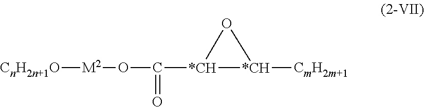
has been further added as the chiral compound of general formula (2-I), wherein each of n and m is an integer of 3 to 12, wherein n and m may be identical numerical values and M2 is a mesogenic and aromatic unit (mesogen) and represents a group selected from formulas (2-d)


wherein each of n and m is an integer of 3 to 12, wherein n and m may be identical numerical values, n and m in any of formula (2-IV) to formula (2-VIII) may be numerical values independent of each other, and M1 is defined identically to that of formula (2-IV) and may be identical to or different from that of formula (2-IV) or formula (2-V).
Claims (1)


Applications Claiming Priority (5)
| Application Number | Priority Date | Filing Date | Title |
|---|---|---|---|
| JP2006054850A JP2007231166A (en) | 2006-03-01 | 2006-03-01 | Liquid crystal element, optical path-deflecting element and image display device |
| JP2006054851A JP5261881B2 (en) | 2006-03-01 | 2006-03-01 | Liquid crystal element, optical path deflecting element, and image display apparatus |
| JP2006-054851 | 2006-03-01 | ||
| JP2006-054850 | 2006-03-01 | ||
| PCT/JP2007/054494 WO2007100150A1 (en) | 2006-03-01 | 2007-03-01 | Liquid crystal element, optical path deflecting element, and image displaying apparatus |
Publications (2)
| Publication Number | Publication Date |
|---|---|
| US20080204608A1 US20080204608A1 (en) | 2008-08-28 |
| US8158020B2 true US8158020B2 (en) | 2012-04-17 |
Family
ID=38459236
Family Applications (1)
| Application Number | Title | Priority Date | Filing Date |
|---|---|---|---|
| US11/913,378 Expired - Fee Related US8158020B2 (en) | 2006-03-01 | 2007-03-01 | Liquid crystal element, optical path deflecting element, and image displaying apparatus |
Country Status (4)
| Country | Link |
|---|---|
| US (1) | US8158020B2 (en) |
| EP (1) | EP1989276A4 (en) |
| KR (1) | KR20080011281A (en) |
| WO (1) | WO2007100150A1 (en) |
Cited By (1)
| Publication number | Priority date | Publication date | Assignee | Title |
|---|---|---|---|---|
| WO2018172232A1 (en) | 2017-03-21 | 2018-09-27 | Merck Patent Gmbh | Light modulation element |
Families Citing this family (6)
| Publication number | Priority date | Publication date | Assignee | Title |
|---|---|---|---|---|
| TWI589677B (en) * | 2011-11-15 | 2017-07-01 | 迪愛生股份有限公司 | Ferroelectric liquid crystal composition and ferroelectric liquid crystal display element |
| US20140313468A1 (en) * | 2011-11-18 | 2014-10-23 | Dic Corporation | Liquid crystal display element |
| JP5725260B2 (en) | 2012-06-06 | 2015-05-27 | Dic株式会社 | Liquid crystal light modulator |
| JP6496977B2 (en) | 2013-03-13 | 2019-04-10 | 株式会社リコー | Projection optical system and projector apparatus |
| EP3045968A1 (en) | 2015-01-16 | 2016-07-20 | Ricoh Company, Ltd. | Electrochromic apparatus, electrochromic element, and method of manufacturing electrochromic element |
| US20210261587A1 (en) * | 2020-01-30 | 2021-08-26 | The Regents Of The University Of California | STRAD-binding agents and Uses Thereof |
Citations (23)
| Publication number | Priority date | Publication date | Assignee | Title |
|---|---|---|---|---|
| JPH05279299A (en) | 1992-01-22 | 1993-10-26 | Hoechst Ag | 3-cyclohexylpropionic acid and used thereof in ferroelectric liquid crystal mixture |
| JPH05313116A (en) | 1992-05-14 | 1993-11-26 | Nippon Telegr & Teleph Corp <Ntt> | Projector |
| JPH0618940A (en) | 1992-06-30 | 1994-01-28 | Nippon Telegr & Teleph Corp <Ntt> | Optical beam shifter |
| JPH06206841A (en) | 1992-07-09 | 1994-07-26 | Hoechst Ag | Meta-substituted six-membered aromatic compound for using it for liquid crystal mixture |
| JPH06306363A (en) | 1993-04-10 | 1994-11-01 | Hoechst Ag | Smectic liquid crystal mixture |
| US5387371A (en) * | 1992-09-30 | 1995-02-07 | Merck Patent Gesellschaft Mit Beschrankter Haftung | Ferroelectric liquid-crystalline media, and their use in electro-optical devices |
| JPH0762349A (en) | 1993-07-22 | 1995-03-07 | Hoechst Ag | Smectic liquid crystal mixture |
| US5411668A (en) * | 1993-08-05 | 1995-05-02 | Poellmann; Klaus | Process for the reclamation of used glycolic aircraft deicing compositions |
| WO1997004039A1 (en) | 1995-07-17 | 1997-02-06 | Hoechst Research & Technology Deutschland Gmbh & Co. Kg | Ferroelectric liquid crystal mixture |
| JPH09133904A (en) | 1995-11-07 | 1997-05-20 | Oki Electric Ind Co Ltd | Optical deflection switch |
| WO1997024351A1 (en) | 1995-12-28 | 1997-07-10 | Hoechst Research & Technology Deutschland Gmbh & Co.Kg | Difluorophenyl pyrimidyl pyridine derivatives and the use thereof in liquid crystal mixtures |
| JPH10133135A (en) | 1996-10-31 | 1998-05-22 | Toshiba Corp | Light beam deflecting device |
| WO1999004383A1 (en) | 1997-07-18 | 1999-01-28 | Aventis Research & Technologies Gmbh & Co Kg | Ferroelectric liquid-crystal display with wide range of working temperatures |
| JP2939826B2 (en) | 1990-09-03 | 1999-08-25 | 日本電信電話株式会社 | Projection display device |
| JP3034024B2 (en) | 1989-03-22 | 2000-04-17 | ヘキスト・アクチェンゲゼルシャフト | Ferroelectric liquid crystal mixture with large spontaneous polarization and excellent orientation |
| US6280653B1 (en) * | 1997-09-17 | 2001-08-28 | Sharp Kabushiki Kaisha | Liquid crystal composition and liquid crystal shutter |
| JP2002328402A (en) | 2001-01-23 | 2002-11-15 | Ricoh Co Ltd | Method for deflecting light, deflecting element for light, deflecting device for light and image display device |
| JP2003280041A (en) | 2002-03-20 | 2003-10-02 | Ricoh Co Ltd | Light deflecting element, light deflector, and image display device |
| JP2004184522A (en) | 2002-11-29 | 2004-07-02 | Ricoh Co Ltd | Optical path deflector |
| JP3547015B2 (en) | 1993-01-07 | 2004-07-28 | ソニー株式会社 | Image display device and method for improving resolution of image display device |
| US6838128B1 (en) * | 2002-02-05 | 2005-01-04 | Displaytech, Inc. | High polarization dopants for ferroelectric liquid crystal compositions |
| JP2005338804A (en) | 2004-04-30 | 2005-12-08 | Ricoh Co Ltd | Optical axis deflection element, optical path deflection element, optical axis deflection method, optical path deflection method, optical axis deflection device, optical path deflection device, picture display device |
| US7304705B2 (en) * | 2002-03-26 | 2007-12-04 | Ricoh Company, Ltd. | Imaging unit, optical write unit, optical read unit and image forming apparatus |
-
2007
- 2007-03-01 KR KR1020077025427A patent/KR20080011281A/en not_active Application Discontinuation
- 2007-03-01 EP EP07715296A patent/EP1989276A4/en not_active Withdrawn
- 2007-03-01 WO PCT/JP2007/054494 patent/WO2007100150A1/en active Application Filing
- 2007-03-01 US US11/913,378 patent/US8158020B2/en not_active Expired - Fee Related
Patent Citations (24)
| Publication number | Priority date | Publication date | Assignee | Title |
|---|---|---|---|---|
| JP3034024B2 (en) | 1989-03-22 | 2000-04-17 | ヘキスト・アクチェンゲゼルシャフト | Ferroelectric liquid crystal mixture with large spontaneous polarization and excellent orientation |
| JP2939826B2 (en) | 1990-09-03 | 1999-08-25 | 日本電信電話株式会社 | Projection display device |
| JPH05279299A (en) | 1992-01-22 | 1993-10-26 | Hoechst Ag | 3-cyclohexylpropionic acid and used thereof in ferroelectric liquid crystal mixture |
| JPH05313116A (en) | 1992-05-14 | 1993-11-26 | Nippon Telegr & Teleph Corp <Ntt> | Projector |
| JPH0618940A (en) | 1992-06-30 | 1994-01-28 | Nippon Telegr & Teleph Corp <Ntt> | Optical beam shifter |
| JPH06206841A (en) | 1992-07-09 | 1994-07-26 | Hoechst Ag | Meta-substituted six-membered aromatic compound for using it for liquid crystal mixture |
| US5387371A (en) * | 1992-09-30 | 1995-02-07 | Merck Patent Gesellschaft Mit Beschrankter Haftung | Ferroelectric liquid-crystalline media, and their use in electro-optical devices |
| JP3547015B2 (en) | 1993-01-07 | 2004-07-28 | ソニー株式会社 | Image display device and method for improving resolution of image display device |
| JPH06306363A (en) | 1993-04-10 | 1994-11-01 | Hoechst Ag | Smectic liquid crystal mixture |
| US5441668A (en) * | 1993-04-10 | 1995-08-15 | Hoechst Aktiengesellschaft | Smectic liquid-crystal mixture |
| JPH0762349A (en) | 1993-07-22 | 1995-03-07 | Hoechst Ag | Smectic liquid crystal mixture |
| US5411668A (en) * | 1993-08-05 | 1995-05-02 | Poellmann; Klaus | Process for the reclamation of used glycolic aircraft deicing compositions |
| WO1997004039A1 (en) | 1995-07-17 | 1997-02-06 | Hoechst Research & Technology Deutschland Gmbh & Co. Kg | Ferroelectric liquid crystal mixture |
| JPH09133904A (en) | 1995-11-07 | 1997-05-20 | Oki Electric Ind Co Ltd | Optical deflection switch |
| WO1997024351A1 (en) | 1995-12-28 | 1997-07-10 | Hoechst Research & Technology Deutschland Gmbh & Co.Kg | Difluorophenyl pyrimidyl pyridine derivatives and the use thereof in liquid crystal mixtures |
| JPH10133135A (en) | 1996-10-31 | 1998-05-22 | Toshiba Corp | Light beam deflecting device |
| WO1999004383A1 (en) | 1997-07-18 | 1999-01-28 | Aventis Research & Technologies Gmbh & Co Kg | Ferroelectric liquid-crystal display with wide range of working temperatures |
| US6280653B1 (en) * | 1997-09-17 | 2001-08-28 | Sharp Kabushiki Kaisha | Liquid crystal composition and liquid crystal shutter |
| JP2002328402A (en) | 2001-01-23 | 2002-11-15 | Ricoh Co Ltd | Method for deflecting light, deflecting element for light, deflecting device for light and image display device |
| US6838128B1 (en) * | 2002-02-05 | 2005-01-04 | Displaytech, Inc. | High polarization dopants for ferroelectric liquid crystal compositions |
| JP2003280041A (en) | 2002-03-20 | 2003-10-02 | Ricoh Co Ltd | Light deflecting element, light deflector, and image display device |
| US7304705B2 (en) * | 2002-03-26 | 2007-12-04 | Ricoh Company, Ltd. | Imaging unit, optical write unit, optical read unit and image forming apparatus |
| JP2004184522A (en) | 2002-11-29 | 2004-07-02 | Ricoh Co Ltd | Optical path deflector |
| JP2005338804A (en) | 2004-04-30 | 2005-12-08 | Ricoh Co Ltd | Optical axis deflection element, optical path deflection element, optical axis deflection method, optical path deflection method, optical axis deflection device, optical path deflection device, picture display device |
Non-Patent Citations (2)
| Title |
|---|
| "Crystal Optics", Japan Society of Applied Physics, Optical Society of Japan, p. 198, 1975. |
| Pausch, Axel E. et al., "New Fluorinated Heterocyclic Compounds for Improved FLC-Mixtures", Proceedings SPIE The International Society for Optical Engineering, vol. 1665, pp. 128-133, 1992. |
Cited By (1)
| Publication number | Priority date | Publication date | Assignee | Title |
|---|---|---|---|---|
| WO2018172232A1 (en) | 2017-03-21 | 2018-09-27 | Merck Patent Gmbh | Light modulation element |
Also Published As
| Publication number | Publication date |
|---|---|
| WO2007100150A1 (en) | 2007-09-07 |
| KR20080011281A (en) | 2008-02-01 |
| EP1989276A4 (en) | 2011-03-02 |
| EP1989276A1 (en) | 2008-11-12 |
| US20080204608A1 (en) | 2008-08-28 |
Similar Documents
| Publication | Publication Date | Title |
|---|---|---|
| US8158020B2 (en) | Liquid crystal element, optical path deflecting element, and image displaying apparatus | |
| Kim et al. | Technical evolution of liquid crystal displays | |
| US8310636B2 (en) | Liquid crystal display device and polymer for aligning film material | |
| AU2007238392B9 (en) | High speed display shutter for autostereoscopic display | |
| US6885412B2 (en) | Liquid crystal display device, image shifting device, and image display apparatus | |
| CN101180567A (en) | Liquid crystal display element | |
| WO2008062744A1 (en) | Liquid crystal display element | |
| KR100191936B1 (en) | Liquid crystal composition, liquid crystal device using the composition, liquid crystal apparatus and display method | |
| US7489383B2 (en) | Optical axis deflecting method, optical axis deflecting element, optical path deflecting unit, method of driving optical axis deflecting element, and image display apparatus | |
| CN101321844B (en) | Liquid crystal element, optical path-deflecting element and image display device | |
| US8570481B2 (en) | Liquid crystal material, liquid crystal display device, liquid crystal optical space modulation device, and liquid crystal shutter | |
| JP4650408B2 (en) | Liquid crystal material, liquid crystal display device, and liquid crystal light spatial modulation device | |
| JP5261881B2 (en) | Liquid crystal element, optical path deflecting element, and image display apparatus | |
| US7838089B2 (en) | Liquid crystal material, liquid crystal display device and liquid crystal display | |
| US7943209B2 (en) | Liquid crystal molecule, liquid crystal display device, and liquid crystal spatial light modulation device | |
| JP2003280041A (en) | Light deflecting element, light deflector, and image display device | |
| TWI269103B (en) | Wide-view liquid crystal display device | |
| US7935395B2 (en) | Liquid crystal molecule, liquid crystal display device and liquid crystal optical spatial modulation device | |
| JP2002236297A (en) | Liquid crystal display device | |
| US20100079689A1 (en) | Liquid crystal molecule, liquid crystal display device and liquid crystal optical spatial modulation device | |
| JP2013147592A (en) | Ferroelectric liquid crystal composition and liquid crystal display element | |
| US20100085531A1 (en) | Liquid crystal molecule, liquid crystal material, liquid crystal display device and liquid crystal optical spatial modulation device | |
| JP2014019647A (en) | Compound, ferroelectric liquid crystal composition using the same and liquid crystal display | |
| Yoshihara et al. | A full-color video rate FLC display based on time domain color switching with a TFT array | |
| JP2002049060A (en) | Chiral smectic liquid crystal element |
Legal Events
| Date | Code | Title | Description |
|---|---|---|---|
| AS | Assignment |
Owner name: RICOH COMPANY, LTD., JAPAN Free format text: ASSIGNMENT OF ASSIGNORS INTEREST;ASSIGNORS:TAKANO, YOHEI;SUGIMOTO, HIROYUKI;TOKITA, TOSHIAKI;AND OTHERS;REEL/FRAME:020053/0915;SIGNING DATES FROM 20070810 TO 20070830 Owner name: RICOH COMPANY, LTD.,JAPAN Free format text: ASSIGNMENT OF ASSIGNORS INTEREST;ASSIGNORS:TAKANO, YOHEI;SUGIMOTO, HIROYUKI;TOKITA, TOSHIAKI;AND OTHERS;SIGNING DATES FROM 20070810 TO 20070830;REEL/FRAME:020053/0915 Owner name: RICOH COMPANY, LTD., JAPAN Free format text: ASSIGNMENT OF ASSIGNORS INTEREST;ASSIGNORS:TAKANO, YOHEI;SUGIMOTO, HIROYUKI;TOKITA, TOSHIAKI;AND OTHERS;SIGNING DATES FROM 20070810 TO 20070830;REEL/FRAME:020053/0915 |
|
| STCF | Information on status: patent grant |
Free format text: PATENTED CASE |
|
| FEPP | Fee payment procedure |
Free format text: PAYOR NUMBER ASSIGNED (ORIGINAL EVENT CODE: ASPN); ENTITY STATUS OF PATENT OWNER: LARGE ENTITY |
|
| FPAY | Fee payment |
Year of fee payment: 4 |
|
| FEPP | Fee payment procedure |
Free format text: MAINTENANCE FEE REMINDER MAILED (ORIGINAL EVENT CODE: REM.); ENTITY STATUS OF PATENT OWNER: LARGE ENTITY |
|
| LAPS | Lapse for failure to pay maintenance fees |
Free format text: PATENT EXPIRED FOR FAILURE TO PAY MAINTENANCE FEES (ORIGINAL EVENT CODE: EXP.); ENTITY STATUS OF PATENT OWNER: LARGE ENTITY |
|
| STCH | Information on status: patent discontinuation |
Free format text: PATENT EXPIRED DUE TO NONPAYMENT OF MAINTENANCE FEES UNDER 37 CFR 1.362 |
|
| FP | Lapsed due to failure to pay maintenance fee |
Effective date: 20200417 |