US8138044B2 - Method for manufacturing semiconductor flash memory and flash memory cell - Google Patents
Method for manufacturing semiconductor flash memory and flash memory cell Download PDFInfo
- Publication number
- US8138044B2 US8138044B2 US12/647,502 US64750209A US8138044B2 US 8138044 B2 US8138044 B2 US 8138044B2 US 64750209 A US64750209 A US 64750209A US 8138044 B2 US8138044 B2 US 8138044B2
- Authority
- US
- United States
- Prior art keywords
- spacer
- semiconductor substrate
- forming
- over
- flash memory
- Prior art date
- Legal status (The legal status is an assumption and is not a legal conclusion. Google has not performed a legal analysis and makes no representation as to the accuracy of the status listed.)
- Expired - Fee Related, expires
Links
- 239000004065 semiconductor Substances 0.000 title claims abstract description 52
- 238000000034 method Methods 0.000 title claims description 22
- 238000004519 manufacturing process Methods 0.000 title description 10
- 125000006850 spacer group Chemical group 0.000 claims abstract description 80
- 239000000758 substrate Substances 0.000 claims abstract description 45
- 229910021420 polycrystalline silicon Inorganic materials 0.000 claims abstract description 24
- 229920005591 polysilicon Polymers 0.000 claims abstract description 24
- 238000005530 etching Methods 0.000 claims description 15
- 238000000151 deposition Methods 0.000 claims description 8
- 238000005468 ion implantation Methods 0.000 claims description 5
- 239000002019 doping agent Substances 0.000 claims description 4
- 150000004767 nitrides Chemical class 0.000 claims description 4
- 238000000059 patterning Methods 0.000 claims description 4
- 239000007943 implant Substances 0.000 claims 1
- 239000011810 insulating material Substances 0.000 abstract description 5
- 230000001965 increasing effect Effects 0.000 description 6
- 230000008878 coupling Effects 0.000 description 5
- 238000010168 coupling process Methods 0.000 description 5
- 238000005859 coupling reaction Methods 0.000 description 5
- 238000001312 dry etching Methods 0.000 description 3
- 238000012986 modification Methods 0.000 description 3
- 230000004048 modification Effects 0.000 description 3
- BOTDANWDWHJENH-UHFFFAOYSA-N Tetraethyl orthosilicate Chemical compound CCO[Si](OCC)(OCC)OCC BOTDANWDWHJENH-UHFFFAOYSA-N 0.000 description 2
- 238000013500 data storage Methods 0.000 description 2
- 230000002708 enhancing effect Effects 0.000 description 2
- 229910052581 Si3N4 Inorganic materials 0.000 description 1
- 230000015572 biosynthetic process Effects 0.000 description 1
- 230000008021 deposition Effects 0.000 description 1
- 230000000694 effects Effects 0.000 description 1
- 230000005684 electric field Effects 0.000 description 1
- 230000006870 function Effects 0.000 description 1
- 238000002955 isolation Methods 0.000 description 1
- 230000007334 memory performance Effects 0.000 description 1
- 239000002184 metal Substances 0.000 description 1
- 238000007254 oxidation reaction Methods 0.000 description 1
- HQVNEWCFYHHQES-UHFFFAOYSA-N silicon nitride Chemical compound N12[Si]34N5[Si]62N3[Si]51N64 HQVNEWCFYHHQES-UHFFFAOYSA-N 0.000 description 1
Images


Classifications
-
- H—ELECTRICITY
- H01—ELECTRIC ELEMENTS
- H01L—SEMICONDUCTOR DEVICES NOT COVERED BY CLASS H10
- H01L21/00—Processes or apparatus adapted for the manufacture or treatment of semiconductor or solid state devices or of parts thereof
- H01L21/02—Manufacture or treatment of semiconductor devices or of parts thereof
- H01L21/04—Manufacture or treatment of semiconductor devices or of parts thereof the devices having potential barriers, e.g. a PN junction, depletion layer or carrier concentration layer
- H01L21/18—Manufacture or treatment of semiconductor devices or of parts thereof the devices having potential barriers, e.g. a PN junction, depletion layer or carrier concentration layer the devices having semiconductor bodies comprising elements of Group IV of the Periodic Table or AIIIBV compounds with or without impurities, e.g. doping materials
- H01L21/28—Manufacture of electrodes on semiconductor bodies using processes or apparatus not provided for in groups H01L21/20 - H01L21/268
- H01L21/28008—Making conductor-insulator-semiconductor electrodes
- H01L21/28017—Making conductor-insulator-semiconductor electrodes the insulator being formed after the semiconductor body, the semiconductor being silicon
- H01L21/28026—Making conductor-insulator-semiconductor electrodes the insulator being formed after the semiconductor body, the semiconductor being silicon characterised by the conductor
- H01L21/28123—Lithography-related aspects, e.g. sub-lithography lengths; Isolation-related aspects, e.g. to solve problems arising at the crossing with the side of the device isolation; Planarisation aspects
- H01L21/2815—Lithography-related aspects, e.g. sub-lithography lengths; Isolation-related aspects, e.g. to solve problems arising at the crossing with the side of the device isolation; Planarisation aspects part or whole of the electrode is a sidewall spacer or made by a similar technique, e.g. transformation under mask, plating
-
- H—ELECTRICITY
- H01—ELECTRIC ELEMENTS
- H01L—SEMICONDUCTOR DEVICES NOT COVERED BY CLASS H10
- H01L21/00—Processes or apparatus adapted for the manufacture or treatment of semiconductor or solid state devices or of parts thereof
- H01L21/02—Manufacture or treatment of semiconductor devices or of parts thereof
- H01L21/04—Manufacture or treatment of semiconductor devices or of parts thereof the devices having potential barriers, e.g. a PN junction, depletion layer or carrier concentration layer
- H01L21/18—Manufacture or treatment of semiconductor devices or of parts thereof the devices having potential barriers, e.g. a PN junction, depletion layer or carrier concentration layer the devices having semiconductor bodies comprising elements of Group IV of the Periodic Table or AIIIBV compounds with or without impurities, e.g. doping materials
- H01L21/26—Bombardment with radiation
- H01L21/263—Bombardment with radiation with high-energy radiation
- H01L21/265—Bombardment with radiation with high-energy radiation producing ion implantation
-
- H—ELECTRICITY
- H01—ELECTRIC ELEMENTS
- H01L—SEMICONDUCTOR DEVICES NOT COVERED BY CLASS H10
- H01L21/00—Processes or apparatus adapted for the manufacture or treatment of semiconductor or solid state devices or of parts thereof
- H01L21/02—Manufacture or treatment of semiconductor devices or of parts thereof
- H01L21/04—Manufacture or treatment of semiconductor devices or of parts thereof the devices having potential barriers, e.g. a PN junction, depletion layer or carrier concentration layer
- H01L21/18—Manufacture or treatment of semiconductor devices or of parts thereof the devices having potential barriers, e.g. a PN junction, depletion layer or carrier concentration layer the devices having semiconductor bodies comprising elements of Group IV of the Periodic Table or AIIIBV compounds with or without impurities, e.g. doping materials
- H01L21/28—Manufacture of electrodes on semiconductor bodies using processes or apparatus not provided for in groups H01L21/20 - H01L21/268
- H01L21/28008—Making conductor-insulator-semiconductor electrodes
- H01L21/28017—Making conductor-insulator-semiconductor electrodes the insulator being formed after the semiconductor body, the semiconductor being silicon
- H01L21/28026—Making conductor-insulator-semiconductor electrodes the insulator being formed after the semiconductor body, the semiconductor being silicon characterised by the conductor
- H01L21/28123—Lithography-related aspects, e.g. sub-lithography lengths; Isolation-related aspects, e.g. to solve problems arising at the crossing with the side of the device isolation; Planarisation aspects
- H01L21/28141—Lithography-related aspects, e.g. sub-lithography lengths; Isolation-related aspects, e.g. to solve problems arising at the crossing with the side of the device isolation; Planarisation aspects insulating part of the electrode is defined by a sidewall spacer, e.g. dummy spacer, or a similar technique, e.g. oxidation under mask, plating
-
- H—ELECTRICITY
- H01—ELECTRIC ELEMENTS
- H01L—SEMICONDUCTOR DEVICES NOT COVERED BY CLASS H10
- H01L21/00—Processes or apparatus adapted for the manufacture or treatment of semiconductor or solid state devices or of parts thereof
- H01L21/02—Manufacture or treatment of semiconductor devices or of parts thereof
- H01L21/04—Manufacture or treatment of semiconductor devices or of parts thereof the devices having potential barriers, e.g. a PN junction, depletion layer or carrier concentration layer
- H01L21/18—Manufacture or treatment of semiconductor devices or of parts thereof the devices having potential barriers, e.g. a PN junction, depletion layer or carrier concentration layer the devices having semiconductor bodies comprising elements of Group IV of the Periodic Table or AIIIBV compounds with or without impurities, e.g. doping materials
- H01L21/30—Treatment of semiconductor bodies using processes or apparatus not provided for in groups H01L21/20 - H01L21/26
- H01L21/31—Treatment of semiconductor bodies using processes or apparatus not provided for in groups H01L21/20 - H01L21/26 to form insulating layers thereon, e.g. for masking or by using photolithographic techniques; After treatment of these layers; Selection of materials for these layers
- H01L21/3105—After-treatment
- H01L21/31051—Planarisation of the insulating layers
-
- H—ELECTRICITY
- H01—ELECTRIC ELEMENTS
- H01L—SEMICONDUCTOR DEVICES NOT COVERED BY CLASS H10
- H01L29/00—Semiconductor devices specially adapted for rectifying, amplifying, oscillating or switching and having potential barriers; Capacitors or resistors having potential barriers, e.g. a PN-junction depletion layer or carrier concentration layer; Details of semiconductor bodies or of electrodes thereof ; Multistep manufacturing processes therefor
- H01L29/40—Electrodes ; Multistep manufacturing processes therefor
- H01L29/401—Multistep manufacturing processes
- H01L29/4011—Multistep manufacturing processes for data storage electrodes
- H01L29/40114—Multistep manufacturing processes for data storage electrodes the electrodes comprising a conductor-insulator-conductor-insulator-semiconductor structure
-
- H—ELECTRICITY
- H01—ELECTRIC ELEMENTS
- H01L—SEMICONDUCTOR DEVICES NOT COVERED BY CLASS H10
- H01L29/00—Semiconductor devices specially adapted for rectifying, amplifying, oscillating or switching and having potential barriers; Capacitors or resistors having potential barriers, e.g. a PN-junction depletion layer or carrier concentration layer; Details of semiconductor bodies or of electrodes thereof ; Multistep manufacturing processes therefor
- H01L29/40—Electrodes ; Multistep manufacturing processes therefor
- H01L29/41—Electrodes ; Multistep manufacturing processes therefor characterised by their shape, relative sizes or dispositions
- H01L29/423—Electrodes ; Multistep manufacturing processes therefor characterised by their shape, relative sizes or dispositions not carrying the current to be rectified, amplified or switched
- H01L29/42312—Gate electrodes for field effect devices
- H01L29/42316—Gate electrodes for field effect devices for field-effect transistors
- H01L29/4232—Gate electrodes for field effect devices for field-effect transistors with insulated gate
- H01L29/42324—Gate electrodes for transistors with a floating gate
-
- H—ELECTRICITY
- H01—ELECTRIC ELEMENTS
- H01L—SEMICONDUCTOR DEVICES NOT COVERED BY CLASS H10
- H01L29/00—Semiconductor devices specially adapted for rectifying, amplifying, oscillating or switching and having potential barriers; Capacitors or resistors having potential barriers, e.g. a PN-junction depletion layer or carrier concentration layer; Details of semiconductor bodies or of electrodes thereof ; Multistep manufacturing processes therefor
- H01L29/66—Types of semiconductor device ; Multistep manufacturing processes therefor
- H01L29/68—Types of semiconductor device ; Multistep manufacturing processes therefor controllable by only the electric current supplied, or only the electric potential applied, to an electrode which does not carry the current to be rectified, amplified or switched
- H01L29/76—Unipolar devices, e.g. field effect transistors
- H01L29/772—Field effect transistors
- H01L29/78—Field effect transistors with field effect produced by an insulated gate
- H01L29/788—Field effect transistors with field effect produced by an insulated gate with floating gate
- H01L29/7881—Programmable transistors with only two possible levels of programmation
-
- H—ELECTRICITY
- H10—SEMICONDUCTOR DEVICES; ELECTRIC SOLID-STATE DEVICES NOT OTHERWISE PROVIDED FOR
- H10B—ELECTRONIC MEMORY DEVICES
- H10B41/00—Electrically erasable-and-programmable ROM [EEPROM] devices comprising floating gates
- H10B41/30—Electrically erasable-and-programmable ROM [EEPROM] devices comprising floating gates characterised by the memory core region
Definitions
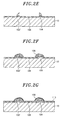
- a flash memory cell may have a double polysilicon structure such that information can be stored in and deleted from a specific cell.
- FIG. 1 illustrates an Electrically Erasable Programmable Read Only Memory (EEPROM) or a flash memory cell having a double polysilicon structure in a memory block.
- EEPROM Electrically Erasable Programmable Read Only Memory
- a flash memory cell of a double polysilicon structure has tunnel oxide film 12 , floating gate 14 , dielectric film 16 , control gate 18 , source region 20 , spacer 22 , and the like formed in that order on and/or over semiconductor substrate 10 . Accordingly, such a flash memory cell has two gates: floating gate 14 and control gate 18 . Floating gate 14 and control gate 18 are separated from each other by dielectric film 16 . Floating gate 14 and semiconductor substrate 10 are separated from each other by tunnel oxide film 12 .
- data storage is implemented by injecting electrons or holes into floating gate 14 or by erasing electrons or holes from floating gate 14 .
- floating gate 14 is completely separated by tunnel oxide film 12 and dielectric film 16 , e.g., an Oxide+Nitride+Oxide (ONO) dielectric film, electrons or holes injected into floating gate 14 do not escape floating gate 14 even if power is not supplied, such that data is not lost.
- a bias applied to an externally accessible terminal, i.e., control gate 18 and the junction or substrate 10 can be induced to floating gate 14 , so that a large electric field can be formed between both ends of tunnel oxide film 12 .
- a ratio of the voltage applied to control gate 18 and the junction or substrate 10 and induced to floating gate 14 is referred to as a coupling ratio (CR).
- CR coupling ratio
- control gate 18 is an electrode that functions as a gate of a nonvolatile memory having a polysilicon stacked structure. Programming and erasure for cells are performed according to the bias state of this electrode. Generally, after such a gate is etched, the dielectric film is etched.
- a process for manufacturing such a semiconductor flash memory is described as follows. First, tunnel oxide film 12 and polysilicon for floating gate 14 are deposited on and/or over semiconductor substrate 10 . A silicon nitride film, e.g., tetraethylorthosilicate (TEOS) layer is etched. Polysilicon is then deposited on and/or over the polysilicon for floating gate 14 to form control gate 18 , and then a control gate pattern is formed. Control gate 18 is etched so that spacer 22 is formed by an etch-back effect. Polysilicon is etched by using an etching selectivity of an oxide film and polysilicon. When spacer 22 is removed, the underlying oxide film and nitride film are removed. In this case, an ONO step is formed between two layers of polysilicon. Finally, ONO is etched again to remove the ONO at sidewall.
- TEOS tetraethylorthosilicate
- the flash memory cell programming or erasure is performed in accordance with presence/absence of electrons in the floating gate on the gate oxide film.
- the floating gate is insulated by the ONO structure or a similar structure, and the control gate is deposited as an upper electrode. Programming or erasure of cells is determined by the bias applied to the control gate.
- To increase the operation speed of such a flash memory cell it is necessary to reduce a cell size, but it is difficult to reduce the cell size since a general transistor is used, as illustrated in FIG. 1 . Nevertheless, it is very important to reduce the area of the flash memory cell for increasing the entire memory density and the memory operation speed thereby enhancing memory performance.
- Embodiments relate to a flash memory cell and a method of manufacturing a semiconductor flash memory for reducing a cell size to increase a memory operation speed.
- Embodiments relate to a flash memory cell and a method of manufacturing a semiconductor flash memory that reduces the size of a floating gate by using sidewall polysilicon as the floating gate, thereby reducing a cell size and increasing a coupling ratio to the floating gate.
- a method of manufacturing a semiconductor flash memory can include at least one of the following: forming a hard mask pattern by depositing an oxide film on and/or over a semiconductor substrate and performing patterning and etching thereto; forming a tunnel oxide film on and/or over the semiconductor substrate having the hard mask pattern formed thereon and/or thereover; depositing polysilicon on and/or over the hard mask pattern on and/or over which the tunnel oxide film has been formed and performing etching to form a first spacer at the sidewall of the hard mask pattern; partially removing the hard mask pattern and the tunnel oxide film and forming a source/drain region self-aligned with the first spacer; and then forming a second spacer at the sidewall of the first spacer.
- a method of manufacturing a semiconductor flash memory can include at least one of the following: forming a hard mask pattern by depositing an oxide film over a semiconductor substrate and performing patterning and a first etching process on the oxide film; forming a tunnel oxide film over the semiconductor substrate including the hard mask; forming a first spacer serving as a floating gate at sidewalls of the hard mask by depositing a first polysilicon layer over the semiconductor substrate, the hard mask pattern and the tunnel oxide film and then performing a second etching process; performing a third etching process removing the hard mask pattern and a portion of the tunnel oxide film; forming a source/drain region self-aligned with the first spacer by conducting a first ion-implantation process on the semiconductor substrate; and then forming a second spacer at sidewalls of the first spacer by forming an insulating layer over the entire surface of the semiconductor substrate and then performing a fourth etching process on the insulating layer.
- a flash memory cell can include at least one of the following: a semiconductor substrate; a tunnel oxide film formed on and/or over the semiconductor substrate; a first spacer formed on and/or over the semiconductor substrate having the tunnel oxide film formed thereon and/or thereover; a second spacer formed at the sidewall of the first spacer; a dielectric film formed at upper portions of the first spacer and the second spacer; a control gate formed at an upper portion of the dielectric film; and a third spacer formed at the sidewalls of the control gate and the second spacer.
- a flash memory cell can include at least one of the following: a semiconductor substrate; a tunnel oxide film formed over the semiconductor substrate; a first spacer composed of polysilicon formed over the semiconductor substrate including the tunnel oxide film; a second spacer composed of an insulating material formed at sidewalls of the first spacer; a dielectric film formed at the uppermost surface of the first spacer and the second spacer; a control gate formed at the uppermost surface of the dielectric film; and a third spacer composed of an insulating material formed at and contacting sidewalls of the second spacer, the dielectric film and the control gate.
- a flash memory cell can include at least one of the following: a semiconductor substrate; an insulating film pattern formed over and contacting the semiconductor substrate; a first spacer composed of polysilicon formed over and contacting the insulating film pattern film; a second spacer formed over and contacting sidewalls of the first spacer; a dielectric film formed over and contacting the uppermost surface of the first spacer and the second spacer; a control gate formed over and contacting the uppermost surface of the dielectric film; a third spacer formed over and contacting sidewalls of the second spacer, the dielectric film and the control gate; a first source/drain region formed in the semiconductor substrate and self-aligned with the first spacer; and a second source/drain region formed in the semiconductor substrate and self-aligned with the second spacer.
- the floating gate of the flash memory can be reduced in size, thereby increasing the operation speed of cells and reducing a delay time. Further, a voltage applied to the floating gate can be reduced, thereby increasing operation efficiency and enhancing reliability characteristics. As the floating gate is reduced in size, a coupling ratio of a bias applied from the control gate to be induced to the floating gate can be increased.
- FIG. 1 is a process sectional view illustrating a method of manufacturing a semiconductor flash memory.
- FIGS. 2A to 2J are process sectional views illustrating a method of manufacturing a semiconductor flash memory in accordance with embodiments.
- FIGS. 2A to 2J are process sectional views illustrating a method of manufacturing a semiconductor flash memory, in accordance with embodiments.
- an oxide film to serve as a hard mask is deposited on and/or over semiconductor substrate 10 , and patterned and etched to form hard mask pattern 100 .
- thermal oxidization is performed on and/or over semiconductor substrate 10 including hard mask pattern 100 formed thereon to form tunnel oxide film 102 .
- a first polysilicon layer is deposited on and/or over hard mask pattern 100 including tunnel oxide film 102 .
- Etching is then performed to form first spacer 104 composed of polysilicon at sidewalls of hard mask pattern 100 .
- First spacer 104 may correspond to a floating gate of a flash memory cell, as described below.
- First spacer 104 is referred to as a spacer for a floating gate.
- hard mask pattern 100 and a portion of tunnel oxide film 102 are removed using, e.g., dry etching. After the etching, a portion of a tunnel oxide film 102 ′ remains under first spacer 104 interposed between first spacer 104 and semiconductor substrate 10 .
- an N-type dopant is ion-implanted in semiconductor substrate 10 to form source/drain region 106 .
- Shallow ion implantation may be performed to lower the level of a current leak and to also induce hot carrier generation.
- Source/drain region 106 may be formed relatively deep at a time by appropriately controlling ion dosage and energy. If a current leak results, an LDD ion implantation for CMOS may be performed.
- a sidewall process is performed on the sidewalls of first spacer 104 of the floating gate.
- an insulating material is formed on and/or over the entire surface of substrate 10 and etched by dry etching to form second spacer 108 at the sidewalls of first spacer 104 and overlapping a corresponding source/drain region 106 .
- Second spacer 108 is formed to maintain flatness of the floating gate and ensure a sufficient thickness for sidewall deposition.
- a dielectric film e.g., Oxide/Nitride/Oxide (ONO) dielectric film 110 is formed on and/or over the entire surface of semiconductor substrate 10 including first spacer 104 , source/drain region 106 and second spacer 108 .
- ONO dielectric film 110 should be formed to insulate a floating gate and a control gate described below.
- a second polysilicon layer for forming a gate electrode is deposited over the entire surface of semiconductor substrate 10 .
- the second polysilicon layer is then patterned and etched to thereby form control gate 112 .
- a portion of second spacer 108 and ONO dielectric film 110 are also etched during formation of control fate 12 such that respective portions second spacer 108 ′ and ONO dielectric film 110 ′ remain.
- a conductive dopant is ion-implanted with low concentration to form source/drain region 114 self-aligned with second spacer 108 ′.
- an insulating film is then formed on and/or over the entire surface of substrate 10 and etched by dry etching to form third spacer 116 at the sidewalls of second spacer 108 ′, ONO dielectric film 110 ′ and control electrode 112 . Thereafter, a dopant is implanted between device isolation films to form a photodiode. Multilayered metal interconnects are connected to each other through a via.
- a flash memory cell implemented by the method of manufacturing a semiconductor flash memory in accordance with embodiments includes semiconductor substrate 10 , tunnel oxide film 102 ′ and first spacer 104 serving as a floating gate sequentially formed on and/or over semiconductor substrate 10 , first source/drain region 106 self-aligned with first spacer 104 in semiconductor substrate 10 , second spacer 108 ′ formed at the sidewalls of first spacer 104 , ONO dielectric film 110 ′ formed on and/or over the uppermost surface of first spacer 104 and second spacer 108 ′, control gate 112 formed on and/or over the uppermost surface of ONO dielectric film 110 ′, second source/drain region 114 self-aligned with second spacer 108 ′, and third spacer 116 formed at the sidewalls of control gate 112 and second spacer 108 ′.
- the floating gate can be reduced in size by using sidewall polysilicon as the floating gate, thereby reducing the cell size and increasing the coupling ratio to the floating gate.
Landscapes
- Engineering & Computer Science (AREA)
- Microelectronics & Electronic Packaging (AREA)
- Power Engineering (AREA)
- Physics & Mathematics (AREA)
- Condensed Matter Physics & Semiconductors (AREA)
- General Physics & Mathematics (AREA)
- Computer Hardware Design (AREA)
- Ceramic Engineering (AREA)
- Manufacturing & Machinery (AREA)
- High Energy & Nuclear Physics (AREA)
- Health & Medical Sciences (AREA)
- Toxicology (AREA)
- Non-Volatile Memory (AREA)
- Semiconductor Memories (AREA)
Abstract
Description
Claims (3)
Applications Claiming Priority (2)
| Application Number | Priority Date | Filing Date | Title |
|---|---|---|---|
| KR1020080137574A KR20100079159A (en) | 2008-12-30 | 2008-12-30 | Method for manufacturing semiconductor flash memory, flash memory cell |
| KR10-2008-0137574 | 2008-12-30 |
Publications (2)
| Publication Number | Publication Date |
|---|---|
| US20100163961A1 US20100163961A1 (en) | 2010-07-01 |
| US8138044B2 true US8138044B2 (en) | 2012-03-20 |
Family
ID=42283795
Family Applications (1)
| Application Number | Title | Priority Date | Filing Date |
|---|---|---|---|
| US12/647,502 Expired - Fee Related US8138044B2 (en) | 2008-12-30 | 2009-12-27 | Method for manufacturing semiconductor flash memory and flash memory cell |
Country Status (2)
| Country | Link |
|---|---|
| US (1) | US8138044B2 (en) |
| KR (1) | KR20100079159A (en) |
Families Citing this family (1)
| Publication number | Priority date | Publication date | Assignee | Title |
|---|---|---|---|---|
| US11257963B1 (en) | 2020-11-20 | 2022-02-22 | Taiwan Semiconductor Manufacturing Company, Ltd. | Semiconductor device |
Citations (3)
| Publication number | Priority date | Publication date | Assignee | Title |
|---|---|---|---|---|
| US20020145167A1 (en) * | 1997-03-14 | 2002-10-10 | Toru Yamazaki | A bicmos device having a cmos gate electrode and a bipolar emitter each containing two imurities of the same conductivity type |
| US20090309226A1 (en) * | 2008-06-16 | 2009-12-17 | International Business Machines Corporation | Interconnect Structure for Electromigration Enhancement |
| US20100029052A1 (en) * | 2008-07-29 | 2010-02-04 | Kang Sung-Taeg | Self-aligned in-laid split gate memory and method of making |
-
2008
- 2008-12-30 KR KR1020080137574A patent/KR20100079159A/en not_active Application Discontinuation
-
2009
- 2009-12-27 US US12/647,502 patent/US8138044B2/en not_active Expired - Fee Related
Patent Citations (3)
| Publication number | Priority date | Publication date | Assignee | Title |
|---|---|---|---|---|
| US20020145167A1 (en) * | 1997-03-14 | 2002-10-10 | Toru Yamazaki | A bicmos device having a cmos gate electrode and a bipolar emitter each containing two imurities of the same conductivity type |
| US20090309226A1 (en) * | 2008-06-16 | 2009-12-17 | International Business Machines Corporation | Interconnect Structure for Electromigration Enhancement |
| US20100029052A1 (en) * | 2008-07-29 | 2010-02-04 | Kang Sung-Taeg | Self-aligned in-laid split gate memory and method of making |
Also Published As
| Publication number | Publication date |
|---|---|
| US20100163961A1 (en) | 2010-07-01 |
| KR20100079159A (en) | 2010-07-08 |
Similar Documents
| Publication | Publication Date | Title |
|---|---|---|
| US8076201B2 (en) | Method of manufacturing flash memory device | |
| JP2007281092A (en) | Semiconductor device, and manufacturing method thereof | |
| JP2007524233A (en) | Embedded channel flash structure to reduce short channel effects | |
| US8058162B2 (en) | Nonvolatile semiconductor memory and method of manufacturing the same | |
| US8546866B2 (en) | Nonvolatile semiconductor memory device capable of preventing a silicide short | |
| US6794710B2 (en) | Split-gate flash memory structure and method of manufacture | |
| US6743676B2 (en) | Method of forming a floating gate in a flash memory device | |
| CN100377335C (en) | Method for fabricating flash memory device | |
| KR100809338B1 (en) | Semiconductor device and method of fabricating the same | |
| JP5998512B2 (en) | Semiconductor device and manufacturing method of semiconductor device | |
| US20090026581A1 (en) | Flash memory device and method of manufacturing the same | |
| US20070155098A1 (en) | Method of manufacturing NAND flash memory device | |
| US20060006453A1 (en) | Nonvolatile semiconductor memory device and method of fabricating the same | |
| US20230232623A1 (en) | Method of manufacturing non-volatile memory device | |
| US8138044B2 (en) | Method for manufacturing semiconductor flash memory and flash memory cell | |
| KR100557531B1 (en) | Semiconductor device and method for manufacturing the same | |
| US7635629B2 (en) | Method of manufacturing non-volatile memory device | |
| WO2007000808A1 (en) | Semiconductor device and fabrication method thereof | |
| KR100654359B1 (en) | Method for fabricating nonvolatible memory device | |
| US7875924B2 (en) | Flash memory device and method for fabricating the same | |
| US20080254584A1 (en) | Method of manufacturing flash memory device | |
| KR20080069481A (en) | Nonvolatile memory device having buried type split gate and method of fabricating the same | |
| KR100889923B1 (en) | Flash memory device and method for fabricating the same | |
| TWI823398B (en) | Non-volatile memory device | |
| KR100732391B1 (en) | Method for forming and motion of read only memory |
Legal Events
| Date | Code | Title | Description |
|---|---|---|---|
| AS | Assignment |
Owner name: DONGBU HITEK CO., LTD.,KOREA, REPUBLIC OF Free format text: ASSIGNMENT OF ASSIGNORS INTEREST;ASSIGNOR:KIM, HYUN-TAE;REEL/FRAME:023704/0630 Effective date: 20091222 Owner name: DONGBU HITEK CO., LTD., KOREA, REPUBLIC OF Free format text: ASSIGNMENT OF ASSIGNORS INTEREST;ASSIGNOR:KIM, HYUN-TAE;REEL/FRAME:023704/0630 Effective date: 20091222 |
|
| ZAAA | Notice of allowance and fees due |
Free format text: ORIGINAL CODE: NOA |
|
| ZAAB | Notice of allowance mailed |
Free format text: ORIGINAL CODE: MN/=. |
|
| STCF | Information on status: patent grant |
Free format text: PATENTED CASE |
|
| FEPP | Fee payment procedure |
Free format text: PAYOR NUMBER ASSIGNED (ORIGINAL EVENT CODE: ASPN); ENTITY STATUS OF PATENT OWNER: LARGE ENTITY |
|
| FEPP | Fee payment procedure |
Free format text: PAT HOLDER CLAIMS SMALL ENTITY STATUS, ENTITY STATUS SET TO SMALL (ORIGINAL EVENT CODE: LTOS); ENTITY STATUS OF PATENT OWNER: LARGE ENTITY |
|
| FEPP | Fee payment procedure |
Free format text: PAYOR NUMBER ASSIGNED (ORIGINAL EVENT CODE: ASPN); ENTITY STATUS OF PATENT OWNER: LARGE ENTITY Free format text: PAYER NUMBER DE-ASSIGNED (ORIGINAL EVENT CODE: RMPN); ENTITY STATUS OF PATENT OWNER: LARGE ENTITY |
|
| AS | Assignment |
Owner name: INPHI CORPORATION, UNITED STATES Free format text: ASSIGNMENT OF ASSIGNORS INTEREST;ASSIGNOR:DONGBU HITEK, CO., LTD.;REEL/FRAME:034009/0157 Effective date: 20141008 |
|
| AS | Assignment |
Owner name: INPHI CORPORATION, CALIFORNIA Free format text: CORRECTIVE ASSIGNMENT TO CORRECT REMOVE PATENT NO. 878209 FROM EXHIBIT B PREVIOUSLY RECORDED AT REEL: 034009 FRAME: 0157. ASSIGNOR(S) HEREBY CONFIRMS THE ASSIGNMENT;ASSIGNOR:DONGBU HITEK, CO., LTD.;REEL/FRAME:034087/0097 Effective date: 20141008 |
|
| FEPP | Fee payment procedure |
Free format text: PAYOR NUMBER ASSIGNED (ORIGINAL EVENT CODE: ASPN); ENTITY STATUS OF PATENT OWNER: LARGE ENTITY Free format text: PAYER NUMBER DE-ASSIGNED (ORIGINAL EVENT CODE: RMPN); ENTITY STATUS OF PATENT OWNER: LARGE ENTITY |
|
| FPAY | Fee payment |
Year of fee payment: 4 |
|
| AS | Assignment |
Owner name: INPHI CORPORATION, CALIFORNIA Free format text: ASSIGNMENT OF ASSIGNORS INTEREST;ASSIGNOR:DONGBU HITEK, CO., LTD.;REEL/FRAME:041375/0062 Effective date: 20141008 |
|
| FEPP | Fee payment procedure |
Free format text: ENTITY STATUS SET TO UNDISCOUNTED (ORIGINAL EVENT CODE: BIG.) |
|
| MAFP | Maintenance fee payment |
Free format text: PAYMENT OF MAINTENANCE FEE, 8TH YEAR, LARGE ENTITY (ORIGINAL EVENT CODE: M1552); ENTITY STATUS OF PATENT OWNER: LARGE ENTITY Year of fee payment: 8 |
|
| AS | Assignment |
Owner name: MARVELL TECHNOLOGY CAYMAN I, CAYMAN ISLANDS Free format text: ASSIGNMENT OF ASSIGNORS INTEREST;ASSIGNOR:INPHI CORPORATION;REEL/FRAME:056649/0823 Effective date: 20210617 |
|
| AS | Assignment |
Owner name: CAVIUM INTERNATIONAL, CAYMAN ISLANDS Free format text: ASSIGNMENT OF ASSIGNORS INTEREST;ASSIGNOR:MARVELL TECHNOLOGY CAYMAN I;REEL/FRAME:057279/0519 Effective date: 20210620 |
|
| AS | Assignment |
Owner name: MARVELL ASIA PTE LTD., SINGAPORE Free format text: ASSIGNMENT OF ASSIGNORS INTEREST;ASSIGNOR:CAVIUM INTERNATIONAL;REEL/FRAME:057336/0873 Effective date: 20210620 |
|
| FEPP | Fee payment procedure |
Free format text: MAINTENANCE FEE REMINDER MAILED (ORIGINAL EVENT CODE: REM.); ENTITY STATUS OF PATENT OWNER: LARGE ENTITY |
|
| LAPS | Lapse for failure to pay maintenance fees |
Free format text: PATENT EXPIRED FOR FAILURE TO PAY MAINTENANCE FEES (ORIGINAL EVENT CODE: EXP.); ENTITY STATUS OF PATENT OWNER: LARGE ENTITY |
|
| STCH | Information on status: patent discontinuation |
Free format text: PATENT EXPIRED DUE TO NONPAYMENT OF MAINTENANCE FEES UNDER 37 CFR 1.362 |
|
| FP | Lapsed due to failure to pay maintenance fee |
Effective date: 20240320 |