US8119258B2 - White organic light emitting device (OLED) - Google Patents
White organic light emitting device (OLED) Download PDFInfo
- Publication number
- US8119258B2 US8119258B2 US12/213,356 US21335608A US8119258B2 US 8119258 B2 US8119258 B2 US 8119258B2 US 21335608 A US21335608 A US 21335608A US 8119258 B2 US8119258 B2 US 8119258B2
- Authority
- US
- United States
- Prior art keywords
- light emitting
- white oled
- emitting layer
- layer
- anode
- Prior art date
- Legal status (The legal status is an assumption and is not a legal conclusion. Google has not performed a legal analysis and makes no representation as to the accuracy of the status listed.)
- Active, expires
Links
Images


Classifications
-
- H—ELECTRICITY
- H10—SEMICONDUCTOR DEVICES; ELECTRIC SOLID-STATE DEVICES NOT OTHERWISE PROVIDED FOR
- H10K—ORGANIC ELECTRIC SOLID-STATE DEVICES
- H10K50/00—Organic light-emitting devices
- H10K50/10—OLEDs or polymer light-emitting diodes [PLED]
- H10K50/11—OLEDs or polymer light-emitting diodes [PLED] characterised by the electroluminescent [EL] layers
- H10K50/125—OLEDs or polymer light-emitting diodes [PLED] characterised by the electroluminescent [EL] layers specially adapted for multicolour light emission, e.g. for emitting white light
-
- H—ELECTRICITY
- H05—ELECTRIC TECHNIQUES NOT OTHERWISE PROVIDED FOR
- H05B—ELECTRIC HEATING; ELECTRIC LIGHT SOURCES NOT OTHERWISE PROVIDED FOR; CIRCUIT ARRANGEMENTS FOR ELECTRIC LIGHT SOURCES, IN GENERAL
- H05B33/00—Electroluminescent light sources
- H05B33/12—Light sources with substantially two-dimensional radiating surfaces
- H05B33/14—Light sources with substantially two-dimensional radiating surfaces characterised by the chemical or physical composition or the arrangement of the electroluminescent material, or by the simultaneous addition of the electroluminescent material in or onto the light source
-
- H—ELECTRICITY
- H05—ELECTRIC TECHNIQUES NOT OTHERWISE PROVIDED FOR
- H05B—ELECTRIC HEATING; ELECTRIC LIGHT SOURCES NOT OTHERWISE PROVIDED FOR; CIRCUIT ARRANGEMENTS FOR ELECTRIC LIGHT SOURCES, IN GENERAL
- H05B33/00—Electroluminescent light sources
- H05B33/12—Light sources with substantially two-dimensional radiating surfaces
- H05B33/20—Light sources with substantially two-dimensional radiating surfaces characterised by the chemical or physical composition or the arrangement of the material in which the electroluminescent material is embedded
-
- H—ELECTRICITY
- H10—SEMICONDUCTOR DEVICES; ELECTRIC SOLID-STATE DEVICES NOT OTHERWISE PROVIDED FOR
- H10K—ORGANIC ELECTRIC SOLID-STATE DEVICES
- H10K50/00—Organic light-emitting devices
-
- H—ELECTRICITY
- H10—SEMICONDUCTOR DEVICES; ELECTRIC SOLID-STATE DEVICES NOT OTHERWISE PROVIDED FOR
- H10K—ORGANIC ELECTRIC SOLID-STATE DEVICES
- H10K50/00—Organic light-emitting devices
- H10K50/10—OLEDs or polymer light-emitting diodes [PLED]
- H10K50/17—Carrier injection layers
- H10K50/171—Electron injection layers
-
- H—ELECTRICITY
- H10—SEMICONDUCTOR DEVICES; ELECTRIC SOLID-STATE DEVICES NOT OTHERWISE PROVIDED FOR
- H10K—ORGANIC ELECTRIC SOLID-STATE DEVICES
- H10K2101/00—Properties of the organic materials covered by group H10K85/00
- H10K2101/30—Highest occupied molecular orbital [HOMO], lowest unoccupied molecular orbital [LUMO] or Fermi energy values
-
- H—ELECTRICITY
- H10—SEMICONDUCTOR DEVICES; ELECTRIC SOLID-STATE DEVICES NOT OTHERWISE PROVIDED FOR
- H10K—ORGANIC ELECTRIC SOLID-STATE DEVICES
- H10K85/00—Organic materials used in the body or electrodes of devices covered by this subclass
- H10K85/10—Organic polymers or oligomers
- H10K85/111—Organic polymers or oligomers comprising aromatic, heteroaromatic, or aryl chains, e.g. polyaniline, polyphenylene or polyphenylene vinylene
- H10K85/113—Heteroaromatic compounds comprising sulfur or selene, e.g. polythiophene
- H10K85/1135—Polyethylene dioxythiophene [PEDOT]; Derivatives thereof
-
- Y—GENERAL TAGGING OF NEW TECHNOLOGICAL DEVELOPMENTS; GENERAL TAGGING OF CROSS-SECTIONAL TECHNOLOGIES SPANNING OVER SEVERAL SECTIONS OF THE IPC; TECHNICAL SUBJECTS COVERED BY FORMER USPC CROSS-REFERENCE ART COLLECTIONS [XRACs] AND DIGESTS
- Y10—TECHNICAL SUBJECTS COVERED BY FORMER USPC
- Y10S—TECHNICAL SUBJECTS COVERED BY FORMER USPC CROSS-REFERENCE ART COLLECTIONS [XRACs] AND DIGESTS
- Y10S428/00—Stock material or miscellaneous articles
- Y10S428/917—Electroluminescent
Definitions
- the present invention relates to an Organic Light Emitting Device (OLED), and more particularly, the present invention relates to a white OLED having stabilized colors and improved light emitting efficiency.
- OLED Organic Light Emitting Device
- OLEDs are light emitting devices that use a phenomenon whereby light is generated by combining an electron and a hole in an organic light emitting layer when a current or voltage is supplied in the organic light emitting layer.
- an OLED may have a multi-layer structure in which a Hole Injection Layer (HIL) and a Hole Transporting Layer (HTL) are formed between an anode electrode and the organic light emitting layer and an Electron Injection Layer (EIL) and an Electron Transporting Layer (ETL) are formed between a cathode electrode and the organic light emitting layer.
- HIL Hole Injection Layer
- HTL Hole Transporting Layer
- EIL Electron Injection Layer
- ETL Electron Transporting Layer
- the driving voltage of the OLED is approximately 5 V so that low voltage driving of the OLED is possible. Also, surface emitting with high brightness, quick response speed, and a thinner OLED are realizable. In addition to this, color reproduction is excellent, wide viewing angles are available, and emitted colors can be easily changed by appropriate selection of fluorescent materials. Accordingly, OLEDs can be used in various fields, such as full color display devices, backlight units for Liquid Crystal Displays (LCDs), information display devices, vehicle display devices, and lighting devices.
- LCDs Liquid Crystal Displays
- the white OLED emits white light and has a structure in which light emitting layers of predetermined colors are stacked therein.
- a white OLED can be applied to, in particular, a paper-thin light source, a backlight unit for an LCD, and full color display devices employing a color filter.
- the materials forming the light emitting layers of each color are different in the white OLED, if a current injected into the white OLED is changed, stable colors cannot be realized.
- light is generated from the light emitting layers of each color in the white OLED so that the light emitting efficiency of the white LCD is lower than that of the OLED including a light emitting layer of a single color.
- the present invention provides a white Organic Light Emitting Device (OLED) having stabilized colors and improved light emitting efficiency.
- OLED Organic Light Emitting Device
- a white Organic Light Emitting Device including: an anode and cathode spaced apart from each other; first, second, and third light emitting layers that are sequentially stacked between the anode and the cathode; and an electron injection induction layer, arranged between the second light emitting layer and the third light emitting layer, to induce electrons to flow into the second light emitting layer from the third light emitting layer.
- a difference between a Lowest Occupied Molecular Orbital (LUMO) energy level of the electron injection induction layer and the LUMO energy level of a dopant in the second light emitting layer is 0.4 eV or below.
- LUMO Lowest Occupied Molecular Orbital
- the electron injection induction layer may be formed of a material having an excellent hole transporting property and electron transporting property.
- the electron injection induction layer may be formed of a carbazole, the carbazole compound including 4,4-N,N′-dicarbazole-biphenyl (CBP), a CBP derivative, N,N′-dicarbazolyl3,5-benzene (mCP), or a mCP derivative.
- CBP 4,4-N,N′-dicarbazole-biphenyl
- mCP N,N′-dicarbazolyl3,5-benzene
- the electron injection induction layer may be formed to have a thickness of 1-10 nm.
- the first, second, and third light emitting layers may be, respectively, red, green, and blue light emitting layers.
- the first and second light emitting layers may include a host material having a better hole transporting property than an electron transporting property.
- the first light emitting layer may include a host material formed of a triphenylamine derivative, the triphenylamine derivative including N,N′-diphenyl-N,N′-bis(3-methylphenyl)-1,1′-bi-phenyl-4,4′-diamine (TPD) or N,N′-di(naphthalen-1-yl)-N,N′-diphenyl-benzidine (NPB).
- TPD N,N′-di(naphthalen-1-yl)-N,N′-diphenyl-benzidine
- the second light emitting layer may include a host material formed of a triphenylamine derivative or a carbazole compound.
- the third light emitting layer may include a fluorescent host material having an excellent hole transporting property and electron transporting property or a phosphorescent host material having a better electron transporting property than a hole transporting property.
- the first, second, and third light emitting layers may be, respectively, formed to have a thickness of 1-20 nm.
- the white OLED may further include: a hole transporting layer (HTL) between the anode and the first light emitting layer; and an electron transporting layer (ETL) between the cathode and the third light emitting layer.
- HTL hole transporting layer
- ETL electron transporting layer
- the HTL may be formed of N,N′-diphenyl-N,N′-bis(3-methylphenyl)-1,1′-bi-phenyl-4,4′-diamine (TPD) or N,N′-di(naphthalen-1-yl)-N,N′-diphenyl-benzidine (NPB).
- TPD N,N′-di(naphthalen-1-yl)-N,N′-diphenyl-benzidine
- the ETL may be formed of an aryl compound, the aryl compound may include: oxadiazole, triazole, phenanthroline, benzoxazole, or benzthiazole.
- the white OLED may further include a Hole Injecting Layer (HIL) between the anode and the HTL and an Electron Injecting Layer (EIL) between the cathode and the ETL.
- HIL may be formed of 4,4′,4′′-tris(3-methylphenylphenylamino)triphenylamine (MTDATA), copper phthalocyanine (CuPc), or poly(3,4-ethylenedioxythiphene, polystyrene sulfonated (PEDOT/PSS).
- the EIL may be formed of Lithium Fluoride (LIF) or Lithium Quinolate (LiQ).
- the anode may be formed of a material having a work function of 4.7 eV or above.
- the anode may be formed of Indium Tin Oxide (ITO), Indium Zinc Oxide (IZO), SnO 2 , or ZnO and the cathode may be formed of at least one metal selected from the group consisting of aluminum (Al), silver (Ag), magnesium (Mg), Lithium (Li), or Calcium (Ca).
- FIG. 1 is a cross-sectional view of a white Organic Light Emitting Device (OLED) according to an embodiment of the present invention
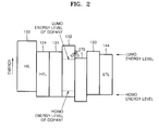
- FIG. 2 is a representation of energy levels of each material layer forming the white OLED of FIG. 1 ;
- FIG. 3 is a graph of the current efficiency according to a brightness of a white OLED by comparing cases when an electron injection induction layer is included and when an electron injection induction layer is not included in the white OLED;
- FIG. 4 is a graph of a light emitting spectrum of a white OLED by comparing cases when an electron injection induction layer is included and when an electron injection induction layer is not included in the white OLED.
- first,” “second,” and the like, “primary,” “secondary,” and the like, as used herein do not denote any order, quantity, or importance, but rather are used to distinguish one element, region, component, layer, or section from another.
- the terms “front”, “back”, “bottom”, and/or “top” are used herein, unless otherwise noted, merely for convenience of description, and are not limited to any one position or spatial orientation.
- the endpoints of all ranges directed to the same component or property are inclusive of the endpoint and independently combinable, e.g., ranges of “up to about 25 wt. %, or, more specifically, about 5 wt. % to about 20 wt. %,” is inclusive of the endpoints and all intermediate values of the ranges of “about 5 wt. % to about 25 wt. %,” etc.
- the modifier “about” used in connection with a quantity is inclusive of the stated value and has the meaning dictated by the context (e.g., includes the degree of error associated with measurement of the particular quantity).
- FIG. 1 is a cross-sectional view of a white Organic Light Emitting Device (OLED) according to an embodiment of the present invention and FIG. 2 is a representation of energy levels of each material layer forming the white OLED of FIG. 1 .
- OLED Organic Light Emitting Device
- the white OLED according to the current embodiment of the present invention includes an anode 110 and a cathode 150 that are spaced apart from each other, first, second, and third light emitting layers 131 , 132 , 133 that are sequentially stacked between the anode 110 and the cathode 150 , and an electron injection induction layer 170 disposed between the second light emitting layer 132 and the third light emitting layer 133 .
- the anode 110 may be formed on a substrate 100 .
- the substrate 100 may be formed of a transparent glass, quartz, or plastic.
- the anode 110 may be formed by depositing transparent conductive materials on the substrate 100 and by patterning the transparent conductive materials.
- the anode 110 is formed of a material having a high conductivity and work function. More specifically, the anode 110 is formed of a material having a work function of about 4.7 eV or above so as to smoothly inject holes.
- the anode 110 may be formed of, for example, Indium Tin Oxide (ITO), Indium Zinc Oxide (IZO), SnO 2 , or ZnO.
- the cathode 150 is formed of a material having a low work function.
- the cathode 150 may be formed of, for example, a metal, such as aluminum (Al), silver (Ag), magnesium (Mg), Lithium (Li), or Calcium (Ca) or an alloy thereof.
- a metal such as aluminum (Al), silver (Ag), magnesium (Mg), Lithium (Li), or Calcium (Ca) or an alloy thereof.
- the materials for forming the cathode 150 are not limited thereto.
- the first, second, and third light emitting layers 131 , 132 , and 133 are sequentially formed between the anode 110 and the cathode 150 .
- the first light emitting layer 131 may be, for example, a red light emitting layer.
- Such a first light emitting layer 131 may be formed by using, for example, a red dopant in a predetermined host material.
- the first light emitting layer 131 may be formed of a material which can smoothly transport holes toward the third light emitting layer 133 . Accordingly, the first light emitting layer 131 includes a host material having a better hole transporting property than an electron transporting property.
- the host material used for the first light emitting layer 131 may be, for example, a triphenylamine derivative such as N,N′-diphenyl-N,N′-bis(3-methylphenyl)-1,1′-bi-phenyl-4,4′-diamine (TPD) or N,N′-di(naphthalen-1-yl)-N,N′-diphenyl-benzidine (NPB).
- TPD N,N′-diphenyl-N,N′-bis(3-methylphenyl)-1,1′-bi-phenyl-4,4′-diamine
- NPB N,N′-di(naphthalen-1-yl)-N,N′-diphenyl-benzidine
- the first light emitting layer 131 is formed to have a thickness of about 1-20 nm, for example.
- the second light emitting layer 132 may be, for example, a green light emitting layer. Such a second light emitting layer 132 may be formed by using, for example, a green dopant in a predetermined host material. As in the first light emitting layer 131 , the second light emitting layer 132 is formed of a material which can smoothly transport holes toward the third light emitting layer 133 . Accordingly, the second light emitting layer 132 includes a host material having a better hole transporting property than an electron transporting property.
- the host material used for the second light emitting layer 132 may be a triphenylamine derivative (for example, N,N′-diphenyl-N,N′-bis(3-methylphenyl)-1,1′-bi-phenyl-4,4′-diamine (TPD) or N,N′-di(naphthalen-1-yl)-N,N′-diphenyl-benzidine (NPB)) or a carbazole compound (for example, 4,4-N,N′-dicarbazole-biphenyl (CBP), a CBP derivative, N,N′-dicarbazolyl-3,5-benzene (mCP), or a mCP derivative).
- TPD N,N′-diphenyl-N,N′-bis(3-methylphenyl)-1,1′-bi-phenyl-4,4′-diamine
- NBP N,N′-di(naphthalen-1-yl)-N,N′-diphen
- the third light emitting layer 133 may be, for example, a blue light emitting layer. Such a third light emitting layer 133 may be formed by using, for example, a blue dopant in a predetermined host material.
- the third light emitting layer 133 uses some of the electrons injected from the cathode 150 during light emitting and transports remaining electrons toward the first and second light emitting layers 131 and 132 . Accordingly, the third light emitting layer 133 may include a fluorescent host material having an excellent hole transporting property and electron transporting property or a phosphorescent host material having a better electron transporting property than a hole transporting property.
- the host material used for the third light emitting layer 133 may be, for example, an anthracene derivative, a pyrene derivative, a perylene derivative, Alq3, a carbazole compound (for example, 4,4-N,N′-dicarbazole-biphenyl (CBP), a CBP derivative, N,N′-dicarbazolyl-3,5-benzene (mCP), or a mCP derivative), phenyloxazole (ZnPBO), or phenylthiazole (ZnPBT).
- CBP 4,4-N,N′-dicarbazole-biphenyl
- mCP N,N′-dicarbazolyl-3,5-benzene
- ZnPBO phenyloxazole
- ZnPBT phenylthiazole
- the third light emitting layer 133 is formed to have a thickness of about 1-20 nm, for example.
- the electron injection induction layer 170 is disposed between the second light emitting layer 132 and the third light emitting layer 133 .
- the electron injection induction layer 170 induces electrons to flow into the second light emitting layer 132 from the third light emitting layer 133 , thereby controlling the intensity of light from the first and second light emitting layers 131 and 132 .
- the electron injection induction layer 170 not only transports the holes toward the third light emitting layer 133 from the first and second light emitting layers 131 and 132 but also injects electrons into a Lowest Occupied Molecular Orbital (LUMO) energy level of the dopant existing in the second light emitting layer 132 , thereby transporting the electrons injected from the third light emitting layer 133 to the second light emitting layer 132 .
- the electron injection induction layer 170 may be formed of a material with the LUMO energy level that is similar to that of the dopant existing in the second light emitting layer 132 .
- the difference between the LUMO energy level of the electron injection induction layer 170 and the LUMO energy level of the dopant existing in the second light emitting layer 132 may be about 0.4 eV or below.
- Such an electron injection induction layer 170 may have an excellent hole transporting property and electron transporting property.
- the electron injection induction layer 170 may be formed of, for example, a carbazole compound such as 4,4-N,N′-dicarbazole-biphenyl (CBP), a CBP derivative, N,N′-dicarbazolyl-3,5-benzene (mCP), or a mCP derivative.
- CBP 4,4-N,N′-dicarbazole-biphenyl
- mCP N,N′-dicarbazolyl-3,5-benzene
- the material for forming the electron injection induction layer 170 is not limited thereto.
- the electron injection induction layer 170 is formed to have a thickness of about 1-10 nm, for example.
- a Hole Transporting Layer (HTL) 124 may be disposed between the anode 110 and the first light emitting layer 131 for easily transporting the hole toward the first light emitting layer 131 .
- the HTL 124 may be formed of, for example, a triphenylamine derivative having high hole mobility and excellent stability such as N,N′-diphenyl-N,N′-bis(3-methylphenyl)-1,1′-bi-phenyl-4,4′-diamine (TPD) or N,N′-di(naphthalen-1-yl)-N,N′-diphenyl-benzidine (NPB).
- TPD N,N′-diphenyl-N,N′-bis(3-methylphenyl)-1,1′-bi-phenyl-4,4′-diamine
- NPB N,N′-di(naphthalen-1-yl)-N,N′-diphenyl-benzidine
- the HTL 124 is formed to have a thickness of about 10 nm or above, for example.
- a Hole Injection Layer (HIL) 122 may be further disposed between the anode 110 and the HTL 124 for easily injecting the hole.
- the HIL 122 may be formed of, for example, a triphenylamine derivative including 4,4′,4′′-tris(3-methylphenylphenylamino)triphenylamine (MTDATA), copper phthalocyanine (CuPc), or poly(3,4-ethylenedioxythiphene, polystyrene sulfonated (PEDOT/PSS).
- MTDATA 4,4′,4′′-tris(3-methylphenylphenylamino)triphenylamine
- CuPc copper phthalocyanine
- PEDOT/PSS poly(3,4-ethylenedioxythiphene, polystyrene sulfonated
- the materials for forming the HIL 122 are not limited thereto
- An Electron Transporting Layer (ETL) 144 may be further disposed between the cathode 150 and the third light emitting layer 133 for easily transporting the electron toward the third light emitting layer 133 .
- the ETL 144 may be formed of, for example, an aryl compound such as oxadiazole, triazole, phenanthroline, benzoxazole, or benzthiazole. However, the material for forming the ETL 144 is not limited thereto.
- an Electron Injection Layer (EIL) 142 may be further disposed between the cathode 150 and the ETL 144 for easily injecting the electrons.
- the EIL 142 may be formed of, for example, Lithium Fluoride (LIF) or Lithium Quinolate (LiQ). However, the material for forming the EIL 142 is not limited thereto.
- the electron injection induction layer 170 is disposed between the second light emitting layer 132 and the third light emitting layer 133 , thereby controlling the intensity of light from the first and second light emitting layers 131 and 132 .
- FIG. 3 is a graph of current efficiency according to a brightness of the white OLED by comparing cases when an electron injection induction layer 170 is included and when an electron injection induction layer is not included in the white OLED. Referring to FIG. 3 , current efficiency is greatly improved in the white OLED including the electron injection induction layer 170 , compared with that of the white OLED without the electron injection induction layer 170 .
- FIG. 4 is a graph of a light emitting spectrum of the white OLED by comparing cases when an electron injection induction layer 170 is included and when an electron injection induction layer is not included in the white OLED. Referring to FIG. 4 , only blue light is observed in the white OLED without the electron injection induction layer 170 , whereas blue, red, and green lights are observed in the white OLED including the electron injection induction layer 170 .
- a white Organic Light Emitting Device includes an electron injection induction layer between second and third light emitting layers to induce electrons to flow toward first and second light emitting layers so that light emitting efficiency is improved and stable colors are realized.
Abstract
Description
Claims (21)
Applications Claiming Priority (2)
| Application Number | Priority Date | Filing Date | Title |
|---|---|---|---|
| KR10-2008-0020083 | 2008-03-04 | ||
| KR1020080020083A KR101453874B1 (en) | 2008-03-04 | 2008-03-04 | White organic light emitting device |
Publications (2)
| Publication Number | Publication Date |
|---|---|
| US20090226757A1 US20090226757A1 (en) | 2009-09-10 |
| US8119258B2 true US8119258B2 (en) | 2012-02-21 |
Family
ID=41053927
Family Applications (1)
| Application Number | Title | Priority Date | Filing Date |
|---|---|---|---|
| US12/213,356 Active 2030-10-31 US8119258B2 (en) | 2008-03-04 | 2008-06-18 | White organic light emitting device (OLED) |
Country Status (2)
| Country | Link |
|---|---|
| US (1) | US8119258B2 (en) |
| KR (1) | KR101453874B1 (en) |
Cited By (2)
| Publication number | Priority date | Publication date | Assignee | Title |
|---|---|---|---|---|
| US20110291817A1 (en) * | 2009-05-26 | 2011-12-01 | Yamaha Corporation | AV Equipment Control Device |
| US20140151668A1 (en) * | 2009-01-13 | 2014-06-05 | Samsung Display Co., Ltd. | Organic light emitting diode and method of manufacturing the same |
Families Citing this family (16)
| Publication number | Priority date | Publication date | Assignee | Title |
|---|---|---|---|---|
| KR101135541B1 (en) | 2010-04-01 | 2012-04-13 | 삼성모바일디스플레이주식회사 | Organic light emitting diode device |
| US9562136B2 (en) | 2011-07-04 | 2017-02-07 | Cambridge Display Technology, Ltd. | Polymers, monomers and methods of forming polymers |
| KR101909775B1 (en) | 2012-04-20 | 2018-10-18 | 가부시키가이샤 한도오따이 에네루기 켄큐쇼 | Light-emitting element, light-emitting device, electronic appliance, and lighting device |
| CN102694131B (en) * | 2012-06-04 | 2015-06-03 | 京东方科技集团股份有限公司 | Organic light-emitting device, manufacturing method thereof and display device |
| US9203045B2 (en) | 2012-11-29 | 2015-12-01 | Semiconductor Energy Laboratory Co., Ltd. | Light-emitting element, light-emitting device, electronic device, and lighting device |
| CN104051647A (en) * | 2013-03-15 | 2014-09-17 | 海洋王照明科技股份有限公司 | Organic electroluminescent device and preparation method thereof |
| KR102230139B1 (en) | 2013-05-17 | 2021-03-18 | 가부시키가이샤 한도오따이 에네루기 켄큐쇼 | Light-emitting element, lighting device, light-emitting device, and electronic device |
| KR102016564B1 (en) * | 2013-07-19 | 2019-09-02 | 엘지디스플레이 주식회사 | Organic light emitting diode device and method for manufacturing of the same |
| CN103715360B (en) * | 2013-12-23 | 2015-01-07 | 京东方科技集团股份有限公司 | Organic electroluminescent device and display device |
| KR101674250B1 (en) * | 2014-02-11 | 2016-11-08 | 단국대학교 산학협력단 | Highly Efficient White OLED |
| KR102145636B1 (en) * | 2014-04-01 | 2020-08-18 | 경희대학교 산학협력단 | Method for manufacturing organic light emitting device and organic light emitting device using the same |
| CN105742310A (en) * | 2014-12-10 | 2016-07-06 | 昆山工研院新型平板显示技术中心有限公司 | Double-layer pixel light-emitting device |
| WO2017011450A1 (en) * | 2015-07-15 | 2017-01-19 | The University Of Florida Research Foundation, Inc. | Conformal conductive scaffolds and methods of using conformal conductive scaffolds |
| KR102523973B1 (en) * | 2016-02-18 | 2023-04-20 | 삼성전자주식회사 | Method of fabricating white organic light emitting device using electrospraying |
| CN105895820B (en) * | 2016-06-21 | 2019-01-22 | 武汉华星光电技术有限公司 | Organic luminescent device and its display |
| JP7015089B2 (en) * | 2016-09-30 | 2022-02-02 | 京東方科技集團股▲ふん▼有限公司 | An organic light emitting diode, a display panel and a display device provided with the organic light emitting diode, and a method for manufacturing the organic light emitting diode. |
Citations (8)
| Publication number | Priority date | Publication date | Assignee | Title |
|---|---|---|---|---|
| US20030068528A1 (en) * | 2001-08-29 | 2003-04-10 | Thompson Mark E. | Organic light emitting devices having carrier blocking layers comprising metal complexes |
| US6831406B1 (en) * | 1999-05-25 | 2004-12-14 | Matsushita Electric Industrial Co., Ltd. | Electroluminescent device having a very thin emission layer |
| US20060227079A1 (en) * | 2003-08-22 | 2006-10-12 | Mitsuhiro Kashiwabara | Organic el device and display |
| US20060231843A1 (en) * | 2002-05-24 | 2006-10-19 | Dashan Qin | Phosphorescent light-emitting component comprising organic layers |
| US20060279203A1 (en) * | 2005-06-01 | 2006-12-14 | Stephen Forrest | Fluorescent filtered electrophosphorescence |
| EP1786242A1 (en) * | 2004-08-05 | 2007-05-16 | Konica Minolta Holdings, Inc. | Organic electroluminescence device, display apparatus and lighting apparatus |
| US20080258606A1 (en) * | 2004-10-08 | 2008-10-23 | Cambridge Display Technology Limited | Light Emitting Device |
| US20080284318A1 (en) * | 2007-05-17 | 2008-11-20 | Deaton Joseph C | Hybrid fluorescent/phosphorescent oleds |
Family Cites Families (1)
| Publication number | Priority date | Publication date | Assignee | Title |
|---|---|---|---|---|
| KR100495594B1 (en) * | 2003-05-23 | 2005-06-14 | 주식회사 비스톰 | White organic light emitting device using three emissive layer |
-
2008
- 2008-03-04 KR KR1020080020083A patent/KR101453874B1/en active IP Right Grant
- 2008-06-18 US US12/213,356 patent/US8119258B2/en active Active
Patent Citations (8)
| Publication number | Priority date | Publication date | Assignee | Title |
|---|---|---|---|---|
| US6831406B1 (en) * | 1999-05-25 | 2004-12-14 | Matsushita Electric Industrial Co., Ltd. | Electroluminescent device having a very thin emission layer |
| US20030068528A1 (en) * | 2001-08-29 | 2003-04-10 | Thompson Mark E. | Organic light emitting devices having carrier blocking layers comprising metal complexes |
| US20060231843A1 (en) * | 2002-05-24 | 2006-10-19 | Dashan Qin | Phosphorescent light-emitting component comprising organic layers |
| US20060227079A1 (en) * | 2003-08-22 | 2006-10-12 | Mitsuhiro Kashiwabara | Organic el device and display |
| EP1786242A1 (en) * | 2004-08-05 | 2007-05-16 | Konica Minolta Holdings, Inc. | Organic electroluminescence device, display apparatus and lighting apparatus |
| US20080258606A1 (en) * | 2004-10-08 | 2008-10-23 | Cambridge Display Technology Limited | Light Emitting Device |
| US20060279203A1 (en) * | 2005-06-01 | 2006-12-14 | Stephen Forrest | Fluorescent filtered electrophosphorescence |
| US20080284318A1 (en) * | 2007-05-17 | 2008-11-20 | Deaton Joseph C | Hybrid fluorescent/phosphorescent oleds |
Cited By (3)
| Publication number | Priority date | Publication date | Assignee | Title |
|---|---|---|---|---|
| US20140151668A1 (en) * | 2009-01-13 | 2014-06-05 | Samsung Display Co., Ltd. | Organic light emitting diode and method of manufacturing the same |
| US9196857B2 (en) * | 2009-01-13 | 2015-11-24 | Samsung Display Co., Ltd. | Organic light emitting diode and method of manufacturing the same |
| US20110291817A1 (en) * | 2009-05-26 | 2011-12-01 | Yamaha Corporation | AV Equipment Control Device |
Also Published As
| Publication number | Publication date |
|---|---|
| US20090226757A1 (en) | 2009-09-10 |
| KR101453874B1 (en) | 2014-10-21 |
| KR20090095022A (en) | 2009-09-09 |
Similar Documents
| Publication | Publication Date | Title |
|---|---|---|
| US8119258B2 (en) | White organic light emitting device (OLED) | |
| US7906900B2 (en) | White organic light emitting device | |
| Karzazi | Organic light emitting diodes: devices and applications | |
| TWI478624B (en) | Organic electroluminescent elements | |
| US11711933B2 (en) | OLED device structures | |
| JP5476061B2 (en) | Organic electroluminescence device and method for manufacturing the same | |
| JP4895742B2 (en) | White organic electroluminescence device | |
| JP6089280B2 (en) | Organic electroluminescence device | |
| US8482017B2 (en) | Organic light emitting diode device | |
| JP4966176B2 (en) | Organic electroluminescence device | |
| Zhang et al. | High efficiency fluorescent white organic light-emitting diodes with red, green and blue separately monochromatic emission layers | |
| JP2010109364A (en) | Organic light-emitting diode device and manufacturing method thereof | |
| JP2011054668A (en) | Organic electroluminescence device | |
| JP2006048946A (en) | Organic functional element, organic el element, organic semiconductor element, organic tft element, and manufacturing method for them | |
| JP2001155862A (en) | Light emitting element and method of manufacturing the same | |
| TW201136446A (en) | Organic light-emitting diode with high color rendering | |
| JP5109054B2 (en) | Organic electroluminescence device | |
| WO2015192591A1 (en) | Organic electroluminescence device and organic electroluminescence display apparatus | |
| KR100760901B1 (en) | The White Organic Light Emitting Device | |
| US20110303902A1 (en) | Organic light-emitting diode with high color rendering | |
| JP2014127303A (en) | Method of manufacturing organic el device | |
| KR20050063659A (en) | White organic light emitting device | |
| JP2003282267A (en) | Light emitting device | |
| JP2004031211A (en) | Organic electroluminescent element | |
| TW201515295A (en) | Top emitting blue OLED and fabrication method thereof |
Legal Events
| Date | Code | Title | Description |
|---|---|---|---|
| AS | Assignment |
Owner name: SAMSUNG ELECTRONICS CO., LTD., A CORP. OF THE REPU Free format text: ASSIGNMENT OF ASSIGNORS INTEREST;ASSIGNORS:SONG, JUNG-BAE;LEE, SUNG-HUN;KIM, SANG-YEOL;AND OTHERS;REEL/FRAME:021355/0262;SIGNING DATES FROM 20080611 TO 20080612 Owner name: SAMSUNG SDI CO., LTD., A CORP. OF THE REPUBLIC OF Free format text: ASSIGNMENT OF ASSIGNORS INTEREST;ASSIGNORS:SONG, JUNG-BAE;LEE, SUNG-HUN;KIM, SANG-YEOL;AND OTHERS;REEL/FRAME:021355/0262;SIGNING DATES FROM 20080611 TO 20080612 Owner name: SAMSUNG ELECTRONICS CO., LTD., A CORP. OF THE REPU Free format text: ASSIGNMENT OF ASSIGNORS INTEREST;ASSIGNORS:SONG, JUNG-BAE;LEE, SUNG-HUN;KIM, SANG-YEOL;AND OTHERS;SIGNING DATES FROM 20080611 TO 20080612;REEL/FRAME:021355/0262 Owner name: SAMSUNG SDI CO., LTD., A CORP. OF THE REPUBLIC OF Free format text: ASSIGNMENT OF ASSIGNORS INTEREST;ASSIGNORS:SONG, JUNG-BAE;LEE, SUNG-HUN;KIM, SANG-YEOL;AND OTHERS;SIGNING DATES FROM 20080611 TO 20080612;REEL/FRAME:021355/0262 |
|
| AS | Assignment |
Owner name: SAMSUNG MOBILE DISPLAY CO., LTD., KOREA, REPUBLIC Free format text: ASSIGNMENT OF ASSIGNORS INTEREST;ASSIGNOR:SAMSUNG SDI CO., LTD.;REEL/FRAME:023620/0798 Effective date: 20091113 |
|
| STCF | Information on status: patent grant |
Free format text: PATENTED CASE |
|
| AS | Assignment |
Owner name: SAMSUNG DISPLAY CO., LTD., KOREA, REPUBLIC OF Free format text: MERGER;ASSIGNOR:SAMSUNG MOBILE DISPLAY CO., LTD.;REEL/FRAME:029241/0599 Effective date: 20120702 |
|
| AS | Assignment |
Owner name: SAMSUNG DISPLAY CO., LTD., KOREA, REPUBLIC OF Free format text: ASSIGNMENT OF ASSIGNORS INTEREST;ASSIGNOR:SAMSUNG ELECTRONICS CO., LTD.;REEL/FRAME:029093/0177 Effective date: 20120904 |
|
| FEPP | Fee payment procedure |
Free format text: PAYOR NUMBER ASSIGNED (ORIGINAL EVENT CODE: ASPN); ENTITY STATUS OF PATENT OWNER: LARGE ENTITY |
|
| FPAY | Fee payment |
Year of fee payment: 4 |
|
| MAFP | Maintenance fee payment |
Free format text: PAYMENT OF MAINTENANCE FEE, 8TH YEAR, LARGE ENTITY (ORIGINAL EVENT CODE: M1552); ENTITY STATUS OF PATENT OWNER: LARGE ENTITY Year of fee payment: 8 |
|
| MAFP | Maintenance fee payment |
Free format text: PAYMENT OF MAINTENANCE FEE, 12TH YEAR, LARGE ENTITY (ORIGINAL EVENT CODE: M1553); ENTITY STATUS OF PATENT OWNER: LARGE ENTITY Year of fee payment: 12 |