US8098847B2 - Muting circuit - Google Patents
Muting circuit Download PDFInfo
- Publication number
- US8098847B2 US8098847B2 US11/858,848 US85884807A US8098847B2 US 8098847 B2 US8098847 B2 US 8098847B2 US 85884807 A US85884807 A US 85884807A US 8098847 B2 US8098847 B2 US 8098847B2
- Authority
- US
- United States
- Prior art keywords
- muting
- operational amplifier
- input
- output
- signal
- Prior art date
- Legal status (The legal status is an assumption and is not a legal conclusion. Google has not performed a legal analysis and makes no representation as to the accuracy of the status listed.)
- Active, expires
Links
Images


Classifications
-
- H—ELECTRICITY
- H03—ELECTRONIC CIRCUITRY
- H03G—CONTROL OF AMPLIFICATION
- H03G3/00—Gain control in amplifiers or frequency changers
- H03G3/20—Automatic control
- H03G3/30—Automatic control in amplifiers having semiconductor devices
- H03G3/34—Muting amplifier when no signal is present
- H03G3/344—Muting responsive to the amount of noise (noise squelch)
-
- G—PHYSICS
- G11—INFORMATION STORAGE
- G11B—INFORMATION STORAGE BASED ON RELATIVE MOVEMENT BETWEEN RECORD CARRIER AND TRANSDUCER
- G11B20/00—Signal processing not specific to the method of recording or reproducing; Circuits therefor
- G11B20/24—Signal processing not specific to the method of recording or reproducing; Circuits therefor for reducing noise
-
- H—ELECTRICITY
- H03—ELECTRONIC CIRCUITRY
- H03K—PULSE TECHNIQUE
- H03K17/00—Electronic switching or gating, i.e. not by contact-making and –breaking
- H03K17/26—Modifications for temporary blocking after receipt of control pulses
-
- H—ELECTRICITY
- H04—ELECTRIC COMMUNICATION TECHNIQUE
- H04R—LOUDSPEAKERS, MICROPHONES, GRAMOPHONE PICK-UPS OR LIKE ACOUSTIC ELECTROMECHANICAL TRANSDUCERS; ELECTRIC HEARING AIDS; PUBLIC ADDRESS SYSTEMS
- H04R3/00—Circuits for transducers
- H04R3/002—Damping circuit arrangements for transducers, e.g. motional feedback circuits
Definitions
- the present invention relates to a muting circuit.
- An electronic volume that electronically controls the volume of speakers is typically provided with a muting circuit that produces no-sound condition (mute) by temporarily cutting off an audio signal when the noise superimposed upon the audio signal is detected or when a mute button is pressed.
- the pitch and the volume of an audio signal are known to have characteristics to be adjusted by frequency control and by amplitude control, respectively.
- a muting circuit executes a process to produce no-sound condition (hereinafter, referred to as a muting process) by fixing a DC level at a predetermined level to eliminate the amplitude of the audio signal (see FIG. 4 ).
- a muting process As the predetermined DC level, “AC-GND” in an electronic volume is generally employed.
- the AC-GND means a GND applied for an AC signal that indicates a constant DC level as the amplitude center of an AC signal waveform.
- FIG. 5 is a schematic illustrating the configuration of an electronic volume 10 equipped with a conventional muting circuit 30 .
- the electronic volume 10 is composed mainly of an attenuation amount control circuit 20 that controls the attenuation amount of an AC input signal IN (audio signal) for volume control, and a muting circuit 30 , that is equipped with analogue switches SW 1 and SW 2 that are switched on and off complimentarily by the electronic control of a microcomputer (not shown), that executes the muting process for the AC input signal IN after attenuation amount control (see, e.g., Japanese Patent Application Laid-Open Publication No. 1999-327579).
- the muting circuit 30 In normal state where muting process is not executed, the muting circuit 30 outputs the attenuation amount-controlled AC input signal IN as is as an AC output signal OUT by switching the analogue switches SW 1 on and SW 2 off.
- the amplitude center of the AC input signal IN is to indicate a constant DC level Va.
- the muting circuit 30 outputs an AC-GND level Vb by switching the analogue switches SW 1 off and SW 2 on (see sections a and b of FIG. 6 ). Consequently, no-sound condition can be produced since the DC level of the AC output signal OUT is fixed at the AC-GND level Vb.
- an AC input signal IN without muting process contains a DC offset Vx, that is a difference voltage between the AC-GND level Vb, due to the internal circuit characteristics of the electronic volume 10 and/or due to the manufacturing variation of ICs that compose the attenuation amount control circuit 20 .
- the DC voltage of an AC output signal OUT is fluctuated by the DC offset Vx when the analogue switches SW 1 and SW 2 are switched-over between on and off, and noise is generated by such DC voltage fluctuations.
- a muting circuit comprises: a DC offset eliminating unit including an HPF (High Pass Filter) constituted by a first operational amplifier to eliminate a DC offset component of an AC input signal, the DC offset eliminating unit being configured to output an output signal obtained by eliminating the DC offset component of the AC input signal; a muting signal generating unit including a second operational amplifier configured to generate a second DC offset identical in level to a first DC offset at the first operational amplifier, the muting signal generating unit being configured to output a muting signal indicative of the second DC offset by fixing input to the second operational amplifier at a predetermined DC level; and a selecting unit configured to select and output the output signal when muting is not executed, and to select and output the muting signal when muting is executed.
- HPF High Pass Filter
- FIG. 1 is a schematic illustrating the configuration of an audio signal processing system according to an embodiment of the present invention
- FIG. 2 is a schematic illustrating the configuration of a muting circuit according to an embodiment of the present invention
- FIG. 3 is a schematic illustrating the principal state transition to explain the operation of a muting circuit according to an embodiment of the present invention
- FIG. 4 is a schematic illustrating the mechanism of a muting process
- FIG. 5 is a schematic illustrating the mechanism of an electronic volume employing a conventional muting circuit
- FIG. 6 is a schematic illustrating the principal state transition to explain the operation (problem) of a conventional muting circuit.
- FIG. 1 is a schematic illustrating the configuration of an audio signal processing system according to an embodiment of the present invention.
- sound signals from various sound sources such as a television, an AM/FM radio, a VTR (Video Tape Recorder), optical discs like a CD and a DVD, AUX (AUXiliary), etc. can be considered.
- VTR Video Tape Recorder
- AUX AUXiliary
- the audio signal processing system is composed of an acoustic DSP (Digital Signal Processor) 100 that executes a digital signal process, such as equalization and sound field correction, on digital audio signals from various sound sources, an electronic volume 200 that controls sound volume by the attenuation amount control of an analogue audio signal, that is D/A converted from the output of the DSP 100 , a power amplifier 300 that drives a speaker 500 to output an analogue audio signal after volume-control by the electronic volume 200 , and a microcomputer 400 for the integrated control of the entire system.
- acoustic DSP Digital Signal Processor
- an electronic volume 200 that controls sound volume by the attenuation amount control of an analogue audio signal, that is D/A converted from the output of the DSP 100
- a power amplifier 300 that drives a speaker 500 to output an analogue audio signal after volume-control by the electronic volume 200
- a microcomputer 400 for the integrated control of the entire system.
- the electronic volume 200 is equipped with an attenuation amount control unit 210 and a muting circuit 220 , that are to be controlled by the microcomputer 400 , and is a single chip of analogue/digital system-on-a-chip LSI, that is independent from the DSP 100 .
- the attenuation amount control unit 210 controls the attenuation amount of an AC input signal IN (analogue audio signal) for the purpose of sound volume control, that is a primary function of the electronic volume 200 .
- an AC input signal IN analogue audio signal
- attenuation amount by the negative-feedback amplifier is controlled based on the value of combined feedback resistance by appropriately switching on and off the multiple analogue switches according to the sound volume indicated by the microcomputer 400 .
- the muting circuit 220 is a circuit to output an AC output signal that is obtained by muting an AC input signal IN′ (AC input signal IN after attenuation amount control) by fixing its amplitude level at a DC level (for example, AC-GND level).
- the electronic volume 200 may be disposed before the DSP 100 for the system configuration to receive an analogue audio signal. It is also possible to integrate the function(s) of the electronic volume 200 (for example, attenuation amount control function), other than the muting circuit 220 , as a part of the functions of the DSP 100 .
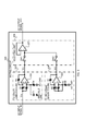
- FIG. 3 is a schematic illustrating the principal state transition to explain the operation of a muting circuit 220 .
- the muting circuit 220 is equipped with a DC offset eliminating unit 221 , a muting signal generating unit 224 , analogue switches SW 1 , SW 2 , and a voltage follower 227 .
- the DC offset eliminating unit 221 is a circuit to eliminate DC offset components included in an AC input signal IN′, that are generated due to the internal circuit (e.g., the attenuation amount control unit 210 ) characteristics of the electronic volume 200 and/or due to the manufacturing variation of ICs, by routing the DC offset components through an HPF (High Pass Filter) constituted by an operational amplifier 222 (a “first operational amplifier” according to the present invention).
- HPF High Pass Filter
- a first feedback resistance R 3 is disposed in the negative-feedback path of the operational amplifier 222 ; a first input resistance R 1 and a second input resistance R 2 are arranged at the inverting input side and the non-inverting input side of the operational amplifier 222 , respectively; the AC input signal IN′ is input in common to the inverting input and non-inverting input of the operational amplifier 222 through the first and second input resistances R 1 and R 2 , respectively; and a DC cut capacitor C 1 is disposed between the non-inverting input of the operational amplifier 222 and an AC-GND or an analogue GND in parallel with a first ground resistance R 4 .
- the DC offset eliminating unit 221 constitutes the HPF.
- a DC offset Vy (a “first DC offset” according to the present invention) specific to the operational amplifier 222 will be included in the AC input signal IN′ since the operational amplifier 222 is employed in the DC offset eliminating unit 221 .
- the DC offset Vy specific to the operational amplifier 222 is indicated as the DC voltage of an output voltage Vc referring to an AC-GND level.
- a muting signal generating unit 224 is a circuit constituted by an operational amplifier 225 (a “second operational amplifier” according to the present invention) that generates a DC offset Vy′ (a “second DC offset” according to the present invention) identical to the level of a DC offset Vy specific to the operational amplifier 222 , and outputs a muting signal Vd that indicates the DC offset Vy′ by fixing an input to the operational amplifier 225 at the AC-GND level that is common to the operational amplifier 222 .
- the DC offsets Vy and Vy′ can be set at an identical level by employing the operational amplifiers 222 and 225 produced from an identical wafer and thus with an identical performance.
- the operational amplifier 225 can set DC offsets Vy and Vy′ more accurately at an identical level. Its concrete configuration is as follows: a second feedback resistance R 7 identical to the first feedback resistance R 3 is disposed in the negative-feedback path of the operational amplifier 225 ; a third input resistance R 5 identical to the first input resistance R 1 and a fourth input resistance R 6 identical to the second input resistance R 2 are arranged on the inverting input side and on the non-inverting input side of the operational amplifier 225 , respectively; and the third and fourth input resistances R 5 and R 6 are connected in common to the AC-GND, that is common to the operational amplifier 222 , through a second ground resistance R 8 identical to the first ground resistance R 4 .
- a selecting unit 226 is a circuit that receives an AC input signal IN′ (hereinafter, referred to as an AC input signal Vc) after DC offset elimination, output by the DC offset eliminating unit 221 , and a muting signal Vd output by the muting signal generating unit 224 , and then selects the AC input signal Vc to output as an AC output signal OUT in a normal state without muting, or selects the muting signal Vd to output as an AC output signal OUT in a state muting is necessary.
- the selecting unit 226 is provided with the analogue switches SW 1 and SW 2 with identical characteristics, that are complementarily switched on and off by the electronic control by the microcomputer 400 , to select and to output an AC input signal Vc or a muting signal Vd.
- the analogue switch SW 1 is disposed between the output of the operation amplifier 222 and the non-inverting input of the voltage follower 227 .
- the analogue switch SW 1 is switched on, and an AC input signal Vc is input to the non-inverting input of the voltage follower 227 .
- the analogue switch SW 1 is switched off, and the input of the AC input signal Vc to the non-inverting input of the voltage follower 227 is shut off.
- the analogue switch SW 2 is disposed between the output of the operation amplifier 225 and the non-inverting input of the voltage follower 227 .
- the analogue switch SW 2 is switched on, and a muting signal Vd is input to the non-inverting input of the voltage follower 227 .
- the analogue switch SW 2 is switched off, and the input of the muting signal Vd to the non-inverting input of the voltage follower 227 is shut off.
- analogue switch SW 1 is on and the analogue switch SW 2 is off, a muting process is not executed, and an AC output signal OUT from the muting circuit 220 , that is output through the voltage follower 227 , is identical to an AC input signal Vc with a DC level of the DC offset level Vy specific to the operational amplifier 222 (sections a and b of FIG. 3 ).
- analogue switch SW 1 is off and the analogue switch SW 2 is on, a muting process is executed, and an AC output signal OUT from the muting circuit 220 , that is output through the voltage follower 227 , is a muting signal Vd that indicates a DC offset Vy′ identical to the level of the DC offset Vy specific to the operational amplifier 222 (sections a and b of FIG. 3 ).
- the operational amplifiers 222 and 225 are produced from an identical wafer and thus have identical performances, and as their peripheral circuit designs and composing elements are also identical, the DC offsets Vy and Vy′ can be regarded as virtually identical. Therefore, as the level of the AC output signal OUT from the muting circuit 220 can be regarded to be constant without fluctuations (section c of FIG. 3 ) at the timing of the switching over of the analogue switches SW 1 and SW 2 between on and off, i.e., at the timing of the start or the end of muting, it is possible to reduce not only noises out of the audible frequency range, as has been done, but also those within the audible frequency range.
Landscapes
- Engineering & Computer Science (AREA)
- Signal Processing (AREA)
- Physics & Mathematics (AREA)
- Acoustics & Sound (AREA)
- Amplifiers (AREA)
- Circuit For Audible Band Transducer (AREA)
Abstract
Description
Claims (4)
Applications Claiming Priority (2)
| Application Number | Priority Date | Filing Date | Title |
|---|---|---|---|
| JP2006256163A JP2008079032A (en) | 2006-09-21 | 2006-09-21 | Mute circuit |
| JP2006-256163 | 2006-09-21 |
Publications (2)
| Publication Number | Publication Date |
|---|---|
| US20080075301A1 US20080075301A1 (en) | 2008-03-27 |
| US8098847B2 true US8098847B2 (en) | 2012-01-17 |
Family
ID=39224989
Family Applications (1)
| Application Number | Title | Priority Date | Filing Date |
|---|---|---|---|
| US11/858,848 Active 2030-11-16 US8098847B2 (en) | 2006-09-21 | 2007-09-20 | Muting circuit |
Country Status (4)
| Country | Link |
|---|---|
| US (1) | US8098847B2 (en) |
| JP (1) | JP2008079032A (en) |
| KR (1) | KR20080027152A (en) |
| CN (1) | CN101150298A (en) |
Families Citing this family (6)
| Publication number | Priority date | Publication date | Assignee | Title |
|---|---|---|---|---|
| JP5189939B2 (en) * | 2008-09-11 | 2013-04-24 | 旭化成エレクトロニクス株式会社 | Variable gain inverting amplifier circuit |
| KR101826036B1 (en) * | 2011-11-07 | 2018-02-07 | 삼성전자주식회사 | Apparatus and method for reducing the dc offset using randomized control pulse |
| CN109765046A (en) * | 2019-03-14 | 2019-05-17 | 克诺尔车辆设备(苏州)有限公司 | A kind of pressure switch detection equipment and calibration method |
| JP7382862B2 (en) * | 2020-03-13 | 2023-11-17 | 株式会社平和 | gaming machine |
| US11228289B1 (en) * | 2020-08-24 | 2022-01-18 | Cirrus Logic, Inc. | Amplifiers |
| CN113285694A (en) * | 2021-05-31 | 2021-08-20 | 杭州雄迈集成电路技术股份有限公司 | Mute circuit of audio codec filter and control method thereof |
Citations (5)
| Publication number | Priority date | Publication date | Assignee | Title |
|---|---|---|---|---|
| JPH11327579A (en) | 1998-05-19 | 1999-11-26 | Fujitsu Ltd | Audio mute circuit |
| KR19990084329A (en) | 1998-05-04 | 1999-12-06 | 윤종용 | Mute Circuit of FM Receiver |
| KR20040014819A (en) | 2002-08-12 | 2004-02-18 | 엘지전자 주식회사 | Mute control circuit for audio amplifier |
| US6734746B1 (en) * | 2001-07-06 | 2004-05-11 | Asahi Kasei Microsystems Co., Ltd. | Mute circuit |
| US20070127742A1 (en) * | 2000-10-25 | 2007-06-07 | National Semiconductor Corporation | Output coupling capacitor free audio power amplifier dynamically configured for speakers and headphones with excellent click and pop performance |
-
2006
- 2006-09-21 JP JP2006256163A patent/JP2008079032A/en active Pending
-
2007
- 2007-07-17 CN CNA2007101368330A patent/CN101150298A/en active Pending
- 2007-09-19 KR KR1020070095290A patent/KR20080027152A/en not_active Ceased
- 2007-09-20 US US11/858,848 patent/US8098847B2/en active Active
Patent Citations (5)
| Publication number | Priority date | Publication date | Assignee | Title |
|---|---|---|---|---|
| KR19990084329A (en) | 1998-05-04 | 1999-12-06 | 윤종용 | Mute Circuit of FM Receiver |
| JPH11327579A (en) | 1998-05-19 | 1999-11-26 | Fujitsu Ltd | Audio mute circuit |
| US20070127742A1 (en) * | 2000-10-25 | 2007-06-07 | National Semiconductor Corporation | Output coupling capacitor free audio power amplifier dynamically configured for speakers and headphones with excellent click and pop performance |
| US6734746B1 (en) * | 2001-07-06 | 2004-05-11 | Asahi Kasei Microsystems Co., Ltd. | Mute circuit |
| KR20040014819A (en) | 2002-08-12 | 2004-02-18 | 엘지전자 주식회사 | Mute control circuit for audio amplifier |
Non-Patent Citations (1)
| Title |
|---|
| KR Intellectual Property Office, Notification of Submission of Opinions dated Dec. 8, 2008, in KR Appln. No. 10-2007-95290. English translation. |
Also Published As
| Publication number | Publication date |
|---|---|
| CN101150298A (en) | 2008-03-26 |
| KR20080027152A (en) | 2008-03-26 |
| US20080075301A1 (en) | 2008-03-27 |
| JP2008079032A (en) | 2008-04-03 |
Similar Documents
| Publication | Publication Date | Title |
|---|---|---|
| US8098847B2 (en) | Muting circuit | |
| US8761408B2 (en) | Signal processing apparatus and signal processing method | |
| US9014397B2 (en) | Signal processing device and signal processing method | |
| US7711128B2 (en) | System, circuit, and amplifier for reducing pop sound | |
| JPH034611A (en) | On-vehicle automatic sound volume adjustment device | |
| US20120163614A1 (en) | Sound signal output device, speaker device, sound output device, and sound signal output method | |
| US10063249B2 (en) | Audio circuit for suppressing DC shock noise | |
| JP3615983B2 (en) | In-vehicle noise control system | |
| JP4662860B2 (en) | Pop noise reduction circuit | |
| US20090046872A1 (en) | Automatic audio level control | |
| WO2021123721A1 (en) | Two-way microphone system using loudspeaker as one of the microphones | |
| JP2009081641A (en) | Unbalance-balance conversion circuit | |
| JP4759015B2 (en) | Constant voltage circuit | |
| JP5032367B2 (en) | Audio signal processing circuit | |
| US20080285760A1 (en) | Audio system for improving a signal to noise ratio | |
| JP6507893B2 (en) | Amplification device and speaker device | |
| JP3638442B2 (en) | Volume circuit | |
| JP2009088831A (en) | Voice output apparatus | |
| EP1786236B1 (en) | Complementary-pair equalizer | |
| JP3929832B2 (en) | Input signal processing circuit | |
| JP2006325262A (en) | Limiter control device and limiter control method | |
| JP2866274B2 (en) | Addition device, game device and audio device provided therewith | |
| JP2005123759A (en) | Output variable circuit for digital to analog converter | |
| JPH07143591A (en) | Audio device | |
| KR19990042768A (en) | How to automatically mute the microphone signal of a song accompaniment video cassette recorder |
Legal Events
| Date | Code | Title | Description |
|---|---|---|---|
| AS | Assignment |
Owner name: SANYO ELECTRIC CO., LTD., JAPAN Free format text: ASSIGNMENT OF ASSIGNORS INTEREST;ASSIGNOR:WATANABE, AKIO;REEL/FRAME:021263/0220 Effective date: 20071001 Owner name: SANYO SEMICONDUCTOR CO., LTD., JAPAN Free format text: ASSIGNMENT OF ASSIGNORS INTEREST;ASSIGNOR:WATANABE, AKIO;REEL/FRAME:021263/0220 Effective date: 20071001 |
|
| AS | Assignment |
Owner name: SEMICONDUCTOR COMPONENTS INDUSTRIES, LLC, ARIZONA Free format text: ASSIGNMENT OF ASSIGNORS INTEREST;ASSIGNOR:SANYO ELECTRIC CO., LTD.;REEL/FRAME:026594/0385 Effective date: 20110101 |
|
| STCF | Information on status: patent grant |
Free format text: PATENTED CASE |
|
| AS | Assignment |
Owner name: SEMICONDUCTOR COMPONENTS INDUSTRIES, LLC, ARIZONA Free format text: CORRECTIVE ASSIGNMENT TO CORRECT THE INCORRECT #12/577882 PREVIOUSLY RECORDED ON REEL 026594 FRAME 0385. ASSIGNOR(S) HEREBY CONFIRMS THE ASSIGNMENT;ASSIGNOR:SANYO ELECTRIC CO., LTD;REEL/FRAME:032836/0342 Effective date: 20110101 |
|
| AS | Assignment |
Owner name: SEMICONDUCTOR COMPONENTS INDUSTRIES, LLC, ARIZONA Free format text: ASSIGNMENT OF ASSIGNORS INTEREST;ASSIGNOR:SANYO SEMICONDUCTOR CO., LTD.;REEL/FRAME:032891/0906 Effective date: 20140509 |
|
| FPAY | Fee payment |
Year of fee payment: 4 |
|
| AS | Assignment |
Owner name: SYSTEM SOLUTIONS CO., LTD., JAPAN Free format text: CHANGE OF NAME;ASSIGNOR:SANYO SEMICONDUCTOR CO., LTD.;REEL/FRAME:037773/0090 Effective date: 20140228 |
|
| AS | Assignment |
Owner name: SEMICONDUCTOR COMPONENTS INDUSTRIES, LLC, ARIZONA Free format text: CORRECTIVE ASSIGNMENT TO CORRECT THE ASSIGNOR NAME PREVIOUSLY RECORDED AT REEL: 032891 FRAME: 0906. ASSIGNOR(S) HEREBY CONFIRMS THE ASSIGNMENT;ASSIGNOR:SYSTEM SOLUTIONS CO., LTD.;REEL/FRAME:037881/0027 Effective date: 20140509 |
|
| AS | Assignment |
Owner name: DEUTSCHE BANK AG NEW YORK BRANCH, NEW YORK Free format text: SECURITY INTEREST;ASSIGNOR:SEMICONDUCTOR COMPONENTS INDUSTRIES, LLC;REEL/FRAME:038620/0087 Effective date: 20160415 |
|
| AS | Assignment |
Owner name: DEUTSCHE BANK AG NEW YORK BRANCH, AS COLLATERAL AG Free format text: CORRECTIVE ASSIGNMENT TO CORRECT THE INCORRECT PATENT NUMBER 5859768 AND TO RECITE COLLATERAL AGENT ROLE OF RECEIVING PARTY IN THE SECURITY INTEREST PREVIOUSLY RECORDED ON REEL 038620 FRAME 0087. ASSIGNOR(S) HEREBY CONFIRMS THE SECURITY INTEREST;ASSIGNOR:SEMICONDUCTOR COMPONENTS INDUSTRIES, LLC;REEL/FRAME:039853/0001 Effective date: 20160415 Owner name: DEUTSCHE BANK AG NEW YORK BRANCH, AS COLLATERAL AGENT, NEW YORK Free format text: CORRECTIVE ASSIGNMENT TO CORRECT THE INCORRECT PATENT NUMBER 5859768 AND TO RECITE COLLATERAL AGENT ROLE OF RECEIVING PARTY IN THE SECURITY INTEREST PREVIOUSLY RECORDED ON REEL 038620 FRAME 0087. ASSIGNOR(S) HEREBY CONFIRMS THE SECURITY INTEREST;ASSIGNOR:SEMICONDUCTOR COMPONENTS INDUSTRIES, LLC;REEL/FRAME:039853/0001 Effective date: 20160415 |
|
| MAFP | Maintenance fee payment |
Free format text: PAYMENT OF MAINTENANCE FEE, 8TH YEAR, LARGE ENTITY (ORIGINAL EVENT CODE: M1552); ENTITY STATUS OF PATENT OWNER: LARGE ENTITY Year of fee payment: 8 |
|
| MAFP | Maintenance fee payment |
Free format text: PAYMENT OF MAINTENANCE FEE, 12TH YEAR, LARGE ENTITY (ORIGINAL EVENT CODE: M1553); ENTITY STATUS OF PATENT OWNER: LARGE ENTITY Year of fee payment: 12 |
|
| AS | Assignment |
Owner name: FAIRCHILD SEMICONDUCTOR CORPORATION, ARIZONA Free format text: RELEASE OF SECURITY INTEREST IN PATENTS RECORDED AT REEL 038620, FRAME 0087;ASSIGNOR:DEUTSCHE BANK AG NEW YORK BRANCH, AS COLLATERAL AGENT;REEL/FRAME:064070/0001 Effective date: 20230622 Owner name: SEMICONDUCTOR COMPONENTS INDUSTRIES, LLC, ARIZONA Free format text: RELEASE OF SECURITY INTEREST IN PATENTS RECORDED AT REEL 038620, FRAME 0087;ASSIGNOR:DEUTSCHE BANK AG NEW YORK BRANCH, AS COLLATERAL AGENT;REEL/FRAME:064070/0001 Effective date: 20230622 |