US8097520B2 - Integration of passive device structures with metal gate layers - Google Patents
Integration of passive device structures with metal gate layers Download PDFInfo
- Publication number
- US8097520B2 US8097520B2 US12/543,544 US54354409A US8097520B2 US 8097520 B2 US8097520 B2 US 8097520B2 US 54354409 A US54354409 A US 54354409A US 8097520 B2 US8097520 B2 US 8097520B2
- Authority
- US
- United States
- Prior art keywords
- layer
- passive device
- semiconductor layer
- metal gate
- contact regions
- Prior art date
- Legal status (The legal status is an assumption and is not a legal conclusion. Google has not performed a legal analysis and makes no representation as to the accuracy of the status listed.)
- Expired - Fee Related, expires
Links
Images


Classifications
-
- H—ELECTRICITY
- H10—SEMICONDUCTOR DEVICES; ELECTRIC SOLID-STATE DEVICES NOT OTHERWISE PROVIDED FOR
- H10D—INORGANIC ELECTRIC SEMICONDUCTOR DEVICES
- H10D1/00—Resistors, capacitors or inductors
- H10D1/40—Resistors
- H10D1/47—Resistors having no potential barriers
-
- H—ELECTRICITY
- H10—SEMICONDUCTOR DEVICES; ELECTRIC SOLID-STATE DEVICES NOT OTHERWISE PROVIDED FOR
- H10D—INORGANIC ELECTRIC SEMICONDUCTOR DEVICES
- H10D84/00—Integrated devices formed in or on semiconductor substrates that comprise only semiconducting layers, e.g. on Si wafers or on GaAs-on-Si wafers
- H10D84/80—Integrated devices formed in or on semiconductor substrates that comprise only semiconducting layers, e.g. on Si wafers or on GaAs-on-Si wafers characterised by the integration of at least one component covered by groups H10D12/00 or H10D30/00, e.g. integration of IGFETs
- H10D84/811—Combinations of field-effect devices and one or more diodes, capacitors or resistors
- H10D84/817—Combinations of field-effect devices and resistors only
-
- H—ELECTRICITY
- H10—SEMICONDUCTOR DEVICES; ELECTRIC SOLID-STATE DEVICES NOT OTHERWISE PROVIDED FOR
- H10D—INORGANIC ELECTRIC SEMICONDUCTOR DEVICES
- H10D1/00—Resistors, capacitors or inductors
- H10D1/40—Resistors
- H10D1/47—Resistors having no potential barriers
- H10D1/474—Resistors having no potential barriers comprising refractory metals, transition metals, noble metals, metal compounds or metal alloys, e.g. silicides
Definitions
- the present invention relates generally to semiconductor device manufacturing and, more particularly, to improved integration of passive device structures with metal gate layers.
- CMOS complementary metal oxide semiconductor
- polysilicon is typically used as the standard gate material.
- the technology of fabricating CMOS devices using polysilicon gates has been in a constant state of development, and is now widely used in the semiconductor industry.
- One advantage of using polysilicon gates is that they can sustain high temperatures.
- polysilicon gates commonly used in CMOS devices are becoming a gating factor in chip performance for channel lengths of 0.1 micron and below.
- Another problem with polysilicon gates is that the dopant material in the polysilicon gate (e.g., boron) can easily diffuse through the thin gate dielectric causing further degradation of the device performance.
- one proposed way of improving the performance of sub-micron transistors is to use metal gates in place of conventional polysilicon gates, particularly with the advent of high-k gate dielectric materials.
- transistor devices In addition to transistor devices, other types of devices are also formed on integrated circuits. For example, certain passive device structures such as resistors and eFUSEs are formed above the substrate level. In particular, where such devices are integrated with metal gate technology, a silicon layer is formed on top of the metal gate layer (used in forming the metal gates in the transistor region). Thus, while the metal gate layer located in the transistor or active device regions is patterned according to a desired gate structure, the other portions of the metal gate layer residing in the passive device regions remain unpatterned and permanently reside below the passive device structures.
- certain passive device structures such as resistors and eFUSEs are formed above the substrate level.
- a silicon layer is formed on top of the metal gate layer (used in forming the metal gates in the transistor region).
- a passive device structure includes an unpatterned metal gate layer formed in a passive device region of a semiconductor device; an insulator layer formed upon the unpatterned metal gate layer; a semiconductor layer formed upon the insulator layer; and one or more metal contact regions formed in the semiconductor layer; wherein the insulator layer prevents the metal gate layer as serving as a leakage current path for current flowing through a passive device defined by the semiconductor layer and the one or more metal contact regions.
- a method of forming a passive device structure includes forming an unpatterned metal gate layer in a passive device region of a semiconductor device; forming an insulator layer upon the unpatterned metal gate layer; forming a semiconductor layer upon the insulator layer; and forming one or more metal contact regions in the semiconductor layer; wherein the insulator layer prevents the metal gate layer as serving as a leakage current path for current flowing through a passive device defined by the semiconductor layer and the one or more metal contact regions.
- FIG. 1 is a cross-sectional view of a cross-sectional view of an existing passive device structure formed over a metal gate layer;
- FIG. 2( a ) is a cross-sectional view of another existing passive device structure formed over a metal gate layer;
- FIG. 2( b ) is a top view of the passive device structure shown in FIG. 2 ( a );
- FIG. 2( c ) is a cross-sectional view of the passive device structure of FIG. 2( a ) in a programmed state;
- FIG. 2( d ) is a top view of the passive device structure shown in FIG. 2( c );
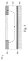
- FIG. 3 is a cross-sectional view of a passive device structure formed over a metal gate layer, in accordance with an embodiment of the invention.
- FIGS. 4( a ) and 4 ( b ) are cross-sectional views of a passive device structure formed over a metal gate layer, in accordance with another embodiment of the invention.
- the resulting resistor in passive device structures in effect becomes a parallel connection of the silicon resistance (R si ) and the metal gate resistance (R metal ), which lowers the resistance significantly.
- changing the doping concentration in the silicon layer does not modulate the overall resistance to a substantial degree, since metal is much more conductive and dominates the total resistance.
- the resistance of titanium nitride (TiN) is about 200 ⁇ /square, whereas passive devices require a target higher resistance (e.g., about 350 ⁇ /square) for 45 nm technology.
- an insulating layer such as aluminum oxide (Al 2 O 3 ) is formed between the metal gate layer and the silicon layer, thus effectively preventing current from flowing from the passive device layer (e.g., silicon) into the metal gate layer and undesirably decreasing the passive device resistance.
- the characteristics of the passive structure e.g., resistor, eFUSE, etc. may be determined by the silicon (semiconductor) layer, and not the combination of silicon and a metal layer therebeneath.
- the passive device structure 100 is a resistor formed in a semiconductor (e.g., polysilicon) layer 104 that may be doped in accordance with the desired characteristics (e.g., resistance value) of the device.
- Metal contact regions 106 e.g., silicide
- the resistor defines opposing terminals of the resistor.
- the resistance of the doped semiconductor layer 104 dominates the total resistance of the passive device 100 .
- the total effective resistance of the passive device 100 becomes a parallel connection of the semiconductor layer resistance (R si ) and the metal gate resistance (R metal ).
- FIG. 2( a ) is a cross-sectional view of another existing passive device structure 200 formed over a metal gate layer 202
- FIG. 2( b ) is a top view thereof
- the passive device structure 200 is an eFUSE formed in a semiconductor (e.g., polysilicon) layer 204 and having a top metal strip 206 (e.g., silicide) characterized by wide terminal portions 208 and a thin neck portion 210 connecting the terminal portions 208 .
- a semiconductor e.g., polysilicon
- a top metal strip 206 e.g., silicide
- an unprogrammed or low-resistance state of the structure 200 leaves the top metal strip portion of the device intact, and thus the presence of the metal gate layer 202 does not have as much of an impact on the desired device resistance as was the case for FIG. 1 .
- a void 212 or hole is intentionally created in the neck portion 210 of the strip 206 (such as by laser ablation or passing a high current therethrough) in order to set the eFUSE to a high-resistance state.
- the metal gate layer 202 once again provides a relatively low resistance parallel current path that can adversely affect desired device resistance characteristics.
- FIG. 3 there is shown a cross-sectional view of a passive device structure 300 formed over a metal gate layer 302 , in accordance with an embodiment of the invention.
- an electrically insulating layer 303 is formed over the metal gate layer 302 prior to deposition of the semiconductor layer 304 .
- the passive device e.g., a resistor
- the passive device is formed as known in the art such as by appropriate doping of the semiconductor layer 304 and silicide contact 306 formation to define opposing terminals of the passive device structure 300 .
- the metal gate layer 302 remains unpatterned therein.
- the insulator layer 303 may be an oxide layer or any suitable layer that acts as a barrier for electrical current from flowing through semiconductor layer 304 into the metal gate layer 302 and lowering the desired resistance of the device 300 .
- Exemplary suitable materials for the insulator layer 303 include, but are not limited to, aluminum oxide, zirconium oxide, hafnium oxide, hafnium silicate, silicon oxide, silicon nitride, lanthanum oxide, and combinations thereof
- the insulator layer 303 may be formed by any suitable techniques such as physical vapor deposition (PLD), atomic layer deposition (ALD) and the like.
- An exemplary thickness for the insulator layer 303 may be on the order of about 10 to about 200 nanometers (nm), and more specifically about 10 to about 100 nm.
- a 12-angstrom ( ⁇ ) layer of aluminum oxide (Al 2 O 3 ) is shown to effectively block an amorphous silicon/metal gate layer conductive path and provide a resistance of about 6 ⁇ 10 4 ⁇ /square in the absence of doping in the silicon layer. Accordingly, specific resistance targets for passive devices may now be easily achieved through appropriate semiconductor layer doping, without adverse effects due to the now more common metal gate technology in CMOS devices.
- FIGS. 4( a ) and 4 ( b ) are cross-sectional views of a passive device structure 400 formed over a metal gate layer 402 , in accordance with an embodiment of the invention.
- the insulator layer 403 is formed over the metal gate layer 402 prior to deposition of the semiconductor layer 404 and formation of the passive device structure 406 , which in this example is an eFUSE.
- the device 400 is in an unprogrammed state
- FIG. 4( b ) the device 400 is in a programmed or “blown” state. In either instance, it will be seen that no substantial leakage current path from the semiconductor layer 404 is allowed to pass through the metal gate layer 402 .
Landscapes
- Design And Manufacture Of Integrated Circuits (AREA)
Abstract
Description
Claims (14)
Priority Applications (1)
| Application Number | Priority Date | Filing Date | Title |
|---|---|---|---|
| US12/543,544 US8097520B2 (en) | 2009-08-19 | 2009-08-19 | Integration of passive device structures with metal gate layers |
Applications Claiming Priority (1)
| Application Number | Priority Date | Filing Date | Title |
|---|---|---|---|
| US12/543,544 US8097520B2 (en) | 2009-08-19 | 2009-08-19 | Integration of passive device structures with metal gate layers |
Publications (2)
| Publication Number | Publication Date |
|---|---|
| US20110042786A1 US20110042786A1 (en) | 2011-02-24 |
| US8097520B2 true US8097520B2 (en) | 2012-01-17 |
Family
ID=43604649
Family Applications (1)
| Application Number | Title | Priority Date | Filing Date |
|---|---|---|---|
| US12/543,544 Expired - Fee Related US8097520B2 (en) | 2009-08-19 | 2009-08-19 | Integration of passive device structures with metal gate layers |
Country Status (1)
| Country | Link |
|---|---|
| US (1) | US8097520B2 (en) |
Cited By (1)
| Publication number | Priority date | Publication date | Assignee | Title |
|---|---|---|---|---|
| US20120098071A1 (en) * | 2010-10-25 | 2012-04-26 | Texas Instruments Incorporated | High Sheet Resistor in CMOS Flow |
Families Citing this family (1)
| Publication number | Priority date | Publication date | Assignee | Title |
|---|---|---|---|---|
| EP4018013A4 (en) * | 2019-09-13 | 2022-12-14 | Versum Materials US, LLC | MONOALCOXYSILANEES AND DENSE ORGANOSILICON FILMS MADE FROM THEM |
Citations (43)
| Publication number | Priority date | Publication date | Assignee | Title |
|---|---|---|---|---|
| US4404581A (en) | 1980-12-15 | 1983-09-13 | Rockwell International Corporation | ROM With redundant ROM cells employing a highly resistive polysilicon film for programming the cells |
| US4604641A (en) | 1981-11-30 | 1986-08-05 | Tokyo Shibaura Denki Kabushiki Kaisha | Semiconductor device and method for manufacturing the same |
| US4878770A (en) | 1987-09-09 | 1989-11-07 | Analog Devices, Inc. | IC chips with self-aligned thin film resistors |
| US5116770A (en) | 1988-07-14 | 1992-05-26 | Matsushita Electric Industrial Co., Ltd. | Method for fabricating bipolar semiconductor devices |
| US5189284A (en) | 1988-02-29 | 1993-02-23 | Fuji Xerox Co., Ltd. | Resistor, process for producing the same, and thermal head using the same |
| US5236851A (en) | 1988-07-14 | 1993-08-17 | Matsushita Electric Industrial Co., Ltd. | Method for fabricating semiconductor devices |
| US5465005A (en) | 1991-10-30 | 1995-11-07 | Texas Instruments Incorporated | Polysilicon resistor structure including polysilicon contacts |
| US5530418A (en) | 1995-07-26 | 1996-06-25 | Taiwan Semiconductor Manufacturing Company | Method for shielding polysilicon resistors from hydrogen intrusion |
| US5585663A (en) | 1994-06-10 | 1996-12-17 | International Business Machines Corporation | Self cooling electrically programmable fuse |
| US5838044A (en) | 1995-12-12 | 1998-11-17 | Advanced Micro Devices | Integrated circuit having improved polysilicon resistor structures |
| US6013940A (en) | 1994-08-19 | 2000-01-11 | Seiko Instruments Inc. | Poly-crystalline silicon film ladder resistor |
| US6100746A (en) | 1998-05-18 | 2000-08-08 | Vanguard International Semiconductor Corporation | Electrically programmable fuse |
| US6112765A (en) | 1998-05-26 | 2000-09-05 | Caterpillar Inc. | Method and apparatus for monitoring operation of a gaseous fuel admission valve |
| US6184103B1 (en) * | 1998-06-26 | 2001-02-06 | Sony Corporation | High resistance polysilicon SRAM load elements and methods of fabricating therefor |
| US6265746B1 (en) | 1998-05-28 | 2001-07-24 | Altera Corporation | Highly resistive interconnects |
| US6326256B1 (en) | 1998-12-18 | 2001-12-04 | Texas Instruments Incorporated | Method of producing a laser trimmable thin film resistor in an integrated circuit |
| US6522200B2 (en) | 2000-12-11 | 2003-02-18 | Texas Instruments Incorporated | Process-insensitive, highly-linear constant transconductance circuit |
| US6542419B2 (en) | 2000-08-24 | 2003-04-01 | Kabushiki Kaisha Toshiba | Semiconductor integrated circuit device with electrically programmable fuse |
| US20040183157A1 (en) * | 2003-01-29 | 2004-09-23 | Hitachi, Ltd. | Semiconductor device and manufacturing method of the same |
| US6876594B2 (en) | 2002-12-26 | 2005-04-05 | Texas Instruments Incorporated | Integrated circuit with programmable fuse array |
| US7008833B2 (en) | 2004-01-12 | 2006-03-07 | Sharp Laboratories Of America, Inc. | In2O3thin film resistivity control by doping metal oxide insulator for MFMox device applications |
| US20060102963A1 (en) | 2004-11-15 | 2006-05-18 | Taiwan Semiconductor Manufacturing Co., Ltd. | Passive device and method for forming the same |
| US7049929B1 (en) | 2001-05-01 | 2006-05-23 | Tessera, Inc. | Resistor process |
| US20060118885A1 (en) * | 2004-12-06 | 2006-06-08 | Samsung Electronics Co., Ltd. | Semiconductor device having resistor and method of fabricating the same |
| US7060612B2 (en) | 2004-08-26 | 2006-06-13 | International Business Machines Corporation | Method of adjusting resistors post silicide process |
| US7112535B2 (en) | 2003-09-30 | 2006-09-26 | International Business Machines Corporation | Precision polysilicon resistor process |
| US7200064B1 (en) | 2005-10-07 | 2007-04-03 | International Business Machines Corporation | Apparatus and method for providing a reprogrammable electrically programmable fuse |
| US7215177B2 (en) | 2005-01-12 | 2007-05-08 | Kabushiki Kaisha Toshiba | Semiconductor integrated circuit with electrically programmable fuse |
| US7242072B2 (en) | 2004-11-23 | 2007-07-10 | International Business Machines Corporation | Electrically programmable fuse for silicon-on-insulator (SOI) technology |
| US7268577B2 (en) | 2004-12-17 | 2007-09-11 | International Business Machines Corporation | Changing chip function based on fuse states |
| US7285472B2 (en) | 2005-01-27 | 2007-10-23 | International Business Machines Corporation | Low tolerance polysilicon resistor for low temperature silicide processing |
| US7288804B2 (en) | 2006-03-09 | 2007-10-30 | International Business Machines Corporation | Electrically programmable π-shaped fuse structures and methods of fabrication thereof |
| US7307911B1 (en) | 2006-07-27 | 2007-12-11 | International Business Machines Corporation | Apparatus and method for improving sensing margin of electrically programmable fuses |
| US7315193B2 (en) | 2005-08-24 | 2008-01-01 | International Business Machines Corporation | Circuitry and method for programming an electrically programmable fuse |
| US7323761B2 (en) | 2004-11-12 | 2008-01-29 | International Business Machines Corporation | Antifuse structure having an integrated heating element |
| US7334320B2 (en) | 2003-12-03 | 2008-02-26 | International Business Machines Corporation | Method of making an electronic fuse with improved ESD tolerance |
| US7339400B1 (en) | 2006-06-09 | 2008-03-04 | Xilinx, Inc. | Interface port for electrically programmed fuses in a programmable logic device |
| US7345943B2 (en) | 2006-06-28 | 2008-03-18 | International Business Machines Corporation | Unclocked eFUSE circuit |
| US7345904B1 (en) | 2006-10-11 | 2008-03-18 | International Business Machines Corporation | Method for programming an electronically programmable semiconductor fuse |
| US7382036B2 (en) | 2005-07-29 | 2008-06-03 | International Business Machines Corporation | Doped single crystal silicon silicided eFuse |
| US20090090977A1 (en) * | 2007-10-09 | 2009-04-09 | International Business Machines Corporation | Resistor and fet formed from the metal portion of a mosfet metal gate stack |
| US20100006841A1 (en) * | 2008-07-11 | 2010-01-14 | International Business Machines Corporation | Dual metal gate transistor with resistor having dielectric layer between metal and polysilicon |
| US20110037128A1 (en) * | 2009-08-15 | 2011-02-17 | International Business Machines Corporation | Method and structure for improving uniformity of passive devices in metal gate technology |
-
2009
- 2009-08-19 US US12/543,544 patent/US8097520B2/en not_active Expired - Fee Related
Patent Citations (49)
| Publication number | Priority date | Publication date | Assignee | Title |
|---|---|---|---|---|
| US4404581A (en) | 1980-12-15 | 1983-09-13 | Rockwell International Corporation | ROM With redundant ROM cells employing a highly resistive polysilicon film for programming the cells |
| US4604641A (en) | 1981-11-30 | 1986-08-05 | Tokyo Shibaura Denki Kabushiki Kaisha | Semiconductor device and method for manufacturing the same |
| US4878770A (en) | 1987-09-09 | 1989-11-07 | Analog Devices, Inc. | IC chips with self-aligned thin film resistors |
| US5043295A (en) | 1987-09-09 | 1991-08-27 | Ruggerio Paul A | Method of forming an IC chip with self-aligned thin film resistors |
| US5189284A (en) | 1988-02-29 | 1993-02-23 | Fuji Xerox Co., Ltd. | Resistor, process for producing the same, and thermal head using the same |
| US5116770A (en) | 1988-07-14 | 1992-05-26 | Matsushita Electric Industrial Co., Ltd. | Method for fabricating bipolar semiconductor devices |
| US5236851A (en) | 1988-07-14 | 1993-08-17 | Matsushita Electric Industrial Co., Ltd. | Method for fabricating semiconductor devices |
| US5465005A (en) | 1991-10-30 | 1995-11-07 | Texas Instruments Incorporated | Polysilicon resistor structure including polysilicon contacts |
| US6261915B1 (en) | 1991-10-30 | 2001-07-17 | Texas Instruments Incorporated | Process of making polysilicon resistor |
| US5585663A (en) | 1994-06-10 | 1996-12-17 | International Business Machines Corporation | Self cooling electrically programmable fuse |
| US5622892A (en) | 1994-06-10 | 1997-04-22 | International Business Machines Corporation | Method of making a self cooling electrically programmable fuse |
| US6013940A (en) | 1994-08-19 | 2000-01-11 | Seiko Instruments Inc. | Poly-crystalline silicon film ladder resistor |
| US5530418A (en) | 1995-07-26 | 1996-06-25 | Taiwan Semiconductor Manufacturing Company | Method for shielding polysilicon resistors from hydrogen intrusion |
| US5838044A (en) | 1995-12-12 | 1998-11-17 | Advanced Micro Devices | Integrated circuit having improved polysilicon resistor structures |
| US6100746A (en) | 1998-05-18 | 2000-08-08 | Vanguard International Semiconductor Corporation | Electrically programmable fuse |
| US6285238B1 (en) | 1998-05-18 | 2001-09-04 | Vanguard International Semiconductor Corporation | Electrically programmable fuse |
| US6392468B1 (en) | 1998-05-18 | 2002-05-21 | Vanguard International Semiconductor Corporation | Electrically programmable fuse |
| US6112765A (en) | 1998-05-26 | 2000-09-05 | Caterpillar Inc. | Method and apparatus for monitoring operation of a gaseous fuel admission valve |
| US6265746B1 (en) | 1998-05-28 | 2001-07-24 | Altera Corporation | Highly resistive interconnects |
| US6184103B1 (en) * | 1998-06-26 | 2001-02-06 | Sony Corporation | High resistance polysilicon SRAM load elements and methods of fabricating therefor |
| US6326256B1 (en) | 1998-12-18 | 2001-12-04 | Texas Instruments Incorporated | Method of producing a laser trimmable thin film resistor in an integrated circuit |
| US6542419B2 (en) | 2000-08-24 | 2003-04-01 | Kabushiki Kaisha Toshiba | Semiconductor integrated circuit device with electrically programmable fuse |
| US6522200B2 (en) | 2000-12-11 | 2003-02-18 | Texas Instruments Incorporated | Process-insensitive, highly-linear constant transconductance circuit |
| US7049929B1 (en) | 2001-05-01 | 2006-05-23 | Tessera, Inc. | Resistor process |
| US6876594B2 (en) | 2002-12-26 | 2005-04-05 | Texas Instruments Incorporated | Integrated circuit with programmable fuse array |
| US20040183157A1 (en) * | 2003-01-29 | 2004-09-23 | Hitachi, Ltd. | Semiconductor device and manufacturing method of the same |
| US7112535B2 (en) | 2003-09-30 | 2006-09-26 | International Business Machines Corporation | Precision polysilicon resistor process |
| US7334320B2 (en) | 2003-12-03 | 2008-02-26 | International Business Machines Corporation | Method of making an electronic fuse with improved ESD tolerance |
| US7008833B2 (en) | 2004-01-12 | 2006-03-07 | Sharp Laboratories Of America, Inc. | In2O3thin film resistivity control by doping metal oxide insulator for MFMox device applications |
| US7060612B2 (en) | 2004-08-26 | 2006-06-13 | International Business Machines Corporation | Method of adjusting resistors post silicide process |
| US7323761B2 (en) | 2004-11-12 | 2008-01-29 | International Business Machines Corporation | Antifuse structure having an integrated heating element |
| US20060102963A1 (en) | 2004-11-15 | 2006-05-18 | Taiwan Semiconductor Manufacturing Co., Ltd. | Passive device and method for forming the same |
| US7242072B2 (en) | 2004-11-23 | 2007-07-10 | International Business Machines Corporation | Electrically programmable fuse for silicon-on-insulator (SOI) technology |
| US20060118885A1 (en) * | 2004-12-06 | 2006-06-08 | Samsung Electronics Co., Ltd. | Semiconductor device having resistor and method of fabricating the same |
| US7268577B2 (en) | 2004-12-17 | 2007-09-11 | International Business Machines Corporation | Changing chip function based on fuse states |
| US7336095B2 (en) | 2004-12-17 | 2008-02-26 | International Business Machines Corporation | Changing chip function based on fuse states |
| US7215177B2 (en) | 2005-01-12 | 2007-05-08 | Kabushiki Kaisha Toshiba | Semiconductor integrated circuit with electrically programmable fuse |
| US7285472B2 (en) | 2005-01-27 | 2007-10-23 | International Business Machines Corporation | Low tolerance polysilicon resistor for low temperature silicide processing |
| US7382036B2 (en) | 2005-07-29 | 2008-06-03 | International Business Machines Corporation | Doped single crystal silicon silicided eFuse |
| US7315193B2 (en) | 2005-08-24 | 2008-01-01 | International Business Machines Corporation | Circuitry and method for programming an electrically programmable fuse |
| US7200064B1 (en) | 2005-10-07 | 2007-04-03 | International Business Machines Corporation | Apparatus and method for providing a reprogrammable electrically programmable fuse |
| US7288804B2 (en) | 2006-03-09 | 2007-10-30 | International Business Machines Corporation | Electrically programmable π-shaped fuse structures and methods of fabrication thereof |
| US7339400B1 (en) | 2006-06-09 | 2008-03-04 | Xilinx, Inc. | Interface port for electrically programmed fuses in a programmable logic device |
| US7345943B2 (en) | 2006-06-28 | 2008-03-18 | International Business Machines Corporation | Unclocked eFUSE circuit |
| US7307911B1 (en) | 2006-07-27 | 2007-12-11 | International Business Machines Corporation | Apparatus and method for improving sensing margin of electrically programmable fuses |
| US7345904B1 (en) | 2006-10-11 | 2008-03-18 | International Business Machines Corporation | Method for programming an electronically programmable semiconductor fuse |
| US20090090977A1 (en) * | 2007-10-09 | 2009-04-09 | International Business Machines Corporation | Resistor and fet formed from the metal portion of a mosfet metal gate stack |
| US20100006841A1 (en) * | 2008-07-11 | 2010-01-14 | International Business Machines Corporation | Dual metal gate transistor with resistor having dielectric layer between metal and polysilicon |
| US20110037128A1 (en) * | 2009-08-15 | 2011-02-17 | International Business Machines Corporation | Method and structure for improving uniformity of passive devices in metal gate technology |
Cited By (5)
| Publication number | Priority date | Publication date | Assignee | Title |
|---|---|---|---|---|
| US20120098071A1 (en) * | 2010-10-25 | 2012-04-26 | Texas Instruments Incorporated | High Sheet Resistor in CMOS Flow |
| US8580631B2 (en) * | 2010-10-25 | 2013-11-12 | Texas Instruments Incorporated | High sheet resistor in CMOS flow |
| US9006838B2 (en) | 2010-10-25 | 2015-04-14 | Texas Instruments Incorporated | High sheet resistor in CMOS flow |
| US9362270B2 (en) | 2010-10-25 | 2016-06-07 | Texas Instruments Incorporated | High sheet resistor in CMOS flow |
| US9698211B2 (en) | 2010-10-25 | 2017-07-04 | Texas Instruments Incorporated | High sheet resistor in CMOS flow |
Also Published As
| Publication number | Publication date |
|---|---|
| US20110042786A1 (en) | 2011-02-24 |
Similar Documents
| Publication | Publication Date | Title |
|---|---|---|
| US8159040B2 (en) | Metal gate integration structure and method including metal fuse, anti-fuse and/or resistor | |
| US7825479B2 (en) | Electrical antifuse having a multi-thickness dielectric layer | |
| JP3256603B2 (en) | Semiconductor device and manufacturing method thereof | |
| US9437593B2 (en) | Silicided semiconductor structure and method of forming the same | |
| US8163640B2 (en) | Metal gate compatible electrical fuse | |
| US11257750B2 (en) | E-fuse co-processed with MIM capacitor | |
| JPH04229635A (en) | Integrated circuit provided with antifuse | |
| US20080029843A1 (en) | E-Fuse and Method for Fabricating E-Fuses Integrating Polysilicon Resistor Masks | |
| JP4651848B2 (en) | Semiconductor device, manufacturing method thereof, and CMOS transistor | |
| US20130320488A1 (en) | System and method for forming aluminum fuse for compatibility with copper beol interconnect scheme | |
| US8754498B2 (en) | Antifuse and method of making the antifuse | |
| US20070284693A1 (en) | Electrically programmable fuse with asymmetric structure | |
| US8004060B2 (en) | Metal gate compatible electrical antifuse | |
| US6885280B2 (en) | High value split poly p-resistor with low standard deviation | |
| US20110156146A1 (en) | eFUSE ENABLEMENT WITH THIN POLYSILICON OR AMORPHOUS-SILICON GATE-STACK FOR HKMG CMOS | |
| US8097520B2 (en) | Integration of passive device structures with metal gate layers | |
| US20090135640A1 (en) | Electromigration-programmable semiconductor device with bidirectional resistance change | |
| US8481397B2 (en) | Polysilicon resistor and E-fuse for integration with metal gate and high-k dielectric | |
| US8241986B2 (en) | Semiconductor device and process for reducing damaging breakdown in gate dielectrics | |
| CN107622991A (en) | Electric fuse structure and manufacturing method thereof | |
| CN116093067B (en) | Fuse structure, forming method and programmable memory | |
| US20230135418A1 (en) | Fuse structure, method for manufacturing same and programmable memory | |
| CN117377314A (en) | Semiconductor components | |
| US20250031586A1 (en) | Carbon film integrated into a back end of line process | |
| TWI856303B (en) | Methods of forming semiconductor devices |
Legal Events
| Date | Code | Title | Description |
|---|---|---|---|
| AS | Assignment |
Owner name: INTERNATIONAL BUSINESS MACHINES CORPORATION, NEW Y Free format text: ASSIGNMENT OF ASSIGNORS INTEREST;ASSIGNORS:BU, HUIMING;CHAKRAVARTI, SATYA N.;GUO, DECHAO;AND OTHERS;SIGNING DATES FROM 20090817 TO 20090818;REEL/FRAME:023115/0122 |
|
| STCF | Information on status: patent grant |
Free format text: PATENTED CASE |
|
| FPAY | Fee payment |
Year of fee payment: 4 |
|
| AS | Assignment |
Owner name: GLOBALFOUNDRIES U.S. 2 LLC, NEW YORK Free format text: ASSIGNMENT OF ASSIGNORS INTEREST;ASSIGNOR:INTERNATIONAL BUSINESS MACHINES CORPORATION;REEL/FRAME:036550/0001 Effective date: 20150629 |
|
| AS | Assignment |
Owner name: GLOBALFOUNDRIES INC., CAYMAN ISLANDS Free format text: ASSIGNMENT OF ASSIGNORS INTEREST;ASSIGNORS:GLOBALFOUNDRIES U.S. 2 LLC;GLOBALFOUNDRIES U.S. INC.;REEL/FRAME:036779/0001 Effective date: 20150910 |
|
| AS | Assignment |
Owner name: WILMINGTON TRUST, NATIONAL ASSOCIATION, DELAWARE Free format text: SECURITY AGREEMENT;ASSIGNOR:GLOBALFOUNDRIES INC.;REEL/FRAME:049490/0001 Effective date: 20181127 |
|
| FEPP | Fee payment procedure |
Free format text: MAINTENANCE FEE REMINDER MAILED (ORIGINAL EVENT CODE: REM.); ENTITY STATUS OF PATENT OWNER: LARGE ENTITY |
|
| LAPS | Lapse for failure to pay maintenance fees |
Free format text: PATENT EXPIRED FOR FAILURE TO PAY MAINTENANCE FEES (ORIGINAL EVENT CODE: EXP.); ENTITY STATUS OF PATENT OWNER: LARGE ENTITY |
|
| STCH | Information on status: patent discontinuation |
Free format text: PATENT EXPIRED DUE TO NONPAYMENT OF MAINTENANCE FEES UNDER 37 CFR 1.362 |
|
| FP | Lapsed due to failure to pay maintenance fee |
Effective date: 20200117 |
|
| AS | Assignment |
Owner name: GLOBALFOUNDRIES INC., CAYMAN ISLANDS Free format text: RELEASE BY SECURED PARTY;ASSIGNOR:WILMINGTON TRUST, NATIONAL ASSOCIATION;REEL/FRAME:054636/0001 Effective date: 20201117 |
|
| AS | Assignment |
Owner name: GLOBALFOUNDRIES U.S. INC., NEW YORK Free format text: RELEASE BY SECURED PARTY;ASSIGNOR:WILMINGTON TRUST, NATIONAL ASSOCIATION;REEL/FRAME:056987/0001 Effective date: 20201117 Owner name: GLOBALFOUNDRIES U.S. INC., NEW YORK Free format text: RELEASE OF SECURITY INTEREST;ASSIGNOR:WILMINGTON TRUST, NATIONAL ASSOCIATION;REEL/FRAME:056987/0001 Effective date: 20201117 |