US8094367B2 - Optically locked photon echo apparatus and method - Google Patents
Optically locked photon echo apparatus and method Download PDFInfo
- Publication number
- US8094367B2 US8094367B2 US12/857,537 US85753710A US8094367B2 US 8094367 B2 US8094367 B2 US 8094367B2 US 85753710 A US85753710 A US 85753710A US 8094367 B2 US8094367 B2 US 8094367B2
- Authority
- US
- United States
- Prior art keywords
- optical
- light
- photon echo
- pulses
- optically locked
- Prior art date
- Legal status (The legal status is an assumption and is not a legal conclusion. Google has not performed a legal analysis and makes no representation as to the accuracy of the status listed.)
- Expired - Fee Related
Links
Images


Classifications
-
- G—PHYSICS
- G02—OPTICS
- G02F—OPTICAL DEVICES OR ARRANGEMENTS FOR THE CONTROL OF LIGHT BY MODIFICATION OF THE OPTICAL PROPERTIES OF THE MEDIA OF THE ELEMENTS INVOLVED THEREIN; NON-LINEAR OPTICS; FREQUENCY-CHANGING OF LIGHT; OPTICAL LOGIC ELEMENTS; OPTICAL ANALOGUE/DIGITAL CONVERTERS
- G02F1/00—Devices or arrangements for the control of the intensity, colour, phase, polarisation or direction of light arriving from an independent light source, e.g. switching, gating or modulating; Non-linear optics
- G02F1/35—Non-linear optics
- G02F1/3515—All-optical modulation, gating, switching, e.g. control of a light beam by another light beam
-
- G—PHYSICS
- G02—OPTICS
- G02F—OPTICAL DEVICES OR ARRANGEMENTS FOR THE CONTROL OF LIGHT BY MODIFICATION OF THE OPTICAL PROPERTIES OF THE MEDIA OF THE ELEMENTS INVOLVED THEREIN; NON-LINEAR OPTICS; FREQUENCY-CHANGING OF LIGHT; OPTICAL LOGIC ELEMENTS; OPTICAL ANALOGUE/DIGITAL CONVERTERS
- G02F2203/00—Function characteristic
- G02F2203/26—Pulse shaping; Apparatus or methods therefor
Definitions
- quantum optical data is necessary for quantum information processing ranging from quantum computers that require a shorter storage time to quantum communications such as long distance quantum cryptography that requires a longer storage time.
- the storage time of three-pulse photon echoes is limited by the optical population decay time and is similar to the optical phase relaxation time. Unlike the two-pulse photon echoes, three pulse photon echoes cannot retrieve more than 50% of stored information due to optical coherence loss attributable to optical population decay.
- phase-locked echo methods the storage time is extended from optical phase relaxation time to spin dephasing time, which is inversely proportional to spin inhomogeneous broadening [B. S. Ham, Opt. Exp. Vol. 18, No. 2, pp. 1704-1713 (2010)].
- phase inversion is realized using an externally applied Direct Current (DC) voltage or a magnetic field gradient, where spontaneous emission noise caused by a rephasing pulse in conventional two-pulse photon echoes is eliminated.
- DC Direct Current
- the storage time in CRIB is still limited by the optical phase relaxation time, which is much shorter than a millisecond [M. Nilsson and S. Kroll, Opt. Commun. Vol. 247 (No. 4-6), pp. 393-403 (2005)].
- an object of the present invention is to provide an optically locked photon echo apparatus and method, which can solve the problem of limited echo efficiency and can overcome constraints on the conventional storage time being limited to the spin dephasing time.
- Another object of the present invention is to provide an optically locked photon echo apparatus and method, which extend the storage time up to spin population relaxation time while obtaining more than 50% retrieval efficiency because the present invention locks even the phase evolution of individual atoms as well as an optical population decay process, unlike the conventional version of phase-locked photon echoes.
- a further explanation thereof may be given in such a way that, in rare-earth-doped crystal such as Pr 3+ -doped Y 2 SiO 5 , the spin population relaxation time is at least a million times as long as the spin dephasing time which is the limit of the storage time of conventional three-pulse photon echoes.
- a further object of the present invention is to provide an optically locked photon echo apparatus and method, which causes the storage time to be unchanged even by spin dephasing caused by spin inhomogeneous broadening. Thanking to the inherent optical phase locking characteristics of three-pulse photon echoes, preventing optical coherence loss from population decay the optically locked echo provides ultralong photon storage time with more than 50% retrieval efficiency.
- the five or more optical pulses fall into a first optical pulse group including one or more of optical pulses corresponding to input light (D), write light (W) and read light (R) which resonate between the energy levels
- the three energy levels are set in such a way that the energy levels
- a time interval between the input light (D) and the write light (W) is shorter than an optical phase relaxation time, but has a length sufficient to fall within the spectral width of the system.
- a time interval between the first control light (B 1 ) and the second control light (B 2 ) is shorter than a spin population relaxation time.
- areas of the pulses corresponding to the first control light (B 1 ) and the second control light (B 2 ) are ⁇ and 3 ⁇ , respectively, and a sum of the areas of these pulses is 4 ⁇ .
- the nonlinear optical medium is a solid, multiply coupled semiconductors, or a cold atom ensemble.
- the present invention provides an optically locked photon echo method for generating output light (E), which satisfies a phase matching condition, using an optically locked photon echo apparatus, the apparatus including a nonlinear optical medium provided with three energy levels
- FIGS. 1A and 1B are respectively a configuration diagram of an optically locked photon echo apparatus and a diagram of the energy levels of an optical medium interacting with optical pulses according to an embodiment of the present invention
- FIG. 2 is a diagram showing the optically locked photon echo apparatus according to an embodiment of the present invention.
- FIG. 3 is a diagram showing the sequence of optical pulses for optically locked photon echoes according to the present invention
- FIG. 4 is a flowchart showing an optically locked photon echo method according to the present invention.
- FIGS. 5A to 5D are diagrams showing the results of numerical simulations of typical two-pulse photon echoes
- FIGS. 6A to 6D are diagrams showing the results of numerical simulations of three-pulse photon echoes
- FIGS. 7A to 7F are diagrams showing the comparison between the results of numerical simulations of the three-pulse photon echoes and optically locked photon echoes;
- FIGS. 8A to 8D are diagrams showing the results of detailed numerical simulations for describing the optical locking of FIG. 7B ;
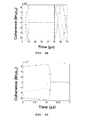
- FIGS. 9A and 9B are diagrams showing the experimental results of the optically locked photon echoes according to the present invention.
- FIGS. 1A and 1B are respectively a configuration diagram of an optically locked photon echo apparatus and a diagram of the energy levels of an optical medium interacting with optical pulses according to an embodiment of the present invention.
- the optically locked photon echo apparatus includes an optical medium 10 , and an optical pulse generation unit 20 for generating five or more optical pulses resonating between the energy levels of the optical medium 10 .
- the optical medium 10 has nonlinear optical characteristics and has three energy levels
- the optical medium 10 can be a solid such as a rare-earth Pr 3+ doped Y 2 SiO 5 , multiply coupled semiconductors, or a cold atomic ensemble.
- FIG. 1B illustrates the energy levels of the optical medium 10 which interacts with the five or more optical pulses.
- 2 > are in a ground state, and the energy level
- FIGS. 1A and 1B will be described in detail below.
- the five or more optical pulses fall into a first optical pulse group f 1 including optical pulses corresponding to one or more input lights D, write light W and read light R which resonate between the energy levels
- the five or more optical pulses are incident on the optical medium 10 after having passed through an optical fiber, surface plasmon medium or free space.
- the first optical pulse group f 1 and the second optical pulse group f 2 are implemented using light having different wavelengths or polarization.
- the first optical pulse group f 1 is used for the input light D, the write light W, and the read light R.
- the second optical pulse group f 2 has the first control light B 1 used to transfer excited atoms in state
- the input light D may include one or more lights, and the time interval between the first control light B 1 and the second control light B 2 must be shorter than the spin population relaxation time.
- the time interval between the input light D and the write light W must be shorter than the optical phase relaxation time, but has a length sufficient to fall within the spectral width of the system.
- the output light E satisfies a phase matching condition for the five or more optical pulses.
- FIG. 2 illustrates an optically locked photon echo apparatus according to an embodiment of the present invention.
- the optical pulse generation unit 20 of the optically locked photon echo apparatus includes a first light source 21 for outputting laser light; a second light source 22 for outputting laser light; a first optical modulation module 23 for modulating the laser light from the first light source 21 into an optical pulse train so as to generate some of the five or more optical pulses, a second optical modulation module 24 for modulating the laser light from the second light source 22 into an optical pulse train so as to generate the remaining optical pulses, which are different from the optical pulses generated by the first optical modulation module 23 among the five or more optical pulses; and a control module 25 for generating a synchronous signal required to synchronize the optical pulse trains output from the first and second optical modulation modules 23 and 24 with each other.
- FIG. 3 illustrates the sequence of optical pulses for optically locked photon echoes according to the present invention.
- the optical pulses are incident on the optical medium 10 in the sequence of the input light D, the write light W, the first control light B 1 , the second control light B 2 and the read light R, and the output light E is generated last of all as a result.
- T i is the time at which an optical pulse i arrives at the optical medium.
- FIG. 4 is a flowchart showing an optically locked photon echo method according to the present invention to describe FIG. 3 in detail.
- the optically locked photon echo method can be implemented according to the following sequence.
- the optically locked photon echo method includes the step S 110 of input light D being incident on the optical medium 10 ; the step S 115 of the write light W being incident on the optical medium 10 ; the step S 120 of the input light D and the write light W, which are temporally separated from each other, forming a spectral grating in cooperation with each other; the step S 125 of the first control light B 1 being incident on the optical medium 10 ; the step S 130 of the second control light B 2 being incident on the optical medium 10 ; the step S 135 of the read light R being incident on the optical medium 10 ; the step S 140 of reproducing the information of the input light D, stored in the spectral grating, using the read light R; and the step S 145 of the input light D, the write light W and the read light R generating the output light E which satisfies the phase matching condition via interaction with the optical medium 10 .
- the term “spectral grating” means that the information of the input light D is stored. However, it means that the information is stored in the wide frequency band of relevant atoms.
- the output light E is determined by performing four-wave mixing generation.
- FIGS. 5A to 5D illustrate the results of numerical simulations of conventional two-pulse photon echoes.
- FIG. 5A illustrates the sequence of pulses corresponding to the input light D and the write light W resonating between the energy levels
- the write light W needs perfect rephasing, so that the pulse width of W must be t.
- FIG. 5C illustrates the sum of phase coherences exhibited by the individual atoms of FIG. 5B .
- FIG. 5D illustrates the phase evolution of atoms detuned to resonant laser light over time. This detuning occurs because the optical medium is inhomogeneous, wherein detuned values are determined on the basis of inhomogeneous broadening of the atoms. In this case, conditions for the inhomogeneous broadening of atoms are the fundamental basis of photon echoes based on a rephasing process.
- FIGS. 6A to 6D are diagrams showing the results of numerical simulations of conventional three-pulse photon echoes.
- the write light W of FIGS. 5A to 5D is divided into two ⁇ /2 pulses, as shown in FIG. 6 .
- This division is required in the three-pulse photon echoes to form a spectral grating according to the population inversion between the ground state and the excited state, rather than to perform rephasing which is the core principle of the two-pulse photon echoes.
- the information of the input light D is stored in the spectral grating.
- the final results are identical to those of FIGS. 5A to 5D except for the delay time.
- the three-pulse photon echoes are intended to extend the storage time, which is due to the fact that the optical population decay time is longer than the phase relaxation time.
- the initial coherence additionally decreases.
- coherence loss is more than 50%, and thus the three-pulse photon echoes cannot be applied to quantum memory.
- FIG. 7E shows the reason why the magnitude of the echo of FIG. 7A is less than that of FIG. 7B , which is that in the case of the phase evolution of the individual atoms, the phase coherence is rapidly weakened and the relative coherence is also rapidly lost due to optical population loss.
- FIG. 8A illustrates the results of numerical simulations of the phase evolution of symmetrical atoms which are identical to those of FIG. 7F .
- two-photon coherence Re( ⁇ 12 ) is created using the transfer of the population from the excited state
- the two-photon coherence in such population transfer induction is more temporally stable than that of conventional phase-locked two-photon coherence.
- optical coherence created by the input light D and the write light W is replaced with spin coherence by the first control light B 1 , and is then stored. Since the spin population relaxation time is much longer than the optical population decay time, it can be stored for a longer time. In contrast, the storage time is limited by the optical population decay time in the conventional three-pulse photon echo scheme.
- FIGS. 9A and 9B are diagrams illustrating the experimental results of the optically locked photon echoes according to the present invention.
- the present invention can provide an optically locked photon echo apparatus and method, which can solve the problem of limited echo efficiency and can overcome constraints on the conventional storage time being limited to the spin dephasing time.
- the present invention is advantageous in that it can halt the phase evolution of individual atoms as well as optical population decay, unlike the phase-locked photon echoes, thus extending the storage time up to the spin population relaxation time while obtaining more than 50% retrieval efficiency.
- the present invention is advantageous in that the storage time can be unchanged even by spin dephasing caused by spin inhomogeneous broadening, thanks to the inherent optical phase locking characteristics of three-pulse photon echoes, unlike phase-locked photon echoes while preventing optical coherence loss from occurring during the storage time.
Landscapes
- Physics & Mathematics (AREA)
- Nonlinear Science (AREA)
- General Physics & Mathematics (AREA)
- Optics & Photonics (AREA)
- Optical Modulation, Optical Deflection, Nonlinear Optics, Optical Demodulation, Optical Logic Elements (AREA)
Abstract
Description
k E +k D =k W +k R (1)
f E =f D =f W +f R (2)
where ki is the propagation vector of an optical pulse i and fi is the frequency of the optical pulse i.
Claims (18)
Applications Claiming Priority (2)
| Application Number | Priority Date | Filing Date | Title |
|---|---|---|---|
| KR1020100022444A KR101063508B1 (en) | 2010-03-12 | 2010-03-12 | Photo-Lock Photon Eco Apparatus and Method |
| KR10-2010-0022444 | 2010-03-12 |
Publications (2)
| Publication Number | Publication Date |
|---|---|
| US20110222387A1 US20110222387A1 (en) | 2011-09-15 |
| US8094367B2 true US8094367B2 (en) | 2012-01-10 |
Family
ID=44559869
Family Applications (1)
| Application Number | Title | Priority Date | Filing Date |
|---|---|---|---|
| US12/857,537 Expired - Fee Related US8094367B2 (en) | 2010-03-12 | 2010-08-16 | Optically locked photon echo apparatus and method |
Country Status (3)
| Country | Link |
|---|---|
| US (1) | US8094367B2 (en) |
| KR (1) | KR101063508B1 (en) |
| CN (1) | CN102194487A (en) |
Cited By (1)
| Publication number | Priority date | Publication date | Assignee | Title |
|---|---|---|---|---|
| US9659651B1 (en) * | 2016-02-23 | 2017-05-23 | Corning Incorporated | Quantum memory systems and quantum repeater systems comprising chalcogenide optical fiber links and methods of storing and releasing photons using the same |
Families Citing this family (9)
| Publication number | Priority date | Publication date | Assignee | Title |
|---|---|---|---|---|
| US8891282B2 (en) * | 2012-04-24 | 2014-11-18 | Centre National De La Recherche Scientifique | Photon echo quantum memory and method |
| CN103512653B (en) * | 2012-06-29 | 2016-12-21 | 新昌县冠阳技术开发有限公司 | A kind of device of the light logic gates measuring reflection light |
| RU2744398C2 (en) * | 2016-05-13 | 2021-03-09 | Корнинг Инкорпорейтед | Quantum memory systems and quantum repeater systems containing optical apparatuses made of doped polycrystalline ceramics and methods of manufacture thereof |
| GB201610192D0 (en) | 2016-06-10 | 2016-07-27 | Isis Innovation | Quantum memory device |
| US10553280B2 (en) | 2017-03-01 | 2020-02-04 | Corning Incorporated | Quantum memory systems and quantum repeater systems comprising doped polycrystalline ceramic optical devices and methods of manufacturing the same |
| CN108511017B (en) * | 2018-04-02 | 2021-08-20 | 郑州云海信息技术有限公司 | An optical media storage optical media mechanism and system |
| WO2020068435A1 (en) | 2018-09-24 | 2020-04-02 | Corning Incorporated | Rare-earth doped metal oxide ceramic waveguide quantum memories and methods of manufacturing the same |
| CN112652344B (en) * | 2019-10-09 | 2023-11-28 | 中国科学技术大学 | Spin population locked photon storage method |
| CN111208689B (en) * | 2020-01-21 | 2026-03-06 | 天津理工大学 | Method for generating dual-amplitude particle population gratings |
Family Cites Families (3)
| Publication number | Priority date | Publication date | Assignee | Title |
|---|---|---|---|---|
| WO2006082897A1 (en) * | 2005-02-03 | 2006-08-10 | National University Corporation Chiba University | Light-by-light switching method, light-by-light switching element, and its manufacturing method |
| KR20080036794A (en) * | 2006-10-24 | 2008-04-29 | 함병승 | Gwangyang Logic Gate |
| FR2933786B1 (en) * | 2008-07-11 | 2010-08-20 | Thales Sa | OPTICAL DEVICE COMPRISING GAINP-BASED PHOTONIC CRYSTAL WITHOUT TWO PHOTON ABSORPTION |
-
2010
- 2010-03-12 KR KR1020100022444A patent/KR101063508B1/en not_active Expired - Fee Related
- 2010-06-10 CN CN2010101993920A patent/CN102194487A/en active Pending
- 2010-08-16 US US12/857,537 patent/US8094367B2/en not_active Expired - Fee Related
Non-Patent Citations (16)
Cited By (3)
| Publication number | Priority date | Publication date | Assignee | Title |
|---|---|---|---|---|
| US9659651B1 (en) * | 2016-02-23 | 2017-05-23 | Corning Incorporated | Quantum memory systems and quantum repeater systems comprising chalcogenide optical fiber links and methods of storing and releasing photons using the same |
| US10033147B2 (en) | 2016-02-23 | 2018-07-24 | Corning Incorporated | Chalcogenide optical fiber links for quantum communication systems and methods of storing and releasing photons using the same |
| US10505333B2 (en) | 2016-02-23 | 2019-12-10 | Corning Incorporated | Chalcogenide optical fiber links for quantum communication systems and methods of storing and releasing photons using the same |
Also Published As
| Publication number | Publication date |
|---|---|
| CN102194487A (en) | 2011-09-21 |
| KR101063508B1 (en) | 2011-09-08 |
| US20110222387A1 (en) | 2011-09-15 |
Similar Documents
| Publication | Publication Date | Title |
|---|---|---|
| US8094367B2 (en) | Optically locked photon echo apparatus and method | |
| Afzelius et al. | Demonstration of atomic frequency comb memory for light with spin-wave storage | |
| Craiciu et al. | Multifunctional on-chip storage at telecommunication wavelength for quantum networks | |
| Zhang et al. | Creation of Long-Term Coherent Optical Memory via Controlled Nonlinear Interactions<? format?> in Bose-Einstein Condensates | |
| Chen et al. | Low-light-level cross-phase-modulation based on stored light pulses | |
| Kraus et al. | Quantum memory for nonstationary light fields based on controlled reversible inhomogeneous broadening | |
| Lin et al. | Stationary light pulses in cold atomic media and without Bragg gratings | |
| Heinze et al. | Stopped Light and Image Storage by Electromagnetically Induced Transparency<? format?> up to the Regime of One Minute | |
| US7952796B2 (en) | Quantum optical data storage | |
| Mikhailov et al. | Large negative and positive delay of optical pulses in coherently prepared dense Rb vapor with buffer gas | |
| Schraft et al. | Experimental demonstration of composite adiabatic passage | |
| Staudt et al. | Interference of Multimode Photon Echoes Generated<? format?> in Spatially Separated Solid-State Atomic Ensembles | |
| Wang et al. | Electromagnetically induced transparency in multi-level cascade scheme of cold rubidium atoms | |
| Lezama et al. | Storage and retrieval of light pulses in atomic media with “slow” and “fast” light | |
| Minář et al. | Spin-wave storage using chirped control fields in atomic frequency comb-based quantum memory | |
| Moreno et al. | Interference effect and Autler-Townes splitting in coherent blue light generated by four-wave mixing | |
| Le Gouët et al. | Raman scheme for adjustable-bandwidth quantum memory | |
| KR102008765B1 (en) | A photon echo-based quantum memory using ac stark shift and a controlled cohernce conversion in a double rephasing photon echo scheme and the method | |
| Demeter | Adiabatic passage in photon-echo quantum memories | |
| Novikova et al. | Dynamic optical bistability in resonantly enhanced Raman generation | |
| Ilinova et al. | Dynamics of a three-level Λ-type system driven by trains of ultrashort laser pulses | |
| Akhmedzhanov et al. | Experimental observation of electromagnetically induced transparency in Pr3+: LaF3 | |
| Hu et al. | Sideband control of optical bistability and multistability | |
| JP3984240B2 (en) | Optical quantum gate and operation method thereof | |
| Gazazyan et al. | Influence of multiphoton detunings from resonance on adiabatic processes in a five-level system |
Legal Events
| Date | Code | Title | Description |
|---|---|---|---|
| AS | Assignment |
Owner name: INHA-INDUSTRY PARTNERSHIP INSTITUTE, KOREA, REPUBL Free format text: ASSIGNMENT OF ASSIGNORS INTEREST;ASSIGNOR:HAM, BYOUNG SEUNG;REEL/FRAME:024847/0018 Effective date: 20100709 |
|
| ZAAA | Notice of allowance and fees due |
Free format text: ORIGINAL CODE: NOA |
|
| ZAAB | Notice of allowance mailed |
Free format text: ORIGINAL CODE: MN/=. |
|
| STCF | Information on status: patent grant |
Free format text: PATENTED CASE |
|
| FEPP | Fee payment procedure |
Free format text: PAYOR NUMBER ASSIGNED (ORIGINAL EVENT CODE: ASPN); ENTITY STATUS OF PATENT OWNER: SMALL ENTITY |
|
| AS | Assignment |
Owner name: GWANGJU INSTITUTE OF SCIENCE AND TECHNOLOGY, KOREA Free format text: ASSIGNMENT OF ASSIGNORS INTEREST;ASSIGNOR:INHA INDUSTRY PARTNERSHIP INSTITUTE;REEL/FRAME:032051/0268 Effective date: 20140117 Owner name: INHA INDUSTRY PARTNERSHIP INSTITUTE, KOREA, REPUBL Free format text: ASSIGNMENT OF ASSIGNORS INTEREST;ASSIGNOR:INHA INDUSTRY PARTNERSHIP INSTITUTE;REEL/FRAME:032051/0268 Effective date: 20140117 |
|
| FPAY | Fee payment |
Year of fee payment: 4 |
|
| MAFP | Maintenance fee payment |
Free format text: PAYMENT OF MAINTENANCE FEE, 8TH YR, SMALL ENTITY (ORIGINAL EVENT CODE: M2552); ENTITY STATUS OF PATENT OWNER: SMALL ENTITY Year of fee payment: 8 |
|
| FEPP | Fee payment procedure |
Free format text: MAINTENANCE FEE REMINDER MAILED (ORIGINAL EVENT CODE: REM.); ENTITY STATUS OF PATENT OWNER: SMALL ENTITY |
|
| LAPS | Lapse for failure to pay maintenance fees |
Free format text: PATENT EXPIRED FOR FAILURE TO PAY MAINTENANCE FEES (ORIGINAL EVENT CODE: EXP.); ENTITY STATUS OF PATENT OWNER: SMALL ENTITY |
|
| STCH | Information on status: patent discontinuation |
Free format text: PATENT EXPIRED DUE TO NONPAYMENT OF MAINTENANCE FEES UNDER 37 CFR 1.362 |
|
| FP | Lapsed due to failure to pay maintenance fee |
Effective date: 20240110 |