US8093631B2 - Non-volatile memory device and method for fabricating the same - Google Patents
Non-volatile memory device and method for fabricating the same Download PDFInfo
- Publication number
- US8093631B2 US8093631B2 US12/228,211 US22821108A US8093631B2 US 8093631 B2 US8093631 B2 US 8093631B2 US 22821108 A US22821108 A US 22821108A US 8093631 B2 US8093631 B2 US 8093631B2
- Authority
- US
- United States
- Prior art keywords
- memory device
- volatile memory
- gate
- insulation layer
- floating
- Prior art date
- Legal status (The legal status is an assumption and is not a legal conclusion. Google has not performed a legal analysis and makes no representation as to the accuracy of the status listed.)
- Active, expires
Links
Images


Classifications
-
- H—ELECTRICITY
- H10—SEMICONDUCTOR DEVICES; ELECTRIC SOLID-STATE DEVICES NOT OTHERWISE PROVIDED FOR
- H10B—ELECTRONIC MEMORY DEVICES
- H10B41/00—Electrically erasable-and-programmable ROM [EEPROM] devices comprising floating gates
- H10B41/40—Electrically erasable-and-programmable ROM [EEPROM] devices comprising floating gates characterised by the peripheral circuit region
-
- H—ELECTRICITY
- H10—SEMICONDUCTOR DEVICES; ELECTRIC SOLID-STATE DEVICES NOT OTHERWISE PROVIDED FOR
- H10B—ELECTRONIC MEMORY DEVICES
- H10B41/00—Electrically erasable-and-programmable ROM [EEPROM] devices comprising floating gates
- H10B41/30—Electrically erasable-and-programmable ROM [EEPROM] devices comprising floating gates characterised by the memory core region
-
- H—ELECTRICITY
- H10—SEMICONDUCTOR DEVICES; ELECTRIC SOLID-STATE DEVICES NOT OTHERWISE PROVIDED FOR
- H10B—ELECTRONIC MEMORY DEVICES
- H10B41/00—Electrically erasable-and-programmable ROM [EEPROM] devices comprising floating gates
- H10B41/40—Electrically erasable-and-programmable ROM [EEPROM] devices comprising floating gates characterised by the peripheral circuit region
- H10B41/42—Simultaneous manufacture of periphery and memory cells
- H10B41/43—Simultaneous manufacture of periphery and memory cells comprising only one type of peripheral transistor
- H10B41/44—Simultaneous manufacture of periphery and memory cells comprising only one type of peripheral transistor with a control gate layer also being used as part of the peripheral transistor
-
- H—ELECTRICITY
- H10—SEMICONDUCTOR DEVICES; ELECTRIC SOLID-STATE DEVICES NOT OTHERWISE PROVIDED FOR
- H10D—INORGANIC ELECTRIC SEMICONDUCTOR DEVICES
- H10D30/00—Field-effect transistors [FET]
- H10D30/60—Insulated-gate field-effect transistors [IGFET]
- H10D30/68—Floating-gate IGFETs
- H10D30/681—Floating-gate IGFETs having only two programming levels
-
- H—ELECTRICITY
- H10—SEMICONDUCTOR DEVICES; ELECTRIC SOLID-STATE DEVICES NOT OTHERWISE PROVIDED FOR
- H10D—INORGANIC ELECTRIC SEMICONDUCTOR DEVICES
- H10D30/00—Field-effect transistors [FET]
- H10D30/60—Insulated-gate field-effect transistors [IGFET]
- H10D30/68—Floating-gate IGFETs
- H10D30/6891—Floating-gate IGFETs characterised by the shapes, relative sizes or dispositions of the floating gate electrode
Definitions
- the present invention relates to a non-volatile memory device and a method for fabricating the same; and, more particularly, to a non-volatile memory device and a method for fabricating the same, wherein spacers for use in control gates can be easily formed through an etch-back process and a shadow event does not occur during an ion implantation process.
- non-volatile memory devices especially, flash memory devices are classified into two cell types.
- One cell type is an electrically tunneling oxide (ETOX) and the other cell type is a split gate.
- ETOX electrically tunneling oxide
- the ETOX type is advantageous in respect of a cell size.
- the cell size of the ETOX type is smaller than that of the split gate type.
- the ETOX type consumes lots of current because of an implantation of high thermal carriers and programming and reading errors occur frequently.
- the ETOX type has a frequent occurrence of an over-erase event, which is crucially related to reliability.
- the split gate type is more widely used in semiconductor industries since the split gate type has excellent reliability. There is not a concern about the over-erase event when using the split gate type flash memories. Since a select transistor exists within a unit cell, a consistent level of a threshold voltage can be maintained. Hence, even if the cell transistor is depleted, an external device can sense the threshold voltage of the select transistor.
- a channel length of the select transistor is determined by a photolithography process.
- the channel length of the select transistor is dependent on the fact that how the photolithography equipment can precisely perform an alignment technology. Because of this dependency, the channel length of the select transistor often becomes inconsistent.
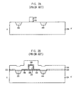
- FIG. 1 is a top view illustrating a layout of a unit cell of a conventional electrically erasable programmable read-only memory (EEPROM).
- EEPROM electrically erasable programmable read-only memory
- the unit cell of the conventional EEPROM includes a floating gate 222 , which is electrically connected.
- the floating gate 222 is formed underneath a polysilicon layer 120 for a control gate.
- FIGS. 2A to 2D are cross-sectional views of the conventional EEPROM of FIG. 1 for illustrating a method for fabricating the same. Particularly, the illustrated conventional EEPROM is cut in the direction of a line A-A′ of FIG. 1 .
- the same reference numerals used in FIG. 1 are used for the same elements described in the following drawings.
- first insulation layers 206 and 208 are formed in a substrate 224 .
- the first insulation layers 206 and 208 are device isolation layers obtained through a shallow trench isolation method. As the name indicates, the first insulation layers 206 and 208 isolate memory cells electrically.
- a silicon oxide layer 230 is formed thinly on a certain region of the substrate 224 .
- a floating gate 222 is formed on the silicon oxide layer 230 .
- a photo-exposure process and a subsequent etching process are performed to complete the formation of the floating gate 222 and then, a third insulation layer including an upper insulation layer 232 and lower insulation layers 236 and 234 is formed over the floating gate 222 .
- Gate oxide layers 202 and 204 are formed in a peripheral region.
- a conductive layer 240 is formed over the above resulting structure.
- the conductive layer 240 is based on a material to be used as an electrode. Metals and semiconductor materials are examples of such electrode material.
- the silicon oxide layer 230 is a gate dielectric layer for the floating gate 222 , and the upper insulation layer 232 and the lower insulation layers 234 and 236 are gate dielectric layers for a select transistor.
- the gate oxide layers 202 and 204 are gate dielectric layers for those transistors formed in the peripheral region.
- a photoresist layer is formed over the conductive layer 240 and photo-exposed to form a first photoresist pattern 250 and a second photoresist pattern 252 .
- the first photoresist pattern 250 is disposed such that each lateral edge of the first photoresist pattern 250 is placed between one outer edge of the upper insulation layer 232 , which encompasses the floating gate 222 , and one sidewall edge of the conductive layer 240 .
- the second photoresist pattern 252 for forming gates is formed in the peripheral region except for a cell region where memory array exists.
- the conductive layer 240 is etched using the first photoresist pattern 250 and the second photoresist pattern 252 as an etch mask.
- the conductive layer 240 is etched in an amount that is higher than the addition of the thickness of the conductive layer 240 and a delta amount taking account of process parameter variations.
- spacers 260 and 262 are formed larger than the first photoresist pattern 250 .
- the spacers 260 and 262 have the same size regardless of a change in the photo-exposure/etching process.
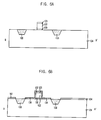
- FIGS. 3A and 3B are cross-sectional views of another conventional split gate type flash memory device with a self-aligned select transistor for illustrating a fabrication method thereof.
- a tunnel oxide layer 12 is formed on a substrate 22 .
- the tunnel oxide layer 12 has a thickness of 85 ⁇ although the typically formed thickness is in a range of 70 ⁇ to 100 ⁇ .
- a first polysilicon layer is formed thereon and is patterned using a photoresist layer, and as a result, a floating gate 14 is obtained.
- the floating gate 14 has a thickness t 3 ranging from 1,000 ⁇ to 3,000 ⁇ .
- An inter-poly-dielectric (IPD) layer 16 is formed over the floating gate 14 and the substrate 22 .
- the IPD layer 16 typically includes an oxide layer, a nitride layer and a combination thereof.
- a second polysilicon layer 18 is formed on the IPD layer 16 .
- the second polysilicon layer 18 has a thickness ranging from 1,500 ⁇ to 4,000 ⁇ .
- a preferable thickness of the second polysilicon layer 18 is 2,500 ⁇ .
- Reference denotations 11 and t 2 represent thicknesses of certain portions of the second polysilicon layer 18 .
- a photoresist layer is formed over the second polysilicon layer 18 and photo-exposed to form a photoresist pattern 20 .
- the edges of the photoresist pattern 20 are disposed in the inward directions X and Y from the sidewalls of the second polysilicon layer 18 .
- the second polysilicon layer 18 is etched using the photoresist pattern 20 as an etch mask.
- An etching amount of the second polysilicon layer 18 is determined based on the addition of the thickness of the second polysilicon layer 18 and an over-etching amount caused by a process margin. Through this etching process, a control gate is formed in a manner to encompass the floating gate 14 and the IPD layer 16 .
- Sidewalls of the control gate act as a gate of a select transistor.
- a plurality of the select transistors are formed with the identical size, and in addition to the illustrated region in FIG. 3B , the select transistors are formed in the identical sizes in other regions as well.
- a poly-slope or a poly-peak is formed due to polymers, which are generated by photoresist patterns 450 and an etchant used in the etching process.
- the above poly-slope or poly-peak generation may become a cause of inducing a salicide-stimulated electric short between a control gate (i.e., the patterned portions of the conductive layer 462 ) and a silicon substrate 424 during a subsequent salicide process.
- salicide is not formed intentionally in the cell region.
- the poly-peak may act as a foreign material, which may further induce product defects.
- control gate When the control gate is doped, a shadow effect appears during the ion implantation process due to the photoresist pattern. Thus, it may be difficult to dope the gates of the select transistors.
- the gate sizes of the select transistors may vary when a misalignment event occurs or a critical dimension is changed due to variations in process parameters or equipment conditions.
- the gate size variation gets severe as the thickness of the second polysilicon layer 18 is decreased.
- the second polysilicon layer 18 gets thinner as semiconductor devices are micronized, it may be difficult to fabricate micronized and integrated devices based on the aforementioned conventional methods.
- an object of the present invention to provide a method for fabricating a non-volatile memory device, wherein spacers of a control gate can be easily formed through an etch-back process instead of a photo-exposure/etching process and a shadow effect does not occur during an ion implantation process for doping the control gate.
- a method for fabricating a non-volatile memory device including: forming a gate structure on a substrate, the gate structure including a first insulation layer, a first electrode layer for a floating gate and a second insulation layer; forming a third insulation layer on the gate structure covering predetermined regions of the substrate adjacent to the gate structure; and forming a second electrode layer for a control gate on the third insulation layer disposed on sidewalls of the gate structure and the predetermined regions of the substrate.
- a method for fabricating a non-volatile memory device including: forming a gate structure for storing data on a first region of a substrate, wherein the gate structure including a first insulation layer, a first electrode layer for a floating gate and a second insulation layer; forming a third insulation layer on the gate structure covering predetermined portions of the first region adjacent to the gate structure; forming a fourth insulation layer on a second region of the substrate; forming a second electrode layer covering the third insulation layer and the fourth insulation layer; forming a photoresist pattern on the fourth insulation layer; and patterning the second electrode layer using the photoresist pattern as an etch mask to form a gate electrode pattern for a peripheral circuit underneath the photoresist pattern and to form an electrode pattern for a control gate on sidewalls of the gate structure.
- a non-volatile memory device including: a plurality of gate structures arranged with a predetermined distance, each gate structure including a first insulation layer, a first electrode layer for a floating gate and a second insulation layer; a plurality of second electrode layers for control gates formed to encompass sidewalls of the individual gate structures; and a plurality of third insulation layers encompassing the respective gate structures such that the individual second electrode layers are apart from the individual gate structures with a predetermined distance.
- a non-volatile memory device including: a first gate structure for storing data, the first gate structure including a first insulation layer, a first electrode layer for a floating gate and a second insulation layer; a third insulation layer formed on the first gate structure covering regions adjacent to a predetermined region contacting the first gate structure; and a second electrode layer for a control gate formed on sidewalls of the third insulation layer.
- FIG. 1 is a top view showing a unit cell layout of a conventional electrically erasable programmable read-only memory (EEPROM);
- EEPROM electrically erasable programmable read-only memory
- FIGS. 2A to 2D are cross-sectional views illustrating a method for fabricating the conventional EEPROM cut in the direction of a line A-A′ shown in FIG. 1 ;
- FIGS. 3A and 3B are cross-sectional views of a conventional split gate type flash memory device with a self-aligned select transistor
- FIG. 4 is a diagram depicting disadvantages of using various types of conventional non-volatile memory devices
- FIG. 5 is a top view showing a unit cell layout of a non-volatile memory device in accordance with an example embodiment of the present invention
- FIGS. 6A to 6D are cross-sectional views of the non-volatile memory device cut in the direction of a line B-B′ of FIG. 5 for illustrating a method for fabricating the same;
- FIG. 7 is a top view showing a layout of a non-volatile memory device obtained after a gate etching process in accordance with an example embodiment of the present invention.
- FIG. 8 is a cross-section view of the non-volatile memory device cut in the direction of a line B-B′ of FIG. 5 where a chip area is covered with salicide.
- FIG. 5 is a top view illustrating a unit memory cell of a non-volatile memory device in accordance with a specific embodiment of the present invention.
- the unit memory cell layout of the non-volatile memory device includes a floating gate 122 without including a polysilicon layer typically used to form a control gate over the floating gate 122 .
- FIGS. 6A to 6D are cross-sectional views of the non-volatile memory device cut in the direction of a line B-B′ of FIG. 5 for illustrating a method for fabricating the same.
- trenches are formed in predetermined regions of a substrate 124 by employing a shallow trench isolation (STI) method and, first insulation layers 106 and 108 are filled into the trenches to isolate memory cells electrically.
- STI shallow trench isolation
- a tunneling oxide layer 130 is formed thinly on the substrate 124 , and a floating gate 122 is formed as an electrode on the tunneling oxide layer 130 .
- the tunneling oxide layer 130 has a preferable thickness ranging from approximately 70 ⁇ to approximately 100 ⁇ .
- a second insulation layer 123 is formed on the floating gate 122 .
- the second insulation layer 123 is used to form a hard mask.
- the floating gate 122 has a thickness ranging from approximately 1,000 ⁇ to approximately 5,000 ⁇ . This thickness of the floating gate 122 should be determined carefully since the thickness is an important factor for determining the coupling ratio of the floating gate 122 .
- the second insulation layer 123 can be one selected from a group consisting of oxide, nitride and a combination thereof.
- a thickness of the second insulation layer 123 is determined by the thickness of the floating gate 122 and, the thickness of the second insulation layer 123 is in a range of approximately 500 ⁇ to approximately 2,000 ⁇ .
- the formation of the floating gate 122 is achieved via a photo-exposure process and an etching process.
- a third insulation layer including an upper insulation layer 132 and lower insulation layers 134 and 136 are formed over the second insulation layer 123 encompassing sidewalls of the floating gate 122 .
- the third insulation layer covers a gate structure, including the floating gate 122 , and active regions located at each side of the gate structures.
- the upper insulation layer 132 and the lower insulation layers 134 and 136 can be formed of a material selected from a group consisting of oxide, nitride and a combination thereof.
- gate insulation layers 102 and 104 are formed on the substrate 124 .
- the thicknesses of the gate insulation layers 102 and 104 are determined by usage of the circuits and devices.
- the gate insulation layers 102 and 104 may have the same or different thicknesses. In the case that the gate insulation layers 102 and 104 have a different thickness, a complex gate insulation process is implemented to form the gate insulation layers 102 and 104 with different thicknesses.
- the conductive layer 140 is an electrode material selected from a group consisting of polysilicon, amorphous silicon (Si), tungsten (W), tungsten silicide (WSi x ), and titanium (Ti).
- a photoresist layer is formed over the conductive layer 140 and photo-exposed to obtain a photoresist pattern 152 .
- the photoresist pattern 152 is not formed in the cell region but in the peripheral region to form a gate for use in a peripheral circuit.
- a control gate can be formed in the cell region without using the photoresist pattern.
- the conductive layer 140 is etched using the photoresist pattern 152 as an etch mask.
- the etching amount of the conductive layer 140 is determined based on the addition of the thickness of the conductive layer 140 and a delta amount taking account of potential variations in related processes.
- spacers 160 and 162 are formed on the active regions locates at each side of the gate structure in the cell region by performing an etch-back process to the conductive layer 140 .
- the spacers 160 and 162 are used as the aforementioned control gate. Sizes of the spacers 160 and 162 are the same because of the etch-back process instead of the conventionally employed photo-exposure process and the etching process, which result in a poly- peak or poly-slope generation.
- a gate electrode 164 is simultaneously formed in the peripheral region.
- FIG. 7 is a top view showing a non-volatile memory device obtained after the above etching process for forming the control gate (i.e., the spacers 160 and 162 ) and the floating gate 122 in accordance with the specific embodiment of the present invention.
- the same reference numerals are used for the same elements described in FIGS. 6A to 6D .
- the floating gates 122 are isolated by the third insulation layers 132 , 134 , and 136 .
- the control gates are formed in the form of sidewall spacers 160 and 162 .
- the spacers 160 and 162 are not disconnected but connected as word lines through being appropriately arranged at a first terminal and a node connected with a bias circuit.
- control gate in the cell region is formed by the etch-back process instead of the conventional photo-exposure process and the etching process.
- spacers for use in the control gate can be easily formed and a shadow effect does not appear during an ion implantation process.
- the implementation of the etch-back process gives a normal shape of the spacers (i.e., no poly-peak or poly-slope event).
- salicide can be applied over the entire chip area, as is shown by salicide layers 170 and 172 in FIG. 8 , thereby reducing word line resistance and contact resistance.
- the decrease in the word line resistance and contact resistance contribute to a smaller chip area. Accordingly, more cost-competitive and stabilized device yields can be achieved.
- control gate Since the control gate does not exist over the floating gate, a height of a memory cell is decreased, thereby further decreasing a height of a contact hole. The decrease in the height of the contact hole can prevent various defect generations.
Landscapes
- Engineering & Computer Science (AREA)
- Manufacturing & Machinery (AREA)
- Semiconductor Memories (AREA)
- Non-Volatile Memory (AREA)
Abstract
Description
Claims (24)
Priority Applications (1)
| Application Number | Priority Date | Filing Date | Title |
|---|---|---|---|
| US12/228,211 US8093631B2 (en) | 2004-10-13 | 2008-08-11 | Non-volatile memory device and method for fabricating the same |
Applications Claiming Priority (3)
| Application Number | Priority Date | Filing Date | Title |
|---|---|---|---|
| US61863504P | 2004-10-13 | 2004-10-13 | |
| US11/250,052 US7425482B2 (en) | 2004-10-13 | 2005-10-12 | Non-volatile memory device and method for fabricating the same |
| US12/228,211 US8093631B2 (en) | 2004-10-13 | 2008-08-11 | Non-volatile memory device and method for fabricating the same |
Related Parent Applications (1)
| Application Number | Title | Priority Date | Filing Date |
|---|---|---|---|
| US11/250,052 Division US7425482B2 (en) | 2004-10-13 | 2005-10-12 | Non-volatile memory device and method for fabricating the same |
Publications (2)
| Publication Number | Publication Date |
|---|---|
| US20080296654A1 US20080296654A1 (en) | 2008-12-04 |
| US8093631B2 true US8093631B2 (en) | 2012-01-10 |
Family
ID=36573211
Family Applications (2)
| Application Number | Title | Priority Date | Filing Date |
|---|---|---|---|
| US11/250,052 Expired - Lifetime US7425482B2 (en) | 2004-10-13 | 2005-10-12 | Non-volatile memory device and method for fabricating the same |
| US12/228,211 Active 2027-03-29 US8093631B2 (en) | 2004-10-13 | 2008-08-11 | Non-volatile memory device and method for fabricating the same |
Family Applications Before (1)
| Application Number | Title | Priority Date | Filing Date |
|---|---|---|---|
| US11/250,052 Expired - Lifetime US7425482B2 (en) | 2004-10-13 | 2005-10-12 | Non-volatile memory device and method for fabricating the same |
Country Status (1)
| Country | Link |
|---|---|
| US (2) | US7425482B2 (en) |
Cited By (2)
| Publication number | Priority date | Publication date | Assignee | Title |
|---|---|---|---|---|
| US8674427B2 (en) | 2011-10-19 | 2014-03-18 | Magnachip Semiconductor, Ltd. | Nonvolatile memory device and method of manufacturing thereof |
| US20190123059A1 (en) * | 2017-10-19 | 2019-04-25 | Globalfoundries Singapore Pte. Ltd. | Integrated circuits with memory cells and method for producing the same |
Families Citing this family (7)
| Publication number | Priority date | Publication date | Assignee | Title |
|---|---|---|---|---|
| KR100642384B1 (en) * | 2005-09-15 | 2006-11-03 | 주식회사 하이닉스반도체 | Transistor of semiconductor memory device and manufacturing method thereof |
| US8809179B2 (en) * | 2006-04-13 | 2014-08-19 | Taiwan Semiconductor Manufacturing Company, Ltd. | Method for reducing topography of non-volatile memory and resulting memory cells |
| KR100843055B1 (en) * | 2006-08-17 | 2008-07-01 | 주식회사 하이닉스반도체 | Flash memory device and manufacturing method thereof |
| KR101024336B1 (en) * | 2009-02-13 | 2011-03-23 | 매그나칩 반도체 유한회사 | Nonvolatile Memory Cells and Manufacturing Method Thereof |
| US8836006B2 (en) * | 2012-12-14 | 2014-09-16 | Spansion Llc | Integrated circuits with non-volatile memory and methods for manufacture |
| US10446563B1 (en) * | 2018-04-04 | 2019-10-15 | Texas Instruments Incorporated | Partially disposed gate layer into the trenches |
| KR102274881B1 (en) | 2019-07-05 | 2021-07-07 | 주식회사 키 파운드리 | Non volatile memory device |
Citations (12)
| Publication number | Priority date | Publication date | Assignee | Title |
|---|---|---|---|---|
| US5414286A (en) * | 1992-03-19 | 1995-05-09 | Sharp Kabushiki Kaisha | Nonvolatile memory, method of fabricating the same, and method of reading information from the same |
| US5981364A (en) * | 1995-12-06 | 1999-11-09 | Advanced Micro Devices, Inc. | Method of forming a silicon gate to produce silicon devices with improved performance |
| US6452226B2 (en) * | 1998-11-10 | 2002-09-17 | Mitsubishi Denki Kabushiki Kaisha | Non-volatile semiconductor memory device and manufacturing method thereof |
| US6451652B1 (en) * | 1999-09-15 | 2002-09-17 | The John Millard And Pamela Ann Caywood 1989 Revocable Living Trust | Method for forming an EEPROM cell together with transistor for peripheral circuits |
| US20030198086A1 (en) * | 2002-04-18 | 2003-10-23 | Shoji Shukuri | Semiconductor integrated circuit device and a method of manufacturing the same |
| US6686632B2 (en) * | 1999-10-25 | 2004-02-03 | New Halo, Inc. | Dual-bit multi-level ballistic MONOS memory |
| US20040026748A1 (en) * | 2002-06-06 | 2004-02-12 | Akira Goda | Semiconductor device with source line and fabrication method thereof |
| US20040151028A1 (en) * | 2003-01-31 | 2004-08-05 | Taiwan Semiconductor Manufacturing Company | Memory array and its peripheral circuit with byte-erase capability |
| US20040191993A1 (en) * | 2001-11-30 | 2004-09-30 | Renesas Technology Corp. | Nonvolatile semiconductor memory device and manufacturing method thereof |
| US20050117419A1 (en) * | 2003-11-28 | 2005-06-02 | Sharp Kabushiki Kaisha | Method of evaluating characteristics of semiconductor memory element, and method of extracting model parameter of semiconductor memory element |
| US6979617B2 (en) * | 2004-04-30 | 2005-12-27 | Anam Semiconductor Ltd. | Method for fabricating flash memory device |
| US7183662B2 (en) * | 2003-08-23 | 2007-02-27 | Samsung Electronics Co., Ltd. | Memory devices with memory cell transistors having gate sidewell spacers with different dielectric properties |
-
2005
- 2005-10-12 US US11/250,052 patent/US7425482B2/en not_active Expired - Lifetime
-
2008
- 2008-08-11 US US12/228,211 patent/US8093631B2/en active Active
Patent Citations (12)
| Publication number | Priority date | Publication date | Assignee | Title |
|---|---|---|---|---|
| US5414286A (en) * | 1992-03-19 | 1995-05-09 | Sharp Kabushiki Kaisha | Nonvolatile memory, method of fabricating the same, and method of reading information from the same |
| US5981364A (en) * | 1995-12-06 | 1999-11-09 | Advanced Micro Devices, Inc. | Method of forming a silicon gate to produce silicon devices with improved performance |
| US6452226B2 (en) * | 1998-11-10 | 2002-09-17 | Mitsubishi Denki Kabushiki Kaisha | Non-volatile semiconductor memory device and manufacturing method thereof |
| US6451652B1 (en) * | 1999-09-15 | 2002-09-17 | The John Millard And Pamela Ann Caywood 1989 Revocable Living Trust | Method for forming an EEPROM cell together with transistor for peripheral circuits |
| US6686632B2 (en) * | 1999-10-25 | 2004-02-03 | New Halo, Inc. | Dual-bit multi-level ballistic MONOS memory |
| US20040191993A1 (en) * | 2001-11-30 | 2004-09-30 | Renesas Technology Corp. | Nonvolatile semiconductor memory device and manufacturing method thereof |
| US20030198086A1 (en) * | 2002-04-18 | 2003-10-23 | Shoji Shukuri | Semiconductor integrated circuit device and a method of manufacturing the same |
| US20040026748A1 (en) * | 2002-06-06 | 2004-02-12 | Akira Goda | Semiconductor device with source line and fabrication method thereof |
| US20040151028A1 (en) * | 2003-01-31 | 2004-08-05 | Taiwan Semiconductor Manufacturing Company | Memory array and its peripheral circuit with byte-erase capability |
| US7183662B2 (en) * | 2003-08-23 | 2007-02-27 | Samsung Electronics Co., Ltd. | Memory devices with memory cell transistors having gate sidewell spacers with different dielectric properties |
| US20050117419A1 (en) * | 2003-11-28 | 2005-06-02 | Sharp Kabushiki Kaisha | Method of evaluating characteristics of semiconductor memory element, and method of extracting model parameter of semiconductor memory element |
| US6979617B2 (en) * | 2004-04-30 | 2005-12-27 | Anam Semiconductor Ltd. | Method for fabricating flash memory device |
Cited By (3)
| Publication number | Priority date | Publication date | Assignee | Title |
|---|---|---|---|---|
| US8674427B2 (en) | 2011-10-19 | 2014-03-18 | Magnachip Semiconductor, Ltd. | Nonvolatile memory device and method of manufacturing thereof |
| US20190123059A1 (en) * | 2017-10-19 | 2019-04-25 | Globalfoundries Singapore Pte. Ltd. | Integrated circuits with memory cells and method for producing the same |
| US10411027B2 (en) * | 2017-10-19 | 2019-09-10 | Globalfoundries Singapore Pte. Ltd. | Integrated circuits with memory cells and method for producing the same |
Also Published As
| Publication number | Publication date |
|---|---|
| US20060118857A1 (en) | 2006-06-08 |
| US20080296654A1 (en) | 2008-12-04 |
| US7425482B2 (en) | 2008-09-16 |
Similar Documents
| Publication | Publication Date | Title |
|---|---|---|
| US8093631B2 (en) | Non-volatile memory device and method for fabricating the same | |
| US7436017B2 (en) | Semiconductor integrated circuit using a selective disposable spacer | |
| US7518915B2 (en) | Nonvolatile semiconductor storage device | |
| JP4086790B2 (en) | Nonvolatile memory and manufacturing method thereof | |
| US7061040B2 (en) | Memory device | |
| US6821849B2 (en) | Split gate flash memory cell and manufacturing method thereof | |
| US6794710B2 (en) | Split-gate flash memory structure and method of manufacture | |
| US7928494B2 (en) | Semiconductor device | |
| US8198662B2 (en) | Semiconductor memory device and method of manufacturing the same | |
| US6867099B2 (en) | Spilt-gate flash memory structure and method of manufacture | |
| KR100538075B1 (en) | Method of manufacturing a flash memory device | |
| JP2002141425A (en) | Sidewall process to improve flash memory cell performance | |
| KR100931494B1 (en) | Non-volatile memory device manufacturing method | |
| US6905930B2 (en) | Memory device and fabrication method thereof | |
| KR20040019191A (en) | Manufacturing method for flash memory device | |
| US6943119B2 (en) | Flash process for stacking poly etching | |
| KR100671615B1 (en) | Manufacturing Method of NAND Flash Memory Device | |
| US20080197402A1 (en) | Methods of Forming Nonvolatile Memory Devices and Memory Devices Formed Thereby | |
| KR100719738B1 (en) | Flash memory device and method of operating and manufacturing the same | |
| JP2004087843A (en) | Semiconductor device | |
| US20050247987A1 (en) | Flash memory device and method for fabricating the same | |
| KR20050112990A (en) | Method of manufacturing nand flash memory device | |
| KR20050002416A (en) | Method of manufacturing flash memory device | |
| KR20060066961A (en) | NAND type nonvolatile memory device and method of forming the same |
Legal Events
| Date | Code | Title | Description |
|---|---|---|---|
| AS | Assignment |
Owner name: U.S. BANK NATIONAL ASSOCIATION, AS COLLATERAL TRUS Free format text: AFTER-ACQUIRED INTELLECTUAL PROPERTY KUN-PLEDGE AGREEMENT;ASSIGNOR:MAGNACHIP SEMICONDUCTOR, LTD.;REEL/FRAME:022277/0133 Effective date: 20090217 |
|
| FEPP | Fee payment procedure |
Free format text: PAYOR NUMBER ASSIGNED (ORIGINAL EVENT CODE: ASPN); ENTITY STATUS OF PATENT OWNER: LARGE ENTITY |
|
| STCF | Information on status: patent grant |
Free format text: PATENTED CASE |
|
| AS | Assignment |
Owner name: MAGNACHIP SEMICONDUCTOR LTD., KOREA, REPUBLIC OF Free format text: RELEASE BY SECURED PARTY;ASSIGNOR:U.S. BANK NATIONAL ASSOCIATION;REEL/FRAME:030988/0419 Effective date: 20100527 |
|
| FPAY | Fee payment |
Year of fee payment: 4 |
|
| MAFP | Maintenance fee payment |
Free format text: PAYMENT OF MAINTENANCE FEE, 8TH YEAR, LARGE ENTITY (ORIGINAL EVENT CODE: M1552); ENTITY STATUS OF PATENT OWNER: LARGE ENTITY Year of fee payment: 8 |
|
| AS | Assignment |
Owner name: KEY FOUNDRY CO., LTD., KOREA, REPUBLIC OF Free format text: ASSIGNMENT OF ASSIGNORS INTEREST;ASSIGNOR:MAGNACHIP SEMICONDUCTOR, LTD.;REEL/FRAME:053703/0227 Effective date: 20200828 |
|
| MAFP | Maintenance fee payment |
Free format text: PAYMENT OF MAINTENANCE FEE, 12TH YEAR, LARGE ENTITY (ORIGINAL EVENT CODE: M1553); ENTITY STATUS OF PATENT OWNER: LARGE ENTITY Year of fee payment: 12 |
|
| AS | Assignment |
Owner name: MAGNACHIP SEMICONDUCTOR, LTD., KOREA, REPUBLIC OF Free format text: ASSIGNMENT OF ASSIGNORS INTEREST;ASSIGNOR:JEONG, YONG-SIK;REEL/FRAME:066543/0347 Effective date: 20060104 |
|
| AS | Assignment |
Owner name: SK KEYFOUNDRY INC., KOREA, REPUBLIC OF Free format text: CHANGE OF NAME;ASSIGNOR:KEY FOUNDRY CO., LTD.;REEL/FRAME:066794/0290 Effective date: 20240130 |