US8090052B2 - Systems and methods for digital delayed array transmitter architecture with beam steering capability for high data rate - Google Patents
Systems and methods for digital delayed array transmitter architecture with beam steering capability for high data rate Download PDFInfo
- Publication number
- US8090052B2 US8090052B2 US11/729,588 US72958807A US8090052B2 US 8090052 B2 US8090052 B2 US 8090052B2 US 72958807 A US72958807 A US 72958807A US 8090052 B2 US8090052 B2 US 8090052B2
- Authority
- US
- United States
- Prior art keywords
- delay
- digital
- signal
- analog converter
- modulator
- Prior art date
- Legal status (The legal status is an assumption and is not a legal conclusion. Google has not performed a legal analysis and makes no representation as to the accuracy of the status listed.)
- Expired - Fee Related, expires
Links
Images


Classifications
-
- H—ELECTRICITY
- H01—ELECTRIC ELEMENTS
- H01Q—ANTENNAS, i.e. RADIO AERIALS
- H01Q3/00—Arrangements for changing or varying the orientation or the shape of the directional pattern of the waves radiated from an antenna or antenna system
- H01Q3/26—Arrangements for changing or varying the orientation or the shape of the directional pattern of the waves radiated from an antenna or antenna system varying the relative phase or relative amplitude of energisation between two or more active radiating elements; varying the distribution of energy across a radiating aperture
- H01Q3/2682—Time delay steered arrays
Definitions
- the present invention is in the field of wireless communications between a host computing system and multiple endpoint devices. More particularly, the invention is in the field of management of remote pipe resources in a wireless adapter.
- Wireless computing is a term that has come to describe wireless communications between computing devices or between a computer and peripheral devices such as printers.
- many computers including tower and laptop models, have a wireless communications card that comprises a transmitter and receiver connected to an antenna.
- a Host Wire Adapter (HWA) is connected to the computer by a USB (Universal Serial Bus) cable.
- the HWA has an RF (Radio Frequency) transmitter and receiver capable of communicating data in a USB-cognizable format. This enables the computer to communicate by RF transmission with a wireless network of computers and peripheral devices.
- the flexibility and mobility that wireless computing affords is a major reason for its commercial success.
- multiple-antennas can be used, together with delay elements or phase shifters in multiple TX paths, to form the required beam.
- Phase-shifting the local oscillator (LO) signal between multiple TX paths or Cartesian combining of multiple TX paths has been used in implementing phased-array systems, with the limitation of narrow-band operation.
- EVM error vector magnitude
- FIG. 1 depicts an embodiment of a computer to control aperture control shutters and to communicate with peripheral devices.
- FIG. 2 depicts a transceiver in a computer-based communications system.
- FIG. 3 depicts a phased array architecture
- FIG. 4 depicts an embodiment of a digitally delayed transmit (TX) architecture.
- FIG. 5 depicts an embodiment of delay locked loop digital delay architecture.
- FIG. 6 depicts an embodiment of digital delay based TX architecture.
- Embodiments include systems and methods for fine control of beam steering for wide band wireless applications using a phased array of antenna elements.
- a digitally controlled delay line delays the signal output from a modulator in each branch of multiple branches feeding multiple antennas in an array.
- An output of the digital delay line is input to a digital to analog converter.
- a second digital delay line also delays the signal within the digital to analog converter. The manner of implementation of the delays enables accurate production of a steered beam at a high data rate.
- the wireless communication systems described herein are intended to represent any of a wide variety of wireless systems which may include without limitation, NFC (Near Field Communications), WPAN (Wireless Personal Area Network), WLAN (Wireless Local Area Network), WMAN (Wireless Metropolitan Area Network), WiMAX (Worldwide Interoperability for Microwave Access), 2.5-3G (Generation) cellular, 3G RAN (Radio Access Network), 4G, RFID (Radio Frequency Identification), etc.
- NFC Near Field Communications
- WPAN Wireless Personal Area Network
- WLAN Wireless Local Area Network
- WMAN Wireless Metropolitan Area Network
- WiMAX Worldwide Interoperability for Microwave Access
- 2.5-3G Geneeration
- 3G RAN Radio Access Network
- 4G Radio Frequency Identification
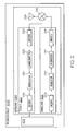
- FIG. 1 shows a view of a computer 100 of a host system to communicate with wireless devices.
- Computer 100 comprises a system memory 110 , a memory controller 120 , an L2 cache 130 , and a processor 140 .
- System memory 110 comprises a hard disk drive memory, Read-Only Memory (ROM), and Random Access Memory (RAM).
- System memory 110 stores antenna phase shift control code 112 , Operating System (OS) code 114 , Basic Input-Output System (BIOS) code (not shown), and code for other application programs 116 .
- System memory 110 also stores data and files 118 .
- the antenna phase shift control code 112 , OS code 114 , and applications code 116 are typically stored on a hard drive, whereas BIOS code is typically stored in ROM.
- Memory controller 120 effectuates transfers of instructions and data from system memory 110 to L2 cache 130 and from L2 cache 130 to an L1 cache 144 of processor 140 .
- data and instructions are transferred from a hard drive to L2 cache near the time when they will be needed for execution in processor 140 .
- L2 cache 130 is fast memory located physically close to processor 140 . Instructions may include load and store instructions, branch instructions, arithmetic logic instructions, floating point instructions, etc.
- L1 cache 144 is located in processor 140 and contains data and instructions received from L2 cache 130 . Ideally, as the time approaches for a program instruction to be executed, the instruction is passed with its data, if any, first to the L2 cache, and then as execution time is near imminent, to the L1 cache.
- processor 140 also comprises an instruction fetcher 142 , instruction decoder 146 , instruction buffer 148 , a dispatch unit 150 , execution units 152 and control circuitry 154 .
- Instruction fetcher 142 fetches instructions from memory.
- Instruction fetcher 142 maintains a program counter and fetches instructions from L1 cache 130 .
- the program counter of instruction fetcher 142 comprises an address of a next instruction to be executed.
- Instruction fetcher 142 also performs pre-fetch operations.
- instruction fetcher 142 communicates with a memory controller 214 to initiate a transfer of instructions from the system memory 110 , to instruction cache L2 130 , and to L1 instruction cache 144 .
- the place in the cache to where an instruction is transferred from system memory 110 is determined by an index obtained from the system memory address.
- Instruction fetcher 142 retrieves instructions passed to instruction cache 144 and passes them to an instruction decoder 146 .
- Instruction decoder 146 receives and decodes the instructions fetched by instruction fetcher 142 .
- An instruction buffer 148 receives the decoded instructions from instruction decoder 146 .
- Instruction buffer 148 comprises memory locations for a plurality of instructions. Instruction buffer 148 may reorder the order of execution of instructions received from instruction decoder 146 . Instruction buffer 148 therefore comprises an instruction queue to provide an order in which instructions are sent to a dispatch unit 150 .
- Dispatch unit 150 dispatches instructions received from instruction buffer 148 to execution units 152 .
- execution units 152 may comprise load/store units, integer Arithmetic/Logic Units, floating point Arithmetic/Logic Units, and Graphical Logic Units, all operating in parallel.
- Dispatch unit 150 therefore dispatches instructions to some or all of the executions units to execute the instructions simultaneously.
- Execution units 152 comprise stages to perform steps in the execution of instructions received from dispatch unit 150 .
- Data processed by execution units 152 are storable in and accessible from integer register files and floating point register files not shown. Thus, instructions are executed sequentially and in parallel.
- FIG. 1 also shows control circuitry 154 to perform a variety of functions that control the operation of processor 100 .
- an operation controller within control circuitry 154 interprets the OPCode contained in an instruction and directs the appropriate execution unit to perform the indicated operation.
- control circuitry 154 may comprise a branch redirect unit to redirect instruction fetcher 142 when a branch is determined to have been mispredicted.
- Control circuitry 154 may further comprise a flush controller to flush instructions younger than a mispredicted branch instruction.
- Computer 100 further comprises other components and systems not shown in FIG. 1 , including, RAM, peripheral drivers, a system monitor, a keyboard, flexible diskette drives, removable non-volatile media drives, CD and DVD drives, a pointing device such as a mouse, etc.
- Computer 100 may be a personal computer, a workstation, a server, a mainframe computer, a notebook or laptop computer, etc.
- FIG. 2 shows an embodiment of an integrated circuit 1002 comprising a transceiver unit 1024 as may be found in a wireless computing system.
- Transceiver 1024 comprises a receiver 204 and a transmitter 206 .
- An embodiment of a transmitter comprises an encoder 208 , a modulator 210 , an upconverter 212 , and an amplification, stage 214 .
- An embodiment of a receiver comprises an amplification stage 220 , a downconverter 222 , a demodulator 224 and a decoder 226 .
- Encoder 208 of transmitter 206 receives data destined for transmission from a core 202 .
- Core 202 may comprise a computing system such as described with reference to FIG. 1 .
- Core 202 presents data to transceiver 1024 in blocks such as bytes of data and receives data from transceiver 1024 .
- Encoder 208 encodes the data and may introduce redundancy to the data stream.
- Encoding may be done to achieve one or more of a plurality of different purposes. For example, coding may be performed to decrease the average number of bits that must be sent to transfer each symbol of information to be transmitted. Coding may be performed to decrease a probability of error in symbol detection at the receiver. Thus, an encoder may introduce redundancy to the data stream.
- Adding redundancy increases the channel bandwidth required to transmit the information, but results in less error, and enables the signal to be transmitted at lower power. Adding redundancy increases the channel bandwidth required to transmit the information, but results in less error, and enables the signal to be transmitted at lower power. Encryption may also be performed for security.
- One type of encoding is block encoding.
- the encoder encodes a block of k information bits into corresponding blocks of n code bits, where n is greater than k.
- An example of a block encoder that can be implemented is a Reed-Solomon encoder, known by those skilled in the art of encoding.
- Another type of encoding is linear convolutional encoding.
- the convolutional encoder may be viewed as a linear finite-state shift register with an output sequence comprising a set of linear combinations of the input sequence. The number of output bits from the shift register for each input bit is a measure of the redundancy in the code.
- different embodiments may implement different encoding algorithms.
- Modulator 210 of transmitter 206 receives data from encoder 208 .
- a purpose of modulator 210 is to transform each block of binary data received from encoder 208 into a unique continuous-time waveform that can be transmitted by an antenna upon upconversion and amplification.
- the modulator impresses the received data blocks onto a sinusoid of a selected frequency.
- the output of the modulator is a band pass signal that is upconverted to a transmission frequency, amplified, and delivered to an antenna.
- modulator 210 maps a sequence of binary digits into a set of discrete amplitudes of a carrier frequency. This is called Pulse Amplitude Modulation (PAM). Quadrature Amplitude Modulation (QAM) is attained by impressing two separate k-bit symbols from the information sequence onto two quadrature frequencies, cos (2 ⁇ ft) and sin(2 ⁇ ft).
- PAM Pulse Amplitude Modulation
- QAM Quadrature Amplitude Modulation
- modulator 210 maps the blocks of data received from encoder 208 into a set of discrete phases of the carrier to produce a Phase-Shift Keyed (PSK) signal.
- PSK Phase-Shift Keyed
- a resulting equivalent low pass signal may be represented as
- g(t ⁇ nT) is a basic pulse whose shape may be optimized to increase the probability of accurate detection at a receiver by, for example, reducing inter-symbol interference.
- Inter-symbol interference results when the channel distorts the pulses. When this occurs adjacent pulses are smeared to the point that individual pulses are difficult to distinguish.
- a pulse shape may therefore be selected to reduce the probability of symbol misdetection due to inter-symbol interference.
- modulator 210 maps the blocks of data from an information sequence received from encoder 208 into a set of discrete frequency shifts to produce a Frequency-Shift-Keyed (FSK) signal.
- FSK Frequency-Shift-Keyed
- I n is an odd integer up to N ⁇ 1
- ⁇ f is a unit of frequency shift.
- the output of modulator 210 is fed to upconverter 212 .
- a purpose of upconverter 212 is to shift the modulated waveform received from modulator 210 to a much higher frequency. Shifting the signal to a much higher frequency before transmission enables use of an antenna of practical dimensions. That is, the higher the transmission frequency, the smaller the antenna can be.
- an up-converter multiplies the modulated waveform by a sinusoid to obtain a signal with a carrier frequency that is the sum of the central frequency of the waveform and the frequency of the sinusoid. The operation is based on the trigonometric identity:
- the required bandwidth of the transmitted signal depends upon the method of modulation. A bandwidth of about 10% is exemplary.
- the encoded, modulated, upconverted, filtered signal is passed to amplifier 214 .
- amplifier 214 provides high power amplification to drive the antenna 218 .
- the power does not need to be very high to be received by receivers in close proximity to transmitter 206 .
- one may implement a transmitter of moderate or low power output capacity.
- the required RF transmitter power to effectuate communications within the distances between transceiver units and an endpoint device may be varied.
- FIG. 2 also shows diplexers 216 connected to antenna system 218 .
- the antenna system comprises an array of antenna elements for transmitting highly directive antenna beams.
- the signal from amplifier 214 passes through diplexer 216 and drives the antenna with the upconverted information-bearing signal.
- the diplexer prevents the signal from amplifier 214 from entering receiver 204 .
- an information bearing signal received by the antenna passes through diplexer 216 to deliver the signal from the antenna to receiver 204 .
- the diplexer then prevents the received signal from entering transmitter 206 .
- separate antennas may be used for transmit and receive and a diplexer is not needed.
- a transmit antenna 218 radiates the information bearing signal into a time-varying, spatial distribution of electromagnetic energy that can be received by an antenna of a receiver.
- FIG. 2 also shows an embodiment of a receiver 204 for receiving, demodulating, and decoding an information bearing signal.
- the signal is fed from antenna 218 to a low noise amplifier 220 .
- Amplifier 220 comprises filter circuitry which passes the desired signal information and filters out noise and unwanted signals at frequencies outside the pass band of the filter circuitry.
- a downconverter 222 downconverts the signal at the carrier frequency to an intermediate frequency or to base band. By shifting the received signal to a lower frequency or to baseband, the function of demodulation is easier to perform.
- Demodulator 224 demodulates the received signal to extract the information content from the received down converted signal to produce an information signal.
- Decoder 226 decodes the information signal received from demodulator 224 and transmits the decoded information to core 202 .
- a transceiver will comprise numerous additional components not shown in FIG. 2 . Note that each endpoint device has its own transceiver which operates substantially as described above.
- a delayed-array system consists of several signal paths connected to separate antennas as shown in FIG. 3 .
- Each antenna element 302 of an antenna array receives a signal from a power amplifier 304 .
- the signal input to a power amplifier is delayed by a delay element 306 .
- This system of FIG. 3 can imitate a directional antenna, with digitally controlled angle of radiation.
- the amount of delay in each signal path determines the direction in which the signals add constructively (coherent addition), achieving maximum composite radiated power. In other directions, the signals add destructively (incoherent addition), resulting in lower composite radiated power in these directions.
- the total directed power equals n 2 P s , where P s is the power radiated by one path.
- angle of radiation ⁇ distance between antennas d, delay between two adjacent antennas ⁇ , speed of light c, operating frequency ⁇ 0 , and wavelength ⁇ 0 ; then we can calculate ⁇ as:
- FIG. 4 shows a diagram of a proposed architecture, showing the added programmable variable delay elements 402 , 404 , and 406 .
- This architecture implements the broad band gain equation:
- G ⁇ ( ⁇ ) sin 2 ( ⁇ ⁇ ⁇ n ⁇ d ⁇ 0 ⁇ ( sin ⁇ ( ⁇ ) - sin ⁇ ( ⁇ ) ) ) n 2 ⁇ sin 2 ( ⁇ ⁇ d ⁇ 0 ⁇ ( sin ⁇ ( ⁇ ) - sin ⁇ ( ⁇ ) ) )
- the delay is based on using inverters, delay must be added in the LO and the digital part of the TX.
- the signal is converted to analog form in the semi-digital DAC/Filter block 408 .
- the programmable delay elements 404 and 402 are added at the input of the DAC and in the LO path, where there is no amplitude information. In this way, one can avoid inserting the inverter-based delays at the output of the DAC where the signal is in analog form and has amplitude variations.
- FIG. 5 An implementation of a digitally programmable delay block is shown in FIG. 5 .
- the delay has to be on the order of an inverter delay (10 ps to 20 ps), to give an acceptable beam steering resolution.
- This delay can be stabilized through a delay-locked loop (DLL) to compensate for process and temperature variations.
- FIG. 5 shows a simple DLL with a phase-detector (PD) and a low-pass filter (LPF) 504 to adjust the delay of each inverter 502 . If fine beam steering is required, then fine delay is required which can be achieved by using a delay vernier technique.
- PD phase-detector
- LPF low-pass filter
- Embodiments include a system for beam steering in a wide band wireless system.
- Embodiments comprise a modulator to output an information bearing digital signal, to a plurality of branches, each branch leading to an antenna in array of antennas.
- the system comprises a controllable delay line of inverters to controllably delay the digital signal received from the modulator and passing the signal to a digital to analog converter.
- the system further comprises a controllable delay line of inverters to delay the digital signal processed by the digital to analog converter to achieve beam steering with substantially small error when transmitting a wide band signal.
- the system may further comprise delay circuitry to delay an analog signal output by the digital to analog converter.
- a controllable delay line comprises a delay locked loop.
- the delay implemented by an inverter may be on the order of tens of pico-seconds.
- a controllable delay is implemented by programmable control of a number of inverters in the delay line.
- FIG. 6 shows another embodiment.
- a clock source (at the desired RF frequency) drives tapped digital delay lines 602 .
- Each delay line consists of unit elements whose intrinsic delay is much smaller than one clock period and synthesizes multiple phases of the input clock waveform.
- One phase from each delay line is selected by a multiplexer 604 .
- the selection control for the delay lines are driven by a block that digitally decomposes the desired baseband signal into the outphasing components. Since each delay line only consists of discrete phases, a sigma-delta modulator 606 that dithers between these discrete values can be used to realize a finer average phase.
- the programmable delay elements for beam-steering are added to the multiple transmit paths.
- Embodiments enable beam steering for wide band signals in wireless applications where antenna gain is directed toward a controllable angle of radiation.
- the EVM Error Vector Magnitude
- Embodiments provide for reconfiguration for multi-mode operation, scalability, smaller die area, lower power consumption, with less sensitivity to process and temperature.
- the techniques described herein facilitate the integration of small CMOS PA (Power Amplifier) modules into the RFIC (Radio Frequency Integrated Circuit). PA integration in advanced CMOS processes becomes more reliable as each PA module can use lower supply voltage and avoids problems of break-down and hot-carrier effects.
- the technique is based on digital electronic control for steering the beam or radiation angle.
- a TX designed according to the methods described herein can be used both for MIMO (Multiple Input Multiple Output) or beam steering, so there is no need to use separate antennas for beam steering in a MIMO system. Rather, the system can be used for both techniques simultaneously if more antennas are used. The techniques can also be used for interference cancellation as the output radiated power is minimized in other directions different than the selected beam steered angle.
- MIMO Multiple Input Multiple Output
- beam steering so there is no need to use separate antennas for beam steering in a MIMO system. Rather, the system can be used for both techniques simultaneously if more antennas are used.
- the techniques can also be used for interference cancellation as the output radiated power is minimized in other directions different than the selected beam steered angle.
Landscapes
- Radio Transmission System (AREA)
Abstract
Description
where g(t−nT) is a basic pulse whose shape may be optimized to increase the probability of accurate detection at a receiver by, for example, reducing inter-symbol interference. Inter-symbol interference results when the channel distorts the pulses. When this occurs adjacent pulses are smeared to the point that individual pulses are difficult to distinguish. A pulse shape may therefore be selected to reduce the probability of symbol misdetection due to inter-symbol interference.
where In is an odd integer up to N−1 and Δf is a unit of frequency shift. Thus, in an FSK signal, each symbol of an information sequence is mapped into one of N frequency shifts.
The signal at the sum frequency (A+B) is passed and the signal at the difference frequency (A−B) is filtered out. Thus, a band pass filter is provided to ideally filter out all but the information to be transmitted, centered at the carrier (sum) frequency.
Therefore, the delay from the m-th antenna equals mτ. If we add a delay in the m-th signal path of −mτ; then all the radiated signals will add constructively. This is equivalent to adding zero delay in the longest path and nτ delay in the shortest path (where n is the total number of paths). This can be written as a function of the input signal Sin(t) as:
For a modulated signal Sin(t), the delay in each path will affect both amplitude and phase modulation. If the amplitude and phase modulation are represented as A(t) and φ(t), then:
S in(t)=A(t)exp(j(ω0 t+φ(t)))
is the input signal and
S in(t−mτ)=A(t−mτ)exp(j(ω0 t−mω 0τ+φ(t−mτ)))
is delayed signal in one path. For narrow-band modulated signal, the amplitude and phase modulation are varying slowly relative to the carrier frequency, and therefore this delayed signal can be approximated by:
S in(t−mτ)≈A(t)exp(j(ω0 t−mω 0τ+φ(t)))=S in(t)exp(−jmω 0τ)
-
- a) One for narrow-band signaling by using Cartesian signal representation and combining or dealing with phase shifts in each path, e.g., multiple LO (local oscillator) phase shift techniques found in the literature which are used in implementing phased-array RX (receive) and TX (transmit) systems using a complex LO “bus” with beam steering accuracy being a function of the number of LO phases.
- b) The other is more general and suitable for wide-band applications (in which case one must contend with time delays in each path).
Claims (20)
Priority Applications (1)
| Application Number | Priority Date | Filing Date | Title |
|---|---|---|---|
| US11/729,588 US8090052B2 (en) | 2007-03-29 | 2007-03-29 | Systems and methods for digital delayed array transmitter architecture with beam steering capability for high data rate |
Applications Claiming Priority (1)
| Application Number | Priority Date | Filing Date | Title |
|---|---|---|---|
| US11/729,588 US8090052B2 (en) | 2007-03-29 | 2007-03-29 | Systems and methods for digital delayed array transmitter architecture with beam steering capability for high data rate |
Publications (2)
| Publication Number | Publication Date |
|---|---|
| US20080240170A1 US20080240170A1 (en) | 2008-10-02 |
| US8090052B2 true US8090052B2 (en) | 2012-01-03 |
Family
ID=39794243
Family Applications (1)
| Application Number | Title | Priority Date | Filing Date |
|---|---|---|---|
| US11/729,588 Expired - Fee Related US8090052B2 (en) | 2007-03-29 | 2007-03-29 | Systems and methods for digital delayed array transmitter architecture with beam steering capability for high data rate |
Country Status (1)
| Country | Link |
|---|---|
| US (1) | US8090052B2 (en) |
Cited By (4)
| Publication number | Priority date | Publication date | Assignee | Title |
|---|---|---|---|---|
| US20130127667A1 (en) * | 2010-01-15 | 2013-05-23 | Martin Schneider | Imaging system |
| US9577690B2 (en) | 2007-05-23 | 2017-02-21 | Hypres, Inc. | Wideband digital spectrometer |
| CN108303689A (en) * | 2018-01-19 | 2018-07-20 | 浙江大学 | A kind of device of light-operated radar array dynamic reconfigurable and difference beam |
| US10768216B2 (en) | 2018-03-15 | 2020-09-08 | Rohde & Schwarz Gmbh & Co. Kg | Test arrangement and test method |
Families Citing this family (9)
| Publication number | Priority date | Publication date | Assignee | Title |
|---|---|---|---|---|
| US7756471B2 (en) * | 2007-03-31 | 2010-07-13 | Intel Corporation | Systems and methods for multi-element antenna arrays with aperture control shutters |
| US20130076424A1 (en) | 2011-09-23 | 2013-03-28 | Qualcomm Incorporated | System and method for reducing cross coupling effects |
| US8831158B2 (en) | 2012-03-29 | 2014-09-09 | Broadcom Corporation | Synchronous mode tracking of multipath signals |
| IL231163A (en) * | 2014-02-26 | 2016-05-31 | Elta Systems Ltd | System and method for enhancing dynamic range of a beamforming multi-channel digital receiver |
| EP3300256B1 (en) | 2016-09-27 | 2021-06-02 | Rohde & Schwarz GmbH & Co. KG | Method for controlling digital-to-analogue converters and rf transmit circuit arrangement |
| JPWO2018061899A1 (en) * | 2016-09-28 | 2019-07-18 | 日本電気株式会社 | Transmitter and control method of transmitter |
| IL257059B (en) | 2018-01-21 | 2019-03-31 | Satixfy Uk Ltd | Multi-beamforming system and method |
| KR20210057416A (en) * | 2019-11-12 | 2021-05-21 | 삼성전자주식회사 | Wireless communication device and method |
| US20230379826A1 (en) * | 2022-05-17 | 2023-11-23 | Qualcomm Incorporated | Narrowband component carrier for low power user equipment |
Citations (16)
| Publication number | Priority date | Publication date | Assignee | Title |
|---|---|---|---|---|
| US5861845A (en) * | 1998-05-19 | 1999-01-19 | Hughes Electronics Corporation | Wideband phased array antennas and methods |
| US5943010A (en) * | 1997-01-21 | 1999-08-24 | Ail Systems, Inc. | Direct digital synthesizer driven phased array antenna |
| US20020013133A1 (en) * | 1999-05-18 | 2002-01-31 | Larry K. Lam | Mixed signal true time delay digital beamformer |
| US20020109629A1 (en) * | 2000-01-07 | 2002-08-15 | Mario Hieb | Exciter/phasor/transmitter for directional antenna system |
| US20020175859A1 (en) * | 2001-05-17 | 2002-11-28 | Newberg Irwin L. | Phased array antenna system with virtual time delay beam steering |
| US6549151B1 (en) * | 1997-08-21 | 2003-04-15 | Data Fusion Corporation | Method and apparatus for acquiring wide-band pseudorandom noise encoded waveforms |
| US20040062469A1 (en) * | 2000-12-16 | 2004-04-01 | Hrl Laboratories, Llc | True-time all-optical delay generator for array beam steerers |
| US6778137B2 (en) * | 2002-03-26 | 2004-08-17 | Raytheon Company | Efficient wideband waveform generation and signal processing design for an active multi-beam ESA digital radar system |
| US6914492B2 (en) * | 2003-09-25 | 2005-07-05 | Lsi Logic Corporation | Digital programmable delay scheme with automatic calibration |
| US7002418B2 (en) * | 2004-05-07 | 2006-02-21 | Lattice Semiconductor Corporation | Control signal generation for a low jitter switched-capacitor frequency synthesizer |
| US20070147543A1 (en) * | 2005-12-22 | 2007-06-28 | Samsung Electronics Co., Ltd. | Extension of space-time block code for transmission with more than two transmit antennas |
| US20070171811A1 (en) * | 2005-10-24 | 2007-07-26 | Samsung Electronics Co., Ltd. | Apparatus for effectively transmitting in orthogonal frequency division multiple access using multiple antenna and method thereof |
| US20070194986A1 (en) * | 2006-02-21 | 2007-08-23 | Northrop Grumman Corporation | Wideband active phased array antenna system |
| US7394424B1 (en) * | 2005-11-04 | 2008-07-01 | Raytheon Company | Methods and apparatus for implementing a wideband digital beamforming network |
| US7450657B2 (en) * | 2005-08-18 | 2008-11-11 | Beceem Communications Inc. | Antenna virtualization in communication systems |
| US20090005120A1 (en) * | 2007-06-28 | 2009-01-01 | Elektrobit Wireless Communications Oy | Transmission method for common channels |
-
2007
- 2007-03-29 US US11/729,588 patent/US8090052B2/en not_active Expired - Fee Related
Patent Citations (17)
| Publication number | Priority date | Publication date | Assignee | Title |
|---|---|---|---|---|
| US5943010A (en) * | 1997-01-21 | 1999-08-24 | Ail Systems, Inc. | Direct digital synthesizer driven phased array antenna |
| US6549151B1 (en) * | 1997-08-21 | 2003-04-15 | Data Fusion Corporation | Method and apparatus for acquiring wide-band pseudorandom noise encoded waveforms |
| US5861845A (en) * | 1998-05-19 | 1999-01-19 | Hughes Electronics Corporation | Wideband phased array antennas and methods |
| US20020013133A1 (en) * | 1999-05-18 | 2002-01-31 | Larry K. Lam | Mixed signal true time delay digital beamformer |
| US20020109629A1 (en) * | 2000-01-07 | 2002-08-15 | Mario Hieb | Exciter/phasor/transmitter for directional antenna system |
| US20040062469A1 (en) * | 2000-12-16 | 2004-04-01 | Hrl Laboratories, Llc | True-time all-optical delay generator for array beam steerers |
| US20020175859A1 (en) * | 2001-05-17 | 2002-11-28 | Newberg Irwin L. | Phased array antenna system with virtual time delay beam steering |
| US6529162B2 (en) * | 2001-05-17 | 2003-03-04 | Irwin L. Newberg | Phased array antenna system with virtual time delay beam steering |
| US6778137B2 (en) * | 2002-03-26 | 2004-08-17 | Raytheon Company | Efficient wideband waveform generation and signal processing design for an active multi-beam ESA digital radar system |
| US6914492B2 (en) * | 2003-09-25 | 2005-07-05 | Lsi Logic Corporation | Digital programmable delay scheme with automatic calibration |
| US7002418B2 (en) * | 2004-05-07 | 2006-02-21 | Lattice Semiconductor Corporation | Control signal generation for a low jitter switched-capacitor frequency synthesizer |
| US7450657B2 (en) * | 2005-08-18 | 2008-11-11 | Beceem Communications Inc. | Antenna virtualization in communication systems |
| US20070171811A1 (en) * | 2005-10-24 | 2007-07-26 | Samsung Electronics Co., Ltd. | Apparatus for effectively transmitting in orthogonal frequency division multiple access using multiple antenna and method thereof |
| US7394424B1 (en) * | 2005-11-04 | 2008-07-01 | Raytheon Company | Methods and apparatus for implementing a wideband digital beamforming network |
| US20070147543A1 (en) * | 2005-12-22 | 2007-06-28 | Samsung Electronics Co., Ltd. | Extension of space-time block code for transmission with more than two transmit antennas |
| US20070194986A1 (en) * | 2006-02-21 | 2007-08-23 | Northrop Grumman Corporation | Wideband active phased array antenna system |
| US20090005120A1 (en) * | 2007-06-28 | 2009-01-01 | Elektrobit Wireless Communications Oy | Transmission method for common channels |
Cited By (7)
| Publication number | Priority date | Publication date | Assignee | Title |
|---|---|---|---|---|
| US9577690B2 (en) | 2007-05-23 | 2017-02-21 | Hypres, Inc. | Wideband digital spectrometer |
| US9906248B2 (en) | 2007-05-23 | 2018-02-27 | Hypres, Inc. | Wideband digital spectrometer |
| US20130127667A1 (en) * | 2010-01-15 | 2013-05-23 | Martin Schneider | Imaging system |
| US9123999B2 (en) * | 2010-01-15 | 2015-09-01 | Smiths Detection Ireland Limited | Imaging system |
| CN108303689A (en) * | 2018-01-19 | 2018-07-20 | 浙江大学 | A kind of device of light-operated radar array dynamic reconfigurable and difference beam |
| CN108303689B (en) * | 2018-01-19 | 2020-03-31 | 浙江大学 | Device for dynamically reconstructing sum and difference beams of light-controlled radar array |
| US10768216B2 (en) | 2018-03-15 | 2020-09-08 | Rohde & Schwarz Gmbh & Co. Kg | Test arrangement and test method |
Also Published As
| Publication number | Publication date |
|---|---|
| US20080240170A1 (en) | 2008-10-02 |
Similar Documents
| Publication | Publication Date | Title |
|---|---|---|
| US8090052B2 (en) | Systems and methods for digital delayed array transmitter architecture with beam steering capability for high data rate | |
| US7756471B2 (en) | Systems and methods for multi-element antenna arrays with aperture control shutters | |
| US8335203B2 (en) | Systems and methods for polling for dynamic slot reservation | |
| Shanks et al. | Four-dimensional electromagnetic radiators | |
| Allen et al. | Wireless data encoding and decoding using OAM modes | |
| Li et al. | Transmit antenna selection and analog beamforming with low-resolution phase shifters in mmWave MISO systems | |
| US9178735B1 (en) | Phase-modulated on-off keying for millimeter wave spectrum control | |
| JPH01501418A (en) | Radar compatible data communication method and system | |
| BR112019013594B1 (en) | methods and antenna for digital dithering to reduce quantization errors and lateral lobe levels in phased array antennas | |
| US9130277B2 (en) | RF baseband beamforming | |
| CN113169767A (en) | Massive MIMO communication system and method | |
| US11502738B2 (en) | Transmitter with multiple signal paths | |
| Zhang et al. | Holographic radar: Target detection enabled by reconfigurable holographic surfaces | |
| TWI839460B (en) | Phase difference detectors and devices for wireless communication | |
| CN103606740A (en) | Device for adjustment of antenna-array beam direction and phase position in RFID reader-writer | |
| Dinis et al. | All-digital transmitter based antenna array with reduced hardware complexity | |
| US20090196199A1 (en) | Wireless programmable logic device | |
| US20080320293A1 (en) | Configurable processing core | |
| US8290439B2 (en) | Systems and methods for cross-platform radio frequency interference mitigation | |
| Huang et al. | Synthesis‐free backscatter directional modulation communication using Van‐Atta arrays | |
| JP6247840B2 (en) | Transceiver | |
| Votis et al. | Design and Measurements of a Multiple-Output Transmitter for MIMO Applications | |
| Arai et al. | Theoretical and experimental analysis of spatial division using antenna directivities in short‐range MIMO transmission | |
| US20240213685A1 (en) | Antenna system and apparatus including the same | |
| KR102647891B1 (en) | Segmented beamforming-based multi-beam spatial vector combining mimo communication system |
Legal Events
| Date | Code | Title | Description |
|---|---|---|---|
| AS | Assignment |
Owner name: INTEL CORPORATION, DELAWARE Free format text: ASSIGNMENT OF ASSIGNORS INTEREST;ASSIGNORS:ELMALA, MOSTAFA;RAVI, ASHOKE;ROHANI, NADER;REEL/FRAME:021516/0789 Effective date: 20070328 |
|
| STCF | Information on status: patent grant |
Free format text: PATENTED CASE |
|
| CC | Certificate of correction | ||
| FPAY | Fee payment |
Year of fee payment: 4 |
|
| FEPP | Fee payment procedure |
Free format text: MAINTENANCE FEE REMINDER MAILED (ORIGINAL EVENT CODE: REM.); ENTITY STATUS OF PATENT OWNER: LARGE ENTITY |
|
| LAPS | Lapse for failure to pay maintenance fees |
Free format text: PATENT EXPIRED FOR FAILURE TO PAY MAINTENANCE FEES (ORIGINAL EVENT CODE: EXP.); ENTITY STATUS OF PATENT OWNER: LARGE ENTITY |
|
| STCH | Information on status: patent discontinuation |
Free format text: PATENT EXPIRED DUE TO NONPAYMENT OF MAINTENANCE FEES UNDER 37 CFR 1.362 |
|
| FP | Lapsed due to failure to pay maintenance fee |
Effective date: 20200103 |