US8089259B2 - Integrated circuit and a method for recovering from a low-power period - Google Patents
Integrated circuit and a method for recovering from a low-power period Download PDFInfo
- Publication number
- US8089259B2 US8089259B2 US12/261,599 US26159908A US8089259B2 US 8089259 B2 US8089259 B2 US 8089259B2 US 26159908 A US26159908 A US 26159908A US 8089259 B2 US8089259 B2 US 8089259B2
- Authority
- US
- United States
- Prior art keywords
- voltage
- period
- value
- current drain
- strong current
- Prior art date
- Legal status (The legal status is an assumption and is not a legal conclusion. Google has not performed a legal analysis and makes no representation as to the accuracy of the status listed.)
- Active, expires
Links
Images


Classifications
-
- H—ELECTRICITY
- H02—GENERATION; CONVERSION OR DISTRIBUTION OF ELECTRIC POWER
- H02J—ELECTRIC POWER NETWORKS; CIRCUIT ARRANGEMENTS OR SYSTEMS FOR SUPPLYING OR DISTRIBUTING ELECTRIC POWER; SYSTEMS FOR STORING ELECTRIC ENERGY
- H02J1/00—Circuit arrangements for DC mains or DC distribution networks
- H02J1/14—Balancing load and power generation in DC networks
-
- H—ELECTRICITY
- H03—ELECTRONIC CIRCUITRY
- H03K—PULSE TECHNIQUE
- H03K19/00—Logic circuits, i.e. having at least two inputs acting on one output; Inverting circuits
- H03K19/0008—Arrangements for reducing power consumption
- H03K19/0016—Arrangements for reducing power consumption by using a control or a clock signal, e.g. in order to apply power supply
-
- H—ELECTRICITY
- H03—ELECTRONIC CIRCUITRY
- H03K—PULSE TECHNIQUE
- H03K19/00—Logic circuits, i.e. having at least two inputs acting on one output; Inverting circuits
- H03K19/003—Modifications for increasing the reliability for protection
- H03K19/00346—Modifications for eliminating interference or parasitic voltages or currents
- H03K19/00361—Modifications for eliminating interference or parasitic voltages or currents in field effect transistor circuits
Definitions
- This disclosure relates generally to an integrated circuit and a method for recovering from a low-power period.
- the power consumption of an integrated circuit can be reduced by completely shutting down one or more modules (circuits) of the integrated circuit. These circuits are shut down during one or more low-power periods. These shut-down circuits are also known as power-gated circuits as they receive a gated supply during non-low-power periods and do not receive the gated supply during the low-power period.
- State retention power gating involves shutting down (by an on-die switch or often by multiple switch devices) the power-gated circuits while saving their status during low-power periods.
- Integrated circuits in which this technique is implemented include retention circuits that are powered by the continuous (retention) power supply and store, during each low-power period, state information reflecting a state of a power-gated circuit.
- the low-power period ends by performing a power up process (also referred to recovery process) during which the gated supply voltage is provided to the power gated circuit (by connection of the gated supply to main continuous supply by a switch device) and then state information is sent to the power gated circuits.
- a power up process also referred to recovery process
- a typical integrated circuit includes a very large number (hundreds, thousands, and even more) of SRPG flip-flops, each including a state retention circuit and a power gated circuit.
- Retention circuits are usually fed by a local continuous power grid that can be weak in the sense of the amount of power it can convey and is connected to the main continuous power grid and has a low local intrinsic capacitance and therefore is susceptible to noise.
- This noise can be caused by e.g. powering up multiple power gated circuit components during a power up process that ends the low-power period.
- This power up process comprises charging the intrinsic capacitance of the power gated circuit, accompanied by large main continuous power supply current drain, causing (this current-induced) power grid voltage sag and ground voltage bounce (also known as IR-drop).
- the retention power grid connected to the main continuous power grid outside the power gated circuit becomes noisy as well.
- FIG. 2 schematically shows an example of an embodiment of various signals
- FIG. 3 schematically shows an example of an embodiment of a method
- the exit from a low power period can be accelerated by selectively activating a strong current drain that contributed to a control current that controls a switch that selectively provides a gated supply voltage.
- the control current can be responsive, during at least one period, to a voltage drop that is developed within a continuous voltage supply grid.
- FIG. 1 schematically shows an example of an embodiment of a system 100 .
- the shown system 100 includes a power gated circuit 102 , a powered on during low power mode circuit 104 , a switch 106 , a power grid 108 , a low power mode controller 170 and a control signal generator 110 .
- the control signal generator 110 includes a Schmidt trigger circuit 160 , a weak current driver 140 , a strong current drain 130 , and a strong current drain controller 150 .
- switch 106 can include a first PMOS transistor 105 that has a gate that is connected to weak driver 140 and strong current drain 130 in order to receive a control current CC 181 .
- CC 181 controls first PMOS transistor 105 .
- the intensity of CC 181 determines how fast first PMOS transistor 105 “opens”—e.g. how fast a capacitance (such as a gate) of first PMOS transistor 105 is discharged—in order to enable First PMOS transistor 105 to conduct.
- the source of First PMOS transistor 105 , a source of second PMOS transistor 152 and a source of fifth PMOS transistor 142 of weak driver 140 are connected to a first node 109 of power grid 108 at a port 112 of control signal generator 110 .
- Continuous voltage supply port 180 can be an output port of a continuous voltage supply circuit or an output port of another circuit (such as a pad of an integrated circuit) that receives the continuous power supply Vddc 188 .
- a power supply voltage drop (also referred to as IRdrop) is developed on power grid 108 —between node 107 and node 109 .
- Vddc continuous supply voltage at node 107
- Vddcad Vddc after IRdrop
- first PMOS transistor 105 provides a gated supply voltage Vddg 183 to power gated circuit 102 in response to CC 181 .
- Vddg 183 gradually increases as first PMOS transistor 105 gradually opens, during a first period, a second period and a third period of time that follow the end of the low power period, as is explained below in more detail.
- Control signal generator 110 is adapted to control an intensity of control current 181 based on a low power period end indicator (LPPEI) 184 , a value of Vddcad 185 , a value of Vddg 183 and an output signal (Sst) 187 of high switching point buffer 160 that is fed by Vddg 183 .
- the intensity of control current 181 can be positive when LPPEI 184 is positive.
- Output signal Sst 187 of high switching point buffer 160 can be a high value (HV) or a low value (LV).
- the high value (HV) is set above a first value of Vddg 183 that closes first branch 150 ( 1 ) of strong current drain controller 150 .
- HV can e.g. be few hundred millivolts above the first value of Vddg 183 .
- the shown strong current drain controller 150 includes inverter 151 , second PMOS transistor 152 , third PMOS transistor 153 , fourth PMOS transistor 154 , diode 155 and resistor 156 .
- First branch 150 ( 1 ) of strong current drain controller 150 includes third PMOS transistor 153 .
- a second branch 150 ( 2 ) includes fourth PMOS transistor 154 and diode 155 .
- An input of inverter 151 receives LPPEI 184 and its output is connected to a gate of second PMOS transistor 152 .
- the source of second PMOS transistor 152 is connected to port 112 of control signal generator 110 .
- the drain of second PMOS transistor 152 is connected to the sources of third and fourth PMOS transistors 153 and 154 .
- the drain of third PMOS transistor 153 is connected to a node 199 .
- Node 199 is also connected to a first end of resistor 156 , to cathode of diode 155 and to a gate of NMOS transistor 131 .
- NMOS transistor 131 is included within strong current drain 130 .
- the voltage at node 199 is also referred to control voltage (CV) 182 .
- the drain of fourth PMOS transistor 154 is connected to anode of diode 155 while another end of the diode is connected to node 199 .
- third PMOS transistor 153 receives Vddg 183 .
- the gate of fourth PMOS transistor 154 receives Sst 187 .
- Third PMOS transistor 153 becomes closed when Vddg 183 reaches a first value V 1 .
- Fourth PMOS transistor 154 becomes closed when Vddg 183 reaches a second value (V 2 ) that is higher than the first value (V 1 ).
- Vddg 183 reaches the second value
- Sst 187 turns from the low value (LV) to the high value (HV) and fourth PMOS transistor 154 closes.
- Weak current driver 140 includes an inverter that includes fifth PMOS transistor 142 and second NMOS transistor 144 .
- the gates of fifth PMOS transistor 142 and second NMOS transistor 144 receive LPPEI 184 (from low power mode controller 170 —but for simplicity of explanation this connection is not shown) and provide an inverted signal (IS) 181 to the gate of first PMOS transistor 105 .
- the weak current driver 140 drives a logic high value when the circuit is in low power mode and is driving logic low value if the circuit is in non-low power mode.
- Strong current drain 130 contributes to CC 181 when it is activated. It speeds up the opening of first PMOS transistor 105 by increasing the discharge rate of the gate capacitor of the first PMOS transistor 105 . Strong current drain 130 determines the first PMOS transistor 105 gate potential discharge rate indifferent to the voltage of Vddcad 185 during a first period and determines the first PMOS transistor 105 gate potential discharge rate dependent on the voltage of Vddcad 185 during a second period.
- Strong current drain 130 is capable of generating a current that is stronger than the current drained by weak driver 140 .
- the first period starts at point in time T 1 301 —after a reception of the low power end indicator LPPEI 184 and ends at point in time T 2 ⁇ Vddg 183 reaches first value V 1 310 .
- the second period starts at a point in time after the beginning of the first period (it can start a T 2 302 but this is not necessarily so as it can start after T 1 301 ) and ends at point in time T 3 303 —when Vddg 1 83 reaches V 2 320 that is higher than V 1 310 and causes high switching point buffer 160 to output a high value signal that closes fourth PMOS transistor 154 .
- the first PMOS transistor 105 gate potential discharge current is responsive to a value of voltage drop (also referred to as IRdrop) over power grid 108 in the FIG. 1 .
- the first PMOS transistor 105 gate potential discharge rate is accelerated by providing CC 181 that is not responsive to IRdrop while during the second period the discharge rate is accelerated by providing CC 181 that is responsive to IRdrop, as higher IRdrop values decrease the conductivity of strong current drain 130 and even shut it down while lower IR values increase the conductivity of strong current drain 130 .
- Vddcad 185 is expected to be much higher than the threshold voltage of first NMOS transistor 131 and changes in IRdrop are not expected to alter the conductivity of first NMOS transistor 131 . Accordingly, during the first period strong current drain 150 generates a voltage drop indifferent draining current.
- FIG. 2 also illustrates CV 182 and CC 181 .
- Both signals are very low (zero level) between T 0 300 and T 1 301 , jump to a very high level at T 1 and substantially maintain at this level during the entire first period.
- both signals fluctuate wherein during the second period CV can fluctuate below and above the threshold voltage VT 171 of first NMOS transistor 131 .
- CC 181 is above zero during a third period that follows the second period and later on drops to zero. At the end of the third period Vddg 183 reaches its maximum value.
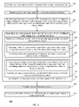
- FIG. 3 schematically shows an example of an embodiment of method 400 .
- Method 400 for recovering from a low-power period starts by stage 410 of maintaining a power gated circuit in a low power mode, during a low power period.
- Stage 410 is followed by stage 420 of receiving, by a control signal generator, a low power period end indicator.
- Stage 420 is followed by stage 430 of determining an intensity of a control current, charging the switch device gate, in response to a value of a continuous supply voltage at a port of the control signal generator, a value of the gated supply voltage and an output signal of high switching point buffer 160 that is inputted by the gated supply voltage.
- Stage 430 is followed by stage 440 of controlling the intensity of the control current in response to the determination.
- Stage 440 is followed by stage 450 of providing the control signal to a switch.
- Stage 450 is followed by stage 460 of providing, by the switch, in response to the control signal a gated supply voltage to a power gated circuit.
- Stage 440 can include stage 442 of generating, by a strong current drain, the draining current which is indifferent to the voltage drop during the first period.
- Stage 440 can also include stage 444 of generating, by the strong current drain, a week voltage drop responsive draining current during a second period.
- the voltage drop responsive draining current is responsive to a value of a voltage drop that represents a difference between the value of the continuous supply voltage at the port of the control signal generator and the value of the continuous supply voltage at a continuous voltage supply port.
- control current can include at least one of the voltage drop indifferent draining current and the voltage drop responsive draining current.
- Stage 440 can include stages 446 and 448 .
- Stage 446 includes controlling the strong current drain by a first branch of a strong current drain controller during the first period.
- Stage 448 includes controlling the strong current drain by a second branch of the strong current drain controller during the second period.
- Stage 448 can include stage 449 of translating, by a voltage adjustment element of the second branch, a low amount of voltage drop to a control voltage that activates the strong current drain and translating a high amount of retention power supply to a control voltage that deactivates the strong current drain.
- Stage 449 can include utilizing a voltage adjustment element that may include (but not necessarily) a forward biased diode.
- Stage 449 can include providing, by the second branch and to the gate of the strong current drain control, voltages within a voltage range that comprises the threshold voltage of the strong current drain.
- Stage 446 can include stage 447 of providing, by the first branch and to a gate of the strong current drain, control voltages that are much above a threshold voltage of the strong current drain.
- FIG. 4 schematically shows an example of an embodiment of method 500 .
- Method 500 for recovering from a low-power period starts by stage 410 of maintaining a power gated circuit in a low power mode, during a low power period.
- Stage 410 is followed by stage 420 of receiving, by a control signal generator, a low power period end indicator.
- Stage 420 is followed by stages 520 and 530 .
- Stage 520 includes determining an intensity of a voltage drop indifferent draining current generated by a strong current drain.
- Stage 520 is followed by stage 525 of generating, by a strong current drain, a voltage drop indifferent draining current during a first period.
- the first period starts after a reception of the low power end indicator and ends when the gated power supply voltage reaches a first value.
- Stage 530 includes determining an intensity of a voltage drop responsive draining current generated by a strong current drain.
- Stage 530 is followed by stage 535 of generating, by the strong current drain, a voltage drop responsive draining current during a second period.
- the second period starts after a beginning of the first period and ends when the gated supply voltage reaches a second value that is higher than the first value and causes the high switching point buffer to output a high value signal.
- the voltage drop responsive draining current is responsive to a value of a voltage drop that represents a difference between the value of the continuous power supply voltage at the port of the control signal generator and the value of the continuous supply voltage at a continuous voltage supply port.
- Stage 525 and 535 are followed by stage 540 of providing a control signal to a switch.
- the control signal includes at least one of the voltage drop indifferent draining current and the voltage drop responsive draining current.
- Stage 540 is followed by stage 550 of providing, by the switch, in response to the control signal, a gated supply current to a power gated circuit.
- Stage 525 can include controlling the strong current drain by a first branch of a strong current drain controller during the first period.
- Stage 535 can include controlling the strong current drain by a second branch of the strong current drain controller during the second period.
- Stage 535 can include mirroring by a voltage adjustment element that comprises a forward biased diode, the retention power supply voltage to the strong current drain control voltage.
- Stage 525 can include providing, by the first branch and to a gate of the strong current drain, control voltages that are much above a threshold voltage of the strong current drain; and stage 535 can include providing, by the second branch and to the gate of the strong current drain control, voltages within a voltage range that comprises the threshold voltage of the strong current drain.
- Either one of methods 400 and 500 can be implemented by system 200 of FIG. 1 .
- the power supply gating covers also the ground gating which is completely symmetric to the power supply gating.
- the elements of the system 200 change their polarity (e.g. NMOS transistor becomes PMOS transistor and vice-versa).
- current drains become current sources (and vice-versa), and the control signal polarity is also changing.
- any two components herein combined to achieve a particular functionality can be seen as “associated with” each other such that the desired functionality is achieved, irrespective of architectures or intermedial components.
- any two components so associated can also be viewed as being “operably connected,” or “operably coupled,” to each other to achieve the desired functionality.
Landscapes
- Engineering & Computer Science (AREA)
- Physics & Mathematics (AREA)
- Computer Hardware Design (AREA)
- Computing Systems (AREA)
- General Engineering & Computer Science (AREA)
- Mathematical Physics (AREA)
- Power Engineering (AREA)
- Electronic Switches (AREA)
Abstract
Description
Vddc=IRdrop+Vddcad (1)
-
- Especially,
diode 155 acts as a biasing element that convertsVddcad 185 toCV 182, wherein during thesecond period CV 182 can change (in response to changes in IRdrop) within a voltage range that includes the threshold voltage (Vth) offirst NMOS transistor 131. Thus, different values of IRdrop can activate or deactivate strongcurrent drain 130 and thus affect the value ofCC 181. In other words, forwardbiased diode 155 translates Vddcad 185 (actually responsive to the amount of IRdrop) to a voltage (CV 182) that activates strongcurrent drain 150 and translates a large amount of IRdrop to a control voltage decrease that deactivates the strong current drain.
- Especially,
Claims (20)
Priority Applications (2)
| Application Number | Priority Date | Filing Date | Title |
|---|---|---|---|
| US12/261,599 US8089259B2 (en) | 2008-10-30 | 2008-10-30 | Integrated circuit and a method for recovering from a low-power period |
| PCT/US2009/058130 WO2010096100A1 (en) | 2008-10-30 | 2009-09-24 | Integrated circuit and a method for recovering from a low-power period |
Applications Claiming Priority (1)
| Application Number | Priority Date | Filing Date | Title |
|---|---|---|---|
| US12/261,599 US8089259B2 (en) | 2008-10-30 | 2008-10-30 | Integrated circuit and a method for recovering from a low-power period |
Publications (2)
| Publication Number | Publication Date |
|---|---|
| US20100109633A1 US20100109633A1 (en) | 2010-05-06 |
| US8089259B2 true US8089259B2 (en) | 2012-01-03 |
Family
ID=42130592
Family Applications (1)
| Application Number | Title | Priority Date | Filing Date |
|---|---|---|---|
| US12/261,599 Active 2029-11-25 US8089259B2 (en) | 2008-10-30 | 2008-10-30 | Integrated circuit and a method for recovering from a low-power period |
Country Status (2)
| Country | Link |
|---|---|
| US (1) | US8089259B2 (en) |
| WO (1) | WO2010096100A1 (en) |
Cited By (1)
| Publication number | Priority date | Publication date | Assignee | Title |
|---|---|---|---|---|
| US9917581B2 (en) | 2012-05-29 | 2018-03-13 | Nxp Usa, Inc. | Electronic device and method for operating a power switch |
Families Citing this family (4)
| Publication number | Priority date | Publication date | Assignee | Title |
|---|---|---|---|---|
| US8228080B2 (en) * | 2009-07-24 | 2012-07-24 | Freescale Semiconductor, Inc. | Device and method for current estimation |
| US8542054B2 (en) * | 2011-10-31 | 2013-09-24 | Apple Inc. | Power switch acceleration scheme for fast wakeup |
| US9335809B2 (en) * | 2013-03-15 | 2016-05-10 | Seagate Technology Llc | Volatile memory storing system data during low power mode operation and monitoring the voltage supplied to the memory during low power mode |
| US9411394B2 (en) * | 2013-03-15 | 2016-08-09 | Seagate Technology Llc | PHY based wake up from low power mode operation |
Citations (12)
| Publication number | Priority date | Publication date | Assignee | Title |
|---|---|---|---|---|
| US5019770A (en) | 1988-10-26 | 1991-05-28 | Kyushu University | Switching power source device having energy recovery |
| US5534675A (en) | 1988-11-01 | 1996-07-09 | Sodick Co., Ltd. | Power supply system for electric discharge machines |
| US5736842A (en) | 1996-07-11 | 1998-04-07 | Delta Electronics, Inc. | Technique for reducing rectifier reverse-recovery-related losses in high-voltage high power converters |
| US6061253A (en) | 1997-12-03 | 2000-05-09 | Fuji Electrical Co., Ltd. | Variable frequency soft switching power supply with reduced noise and improved power factor |
| US6118261A (en) | 1993-11-08 | 2000-09-12 | International Business Machines Corp. | Slew rate control circuit |
| US6208194B1 (en) | 1998-12-31 | 2001-03-27 | Honeywell International Inc. | Synchronous rectifier MOFSET with controlled channel voltage drop |
| US20020047742A1 (en) | 2000-09-08 | 2002-04-25 | Mitsubishi Denki Kabushiki Kaisha | Semiconductor storage device with suppressed power consumption and reduced recovery time from suspend mode |
| US20020057076A1 (en) * | 2000-02-11 | 2002-05-16 | Champion Microelectronic Corp. | Low power mode and feedback arrangement for a switching power converter |
| US20030062947A1 (en) | 2001-10-01 | 2003-04-03 | International Rectifier Corporation | Power control circuit with active impedance to avoid interference and sensing problems |
| US20060033551A1 (en) | 2004-08-16 | 2006-02-16 | Wei Dong | Switch driver with slew rate control |
| US20070257705A1 (en) | 2006-02-03 | 2007-11-08 | Stmicroelectronics S.A. | Device for managing the consumption peak of a domain on each powering-up |
| US20090009151A1 (en) * | 2007-07-04 | 2009-01-08 | Texas Instruments Deutschland Gmbh | Reference voltage generator with bootstrapping effect |
-
2008
- 2008-10-30 US US12/261,599 patent/US8089259B2/en active Active
-
2009
- 2009-09-24 WO PCT/US2009/058130 patent/WO2010096100A1/en not_active Ceased
Patent Citations (12)
| Publication number | Priority date | Publication date | Assignee | Title |
|---|---|---|---|---|
| US5019770A (en) | 1988-10-26 | 1991-05-28 | Kyushu University | Switching power source device having energy recovery |
| US5534675A (en) | 1988-11-01 | 1996-07-09 | Sodick Co., Ltd. | Power supply system for electric discharge machines |
| US6118261A (en) | 1993-11-08 | 2000-09-12 | International Business Machines Corp. | Slew rate control circuit |
| US5736842A (en) | 1996-07-11 | 1998-04-07 | Delta Electronics, Inc. | Technique for reducing rectifier reverse-recovery-related losses in high-voltage high power converters |
| US6061253A (en) | 1997-12-03 | 2000-05-09 | Fuji Electrical Co., Ltd. | Variable frequency soft switching power supply with reduced noise and improved power factor |
| US6208194B1 (en) | 1998-12-31 | 2001-03-27 | Honeywell International Inc. | Synchronous rectifier MOFSET with controlled channel voltage drop |
| US20020057076A1 (en) * | 2000-02-11 | 2002-05-16 | Champion Microelectronic Corp. | Low power mode and feedback arrangement for a switching power converter |
| US20020047742A1 (en) | 2000-09-08 | 2002-04-25 | Mitsubishi Denki Kabushiki Kaisha | Semiconductor storage device with suppressed power consumption and reduced recovery time from suspend mode |
| US20030062947A1 (en) | 2001-10-01 | 2003-04-03 | International Rectifier Corporation | Power control circuit with active impedance to avoid interference and sensing problems |
| US20060033551A1 (en) | 2004-08-16 | 2006-02-16 | Wei Dong | Switch driver with slew rate control |
| US20070257705A1 (en) | 2006-02-03 | 2007-11-08 | Stmicroelectronics S.A. | Device for managing the consumption peak of a domain on each powering-up |
| US20090009151A1 (en) * | 2007-07-04 | 2009-01-08 | Texas Instruments Deutschland Gmbh | Reference voltage generator with bootstrapping effect |
Non-Patent Citations (1)
| Title |
|---|
| PCT/US2009/058130 Search Report and Written Opinion, Mailed May 3, 2010. |
Cited By (1)
| Publication number | Priority date | Publication date | Assignee | Title |
|---|---|---|---|---|
| US9917581B2 (en) | 2012-05-29 | 2018-03-13 | Nxp Usa, Inc. | Electronic device and method for operating a power switch |
Also Published As
| Publication number | Publication date |
|---|---|
| WO2010096100A1 (en) | 2010-08-26 |
| US20100109633A1 (en) | 2010-05-06 |
Similar Documents
| Publication | Publication Date | Title |
|---|---|---|
| US5828262A (en) | Ultra low power pumped n-channel output buffer with self-bootstrap | |
| US9473127B1 (en) | Input/output (I/O) driver | |
| US8089259B2 (en) | Integrated circuit and a method for recovering from a low-power period | |
| US6664805B2 (en) | Switched capacitor piecewise linear slew rate control methods for output devices | |
| US6720794B2 (en) | Output buffer circuit | |
| US9813051B2 (en) | Driving circuit for power switch | |
| US9536593B1 (en) | Low power receiver with wide input voltage range | |
| US8405424B2 (en) | Output buffer with adjustable feedback | |
| US8593205B2 (en) | Output buffer circuit and input/output buffer circuit | |
| US6833749B2 (en) | System and method for obtaining hysteresis through body substrate control | |
| US7355447B2 (en) | Level shifter circuit | |
| US20170012625A1 (en) | Voltage level shifter | |
| US20120286853A1 (en) | Semiconductor integrated circuit | |
| US6650152B2 (en) | Intermediate voltage control circuit having reduced power consumption | |
| KR100568107B1 (en) | High speed and low power voltage level conversion circuit | |
| US20040032287A1 (en) | Driver circuit | |
| US9112486B2 (en) | Asymmetric propagation delays in level shifters and related circuits | |
| US20240333281A1 (en) | Failsafe node voltage setting circuit | |
| US6426653B1 (en) | MOS output driver, and circuit and method of controlling same | |
| US9859888B2 (en) | Transmitter with feedback terminated preemphasis | |
| KR940003399B1 (en) | Output buffer for low noise of data | |
| US20260058655A1 (en) | Switch circuit control | |
| US11063587B1 (en) | Voltage on-off detector and electronic device including the same | |
| KR100432482B1 (en) | A fast swing-limited pullup circuit | |
| US6842051B1 (en) | Voltage detector circuit with application to variable voltage filter and variable output buffer |
Legal Events
| Date | Code | Title | Description |
|---|---|---|---|
| AS | Assignment |
Owner name: FREESCALE SEMICONDUCTOR, INC.,TEXAS Free format text: ASSIGNMENT OF ASSIGNORS INTEREST;ASSIGNORS:SOFER, SERGEY;GOLDMAN, VLAD;TZYTKIN, DOV;SIGNING DATES FROM 20080923 TO 20080925;REEL/FRAME:021764/0481 Owner name: FREESCALE SEMICONDUCTOR, INC., TEXAS Free format text: ASSIGNMENT OF ASSIGNORS INTEREST;ASSIGNORS:SOFER, SERGEY;GOLDMAN, VLAD;TZYTKIN, DOV;SIGNING DATES FROM 20080923 TO 20080925;REEL/FRAME:021764/0481 |
|
| AS | Assignment |
Owner name: CITIBANK, N.A.,NEW YORK Free format text: SECURITY AGREEMENT;ASSIGNOR:FREESCALE SEMICONDUCTOR, INC.;REEL/FRAME:022380/0409 Effective date: 20090216 Owner name: CITIBANK, N.A., NEW YORK Free format text: SECURITY AGREEMENT;ASSIGNOR:FREESCALE SEMICONDUCTOR, INC.;REEL/FRAME:022380/0409 Effective date: 20090216 |
|
| FEPP | Fee payment procedure |
Free format text: PAYOR NUMBER ASSIGNED (ORIGINAL EVENT CODE: ASPN); ENTITY STATUS OF PATENT OWNER: LARGE ENTITY |
|
| STCF | Information on status: patent grant |
Free format text: PATENTED CASE |
|
| AS | Assignment |
Owner name: CITIBANK, N.A., AS NOTES COLLATERAL AGENT, NEW YORK Free format text: SECURITY AGREEMENT;ASSIGNOR:FREESCALE SEMICONDUCTOR, INC.;REEL/FRAME:030633/0424 Effective date: 20130521 Owner name: CITIBANK, N.A., AS NOTES COLLATERAL AGENT, NEW YOR Free format text: SECURITY AGREEMENT;ASSIGNOR:FREESCALE SEMICONDUCTOR, INC.;REEL/FRAME:030633/0424 Effective date: 20130521 |
|
| AS | Assignment |
Owner name: CITIBANK, N.A., AS NOTES COLLATERAL AGENT, NEW YORK Free format text: SECURITY AGREEMENT;ASSIGNOR:FREESCALE SEMICONDUCTOR, INC.;REEL/FRAME:031591/0266 Effective date: 20131101 Owner name: CITIBANK, N.A., AS NOTES COLLATERAL AGENT, NEW YOR Free format text: SECURITY AGREEMENT;ASSIGNOR:FREESCALE SEMICONDUCTOR, INC.;REEL/FRAME:031591/0266 Effective date: 20131101 |
|
| FPAY | Fee payment |
Year of fee payment: 4 |
|
| AS | Assignment |
Owner name: FREESCALE SEMICONDUCTOR, INC., TEXAS Free format text: PATENT RELEASE;ASSIGNOR:CITIBANK, N.A., AS COLLATERAL AGENT;REEL/FRAME:037354/0807 Effective date: 20151207 |
|
| AS | Assignment |
Owner name: MORGAN STANLEY SENIOR FUNDING, INC., MARYLAND Free format text: ASSIGNMENT AND ASSUMPTION OF SECURITY INTEREST IN PATENTS;ASSIGNOR:CITIBANK, N.A.;REEL/FRAME:037486/0517 Effective date: 20151207 |
|
| AS | Assignment |
Owner name: MORGAN STANLEY SENIOR FUNDING, INC., MARYLAND Free format text: ASSIGNMENT AND ASSUMPTION OF SECURITY INTEREST IN PATENTS;ASSIGNOR:CITIBANK, N.A.;REEL/FRAME:037518/0292 Effective date: 20151207 |
|
| AS | Assignment |
Owner name: MORGAN STANLEY SENIOR FUNDING, INC., MARYLAND Free format text: SUPPLEMENT TO THE SECURITY AGREEMENT;ASSIGNOR:FREESCALE SEMICONDUCTOR, INC.;REEL/FRAME:039138/0001 Effective date: 20160525 |
|
| AS | Assignment |
Owner name: NXP, B.V., F/K/A FREESCALE SEMICONDUCTOR, INC., NETHERLANDS Free format text: RELEASE BY SECURED PARTY;ASSIGNOR:MORGAN STANLEY SENIOR FUNDING, INC.;REEL/FRAME:040925/0001 Effective date: 20160912 Owner name: NXP, B.V., F/K/A FREESCALE SEMICONDUCTOR, INC., NE Free format text: RELEASE BY SECURED PARTY;ASSIGNOR:MORGAN STANLEY SENIOR FUNDING, INC.;REEL/FRAME:040925/0001 Effective date: 20160912 |
|
| AS | Assignment |
Owner name: NXP B.V., NETHERLANDS Free format text: RELEASE BY SECURED PARTY;ASSIGNOR:MORGAN STANLEY SENIOR FUNDING, INC.;REEL/FRAME:040928/0001 Effective date: 20160622 |
|
| AS | Assignment |
Owner name: NXP USA, INC., TEXAS Free format text: CHANGE OF NAME;ASSIGNOR:FREESCALE SEMICONDUCTOR, INC.;REEL/FRAME:040632/0001 Effective date: 20161107 |
|
| AS | Assignment |
Owner name: MORGAN STANLEY SENIOR FUNDING, INC., MARYLAND Free format text: CORRECTIVE ASSIGNMENT TO CORRECT THE REMOVE PATENTS 8108266 AND 8062324 AND REPLACE THEM WITH 6108266 AND 8060324 PREVIOUSLY RECORDED ON REEL 037518 FRAME 0292. ASSIGNOR(S) HEREBY CONFIRMS THE ASSIGNMENT AND ASSUMPTION OF SECURITY INTEREST IN PATENTS;ASSIGNOR:CITIBANK, N.A.;REEL/FRAME:041703/0536 Effective date: 20151207 |
|
| AS | Assignment |
Owner name: NXP USA, INC., TEXAS Free format text: CORRECTIVE ASSIGNMENT TO CORRECT THE NATURE OF CONVEYANCE PREVIOUSLY RECORDED AT REEL: 040632 FRAME: 0001. ASSIGNOR(S) HEREBY CONFIRMS THE MERGER AND CHANGE OF NAME;ASSIGNOR:FREESCALE SEMICONDUCTOR INC.;REEL/FRAME:044209/0047 Effective date: 20161107 |
|
| AS | Assignment |
Owner name: SHENZHEN XINGUODU TECHNOLOGY CO., LTD., CHINA Free format text: CORRECTIVE ASSIGNMENT TO CORRECT THE TO CORRECT THE APPLICATION NO. FROM 13,883,290 TO 13,833,290 PREVIOUSLY RECORDED ON REEL 041703 FRAME 0536. ASSIGNOR(S) HEREBY CONFIRMS THE THE ASSIGNMENT AND ASSUMPTION OF SECURITYINTEREST IN PATENTS.;ASSIGNOR:MORGAN STANLEY SENIOR FUNDING, INC.;REEL/FRAME:048734/0001 Effective date: 20190217 Owner name: SHENZHEN XINGUODU TECHNOLOGY CO., LTD., CHINA Free format text: CORRECTIVE ASSIGNMENT TO CORRECT THE TO CORRECT THE APPLICATION NO. FROM 13,883,290 TO 13,833,290 PREVIOUSLY RECORDED ON REEL 041703 FRAME 0536. ASSIGNOR(S) HEREBY CONFIRMS THE THE ASSIGNMENT AND ASSUMPTION OF SECURITY INTEREST IN PATENTS.;ASSIGNOR:MORGAN STANLEY SENIOR FUNDING, INC.;REEL/FRAME:048734/0001 Effective date: 20190217 |
|
| MAFP | Maintenance fee payment |
Free format text: PAYMENT OF MAINTENANCE FEE, 8TH YEAR, LARGE ENTITY (ORIGINAL EVENT CODE: M1552); ENTITY STATUS OF PATENT OWNER: LARGE ENTITY Year of fee payment: 8 |
|
| AS | Assignment |
Owner name: NXP B.V., NETHERLANDS Free format text: RELEASE BY SECURED PARTY;ASSIGNOR:MORGAN STANLEY SENIOR FUNDING, INC.;REEL/FRAME:050744/0097 Effective date: 20190903 |
|
| AS | Assignment |
Owner name: MORGAN STANLEY SENIOR FUNDING, INC., MARYLAND Free format text: CORRECTIVE ASSIGNMENT TO CORRECT THE REMOVE APPLICATION11759915 AND REPLACE IT WITH APPLICATION 11759935 PREVIOUSLY RECORDED ON REEL 037486 FRAME 0517. ASSIGNOR(S) HEREBY CONFIRMS THE ASSIGNMENT AND ASSUMPTION OF SECURITYINTEREST IN PATENTS;ASSIGNOR:CITIBANK, N.A.;REEL/FRAME:053547/0421 Effective date: 20151207 Owner name: MORGAN STANLEY SENIOR FUNDING, INC., MARYLAND Free format text: CORRECTIVE ASSIGNMENT TO CORRECT THE REMOVE APPLICATION 11759915 AND REPLACE IT WITH APPLICATION 11759935 PREVIOUSLY RECORDED ON REEL 037486 FRAME 0517. ASSIGNOR(S) HEREBY CONFIRMS THE ASSIGNMENT AND ASSUMPTION OF SECURITY INTEREST IN PATENTS;ASSIGNOR:CITIBANK, N.A.;REEL/FRAME:053547/0421 Effective date: 20151207 |
|
| AS | Assignment |
Owner name: NXP B.V., NETHERLANDS Free format text: CORRECTIVE ASSIGNMENT TO CORRECT THE REMOVEAPPLICATION 11759915 AND REPLACE IT WITH APPLICATION11759935 PREVIOUSLY RECORDED ON REEL 040928 FRAME 0001. ASSIGNOR(S) HEREBY CONFIRMS THE RELEASE OF SECURITYINTEREST;ASSIGNOR:MORGAN STANLEY SENIOR FUNDING, INC.;REEL/FRAME:052915/0001 Effective date: 20160622 Owner name: NXP B.V., NETHERLANDS Free format text: CORRECTIVE ASSIGNMENT TO CORRECT THE REMOVE APPLICATION 11759915 AND REPLACE IT WITH APPLICATION 11759935 PREVIOUSLY RECORDED ON REEL 040928 FRAME 0001. ASSIGNOR(S) HEREBY CONFIRMS THE RELEASE OF SECURITY INTEREST;ASSIGNOR:MORGAN STANLEY SENIOR FUNDING, INC.;REEL/FRAME:052915/0001 Effective date: 20160622 |
|
| AS | Assignment |
Owner name: NXP, B.V. F/K/A FREESCALE SEMICONDUCTOR, INC., NETHERLANDS Free format text: CORRECTIVE ASSIGNMENT TO CORRECT THE REMOVEAPPLICATION 11759915 AND REPLACE IT WITH APPLICATION11759935 PREVIOUSLY RECORDED ON REEL 040925 FRAME 0001. ASSIGNOR(S) HEREBY CONFIRMS THE RELEASE OF SECURITYINTEREST;ASSIGNOR:MORGAN STANLEY SENIOR FUNDING, INC.;REEL/FRAME:052917/0001 Effective date: 20160912 Owner name: NXP, B.V. F/K/A FREESCALE SEMICONDUCTOR, INC., NETHERLANDS Free format text: CORRECTIVE ASSIGNMENT TO CORRECT THE REMOVE APPLICATION 11759915 AND REPLACE IT WITH APPLICATION 11759935 PREVIOUSLY RECORDED ON REEL 040925 FRAME 0001. ASSIGNOR(S) HEREBY CONFIRMS THE RELEASE OF SECURITY INTEREST;ASSIGNOR:MORGAN STANLEY SENIOR FUNDING, INC.;REEL/FRAME:052917/0001 Effective date: 20160912 |
|
| MAFP | Maintenance fee payment |
Free format text: PAYMENT OF MAINTENANCE FEE, 12TH YEAR, LARGE ENTITY (ORIGINAL EVENT CODE: M1553); ENTITY STATUS OF PATENT OWNER: LARGE ENTITY Year of fee payment: 12 |