CROSS-REFERENCE TO RELATED APPLICATIONS
This application is based upon and claims the benefit of priority from the prior Japanese Patent Application No. 2008-208691, filed on Aug. 13, 2008; the entire contents of which are incorporated herein by reference.
BACKGROUND
A micro electro mechanical system (MEMS) is configured by having mechanical parts, a sensor, an actuator, and an electronic circuit integrated together on the same substrate. The MEMS is used for various devices such as a printer head and a pressure sensor.
When the MEMS is used as a high-frequency device such as an impedance matching circuit and a high-frequency switch, losses can be suppressed.
Meanwhile, at the time of integrating mechanical parts and the like together on the same substrate, these mechanical parts can be easily integrated with electronic parts while using the same semiconductor manufacturing process. Therefore, a silicon substrate is used in many cases. When a cavity structure is formed on the silicon substrate, a movable unit is manufactured above the silicon substrate, and by performing an operation while using oscillation or deflection of the movable unit, characteristics of the MEMS can be obtained.
In the MEMS, to prevent the cavity structure formed on the silicon substrate from being crushed in a molding process and the like, the cavity structure is protected by a protection cap arranged above the silicon substrate. This protection cap is required with a gap between a pad formed on the silicon substrate and the protection cap to make it possible to connect the pad by wire bonding.
For example, Japanese Patent Application Laid-open No. 2007-222956 discloses the following method. A wiring layer is formed to surround a MEMS structure, and a silicon nitride film continuous from above the wiring layer to above the MEMS structure is formed. Plural openings are then formed on the silicon nitride film, and a cavity is formed between the semiconductor substrate and the silicon nitride film. The openings of the silicon nitride film are then closed, thereby air-tightly sealing the inside of the cavity.
However, when a MEMS is formed on a silicon substrate, a parasitic capacitance is generated between a wiring layer formed on the silicon substrate and the silicon substrate. Therefore, there is a problem that a high-frequency characteristic is degraded.
When a cavity structure is formed in the entire wiring region to reduce the parasitic capacitance between the wiring layer and the silicon substrate, the cavity structure is deviated from the protection cap, and this portion is crushed in a molding process and the like. Consequently, according to the conventional MEMS, a cavity structure cannot be provided at the outside of the protection cap. At the outside of the protection cap, a parasitic capacitance between the wiring layer and the silicon substrate cannot be reduced.
BRIEF SUMMARY OF THE INVENTION
A micro movable device according to an embodiment of the present invention comprises: a movable unit formed above a semiconductor substrate; a protection cap that is arranged above the semiconductor substrate and the movable unit and protects the movable unit; a signal line that are formed above the semiconductor substrate and transmit a high-frequency signal, a part of the signal line being provided below the movable unit; and an insulation layer that has a projection formed to project upward from the semiconductor substrate, the projection being provided at outside of the movable unit in a plain view and the insulation layer having a coated surface with the signal line, the coated surface being provided in a higher position than a bottom of the signal line below the movable unit.
A micro movable device according to an embodiment of the present invention comprises: a movable unit formed above a semiconductor substrate; a first insulation layer formed above the semiconductor substrate below the movable unit with a gap between the movable unit and the first insulation layer; a protection cap that is arranged above the first insulation layer and the movable unit and protects the movable unit; a first signal line that is arranged at inside of the protection cap and is formed on the first insulation layer with a gap between the movable unit and the first signal line and a part of the first signal being provided below the movable unit and the first insulation layer; a second insulation layer that are arranged at outside of the protection cap and has a projection formed to project upward from the first insulation layer; and a second signal line electrically connected to the first signal line, and coating a surface of the projection of the second insulation layer, the second signal line being provided in a higher position than the part of the first signal line.
A micro movable device according to an embodiment of the present invention comprises: a movable unit formed above a semiconductor substrate; a first insulation layer formed above the semiconductor substrate below the movable unit with a gap between the movable unit and the insulation layer; a protection cap that is arranged above the first insulation layer and the movable unit and protects the movable unit; a first signal line that is arranged at inside of the protection cap and is formed on the first insulation layer with a gap between the movable unit and the first signal line; a second insulation layer that is arranged at outside of the protection cap and has a projection formed to project upward from the first insulation layer; a second signal line electrically connected to the first signal line, and coating a surface of the projection of the second insulation layer; a first ground line that is arranged at inside of the protection cap and is formed on the first insulation layer; a third insulation layer that is arranged at outside of the protection cap and has a projection formed to project upward from the first insulation layer; and a second ground line electrically connected to the first ground line and coating an entire exposed surface of the third insulation layer.
BRIEF DESCRIPTION OF THE DRAWINGS
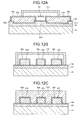
FIG. 1 is a plan view of a schematic configuration of a micro movable device according to a first embodiment of the present invention;
FIG. 2A is a cross-sectional view cut along a line A1-A1′ in FIG. 1;
FIG. 2B is a cross-sectional view cut along a line C1-C1′ in FIG. 1;
FIG. 2C is a cross-sectional view cut along a line B1-B1′ in FIG. 1;
FIGS. 3A to 3C are cross-sectional views of a method of manufacturing the micro movable device shown in FIG. 1;
FIGS. 4A and 4B are cross-sectional views of the method of manufacturing the micro movable device shown in FIG. 1;
FIG. 5 is a plan view of a schematic configuration of a micro movable device according to a second embodiment of the present invention;
FIG. 6A is a cross-sectional view cut along a line A2-A2′ in FIG. 5;
FIG. 6B is a cross-sectional view cut along a line B2-B2′ in FIG. 5;
FIG. 7 is a plan view of a schematic configuration of a micro movable device according to a third embodiment of the present invention;
FIG. 8A is a cross-sectional view cut along a line A3-A3′ in FIG. 7;
FIG. 8B is a cross-sectional view cut along a line B3-B3′ in FIG. 7;
FIG. 9 is a plan view of a schematic configuration of a micro movable device according to a fourth embodiment of the present invention;
FIG. 10A is a cross-sectional view cut along a line A4-A4′ in FIG. 9;
FIG. 10B is a cross-sectional view cut along a line B4-B4′ in FIG. 9;
FIG. 11 is a plan view of a schematic configuration of a micro movable device according to a fifth embodiment of the present invention;
FIG. 12A is a cross-sectional view cut along a line A5-A5′ in FIG. 11;
FIG. 12B is a cross-sectional view cut along a line B5-B5′ in FIG. 11;
FIG. 12C is a cross-sectional view cut along a line C5-C5′ in FIG. 11; and
FIG. 13 is a cross-sectional view of a value of a parasitic capacitance between a semiconductor substrate and a wiring layer according to the third embodiment in comparison with a parasitic capacitance value according to a conventional example.
DETAILED DESCRIPTION OF THE INVENTION
Exemplary embodiments of a micro movable device according to the present invention will be explained below in detail with reference to the accompanying drawings. The present invention is not limited thereto.
FIG. 1 is a plan view of a schematic configuration of a micro movable device according to a first embodiment of the present invention. FIG. 2A is a cross-sectional view cut along a line A1-A1′ in FIG. 1. FIG. 2B is a cross-sectional view cut along a line C1-C1′ in FIG. 1. FIG. 2C is a cross-sectional view cut along a line B1-B1′ in FIG. 1.
In FIG. 1 and FIGS. 2A to 2C, an insulation layer 12 is formed on a semiconductor substrate 11. Ground lines 13 and 14 are arranged in parallel with each other on the insulation layer 12. Signal lines 15 a to 15 c physically isolated from each other are arranged between the ground lines 13 and 14. An insulation layer 16 is formed on the ground lines 13 and 14 and on the signal lines 15 a to 15 c. Pads P1 are formed by exposing ends of the ground lines 13 and 14 and the signal lines 15 a and 15 c, respectively from the insulation layer 16.
A movable line 19 is formed to stride the signal line 15 b above the semiconductor substrate 11, and both ends of the movable line 19 are connected to the ground lines 13 and 14, respectively via contacts C1. The movable line 19 is supported above the semiconductor substrate 11 to have a gap between the movable line 19 and the signal line 15 b, and a cavity is formed between the movable line 19 and the signal line 15 b.
A protection cap 20 for protecting the movable line 19 from external pressure is arranged above the semiconductor substrate 11 to have a gap between the pads P1 and the protection cap 20.
At the outside of the protection cap 20, a thick-film insulation layer 17 a arranged between the signal lines 15 a and 15 b is formed, and a thick-film insulation layer 17 b arranged between the signal lines 15 b and 15 c is formed, respectively. The thick-film insulation layers 17 a and 17 b can be formed above the semiconductor substrate 11 to project upward from the signal lines 15 a to 15 c. Signal lines 18 a and 18 b are formed to coat entire exposed surfaces of the thick-film insulation layers 17 a and 17 b, respectively. The signal line 18 a is connected to the signal lines 15 a and 15 b, and the signal line 18 b is connected to the signal lines 15 b and 15 c.
A material of the semiconductor substrate 11 is not limited to silicon, and can be Ge, SiGe, SiC, SiSn, PbS, GaAs, InP, GaP, GaN, ZnSe, GaInAsP, for example. For materials of the insulation layers 12 and 16, a silicon oxide film and a silicon nitride film can be used, for example. For materials of the ground lines 13 and 14, the signal lines 15 a to 15 c, and the movable line 19, metals such as Al and Cu can be used, for example. For materials of the thick-film insulation layers 17 a and 17 b, photosensitive polyimide or spin on glass (SOG) can be used, for example. A sacrifice film can be used to form a cavity between the movable line 19 and the signal line 15 b.
A position of the movable line 19 in a height direction and positions of the signal lines 18 a and 18 b in a height direction arranged on the thick-film insulation layers 17 a and 17 b, respectively can be set equal to each other.
A high-frequency signal Sr such as a radio frequency (RF) is input to the signal lines 15 a to 15 c and 18 a and 18 b, and a drive signal for driving the movable line 19 is input. When the signal lines 15 a to 15 c, and 18 a and 18 b become in a high potential based on the drive signal, the movable line 19 is pulled to the signal line 15 b, and the high-frequency signal Sr flows to the ground lines 13 and 14 based on a capacitance coupling between the movable line 19 and the signal line 15 b. On the other hand, when the signal lines 15 a to 15 c, and 18 a and 18 b become in a low potential based on the drive signal, a gap between the movable line 19 and the signal line 15 b becomes large, and the high-frequency signal Sr passes through the signal lines 15 a to 15 c, and 18 a and 18 b without flowing to the ground lines 13 and 14.
When the ground lines 13 and 14 and the signal lines 15 a to 15 c, 18 a and 18 b are formed on the semiconductor substrate 11, parasitic resistors 7 and 8 are formed between the ground lines 13 and 14 and the signal line 18 b, respectively, as shown in FIG. 2C, for example. Parasitic capacitors 1 to 4 are formed between the signal line 18 b and the semiconductor substrate 11, a parasitic capacitor 5 is formed between the ground line 13 and the semiconductor substrate 11, and a parasitic capacitor 6 is formed between the ground line 14 and the semiconductor substrate 11.
When the thick-film insulation layer 17 b is formed on the insulation layer 16, the parasitic capacitor 1 can be connected in series with the parasitic capacitor 2, and parasitic capacitance of the signal line 18 a can be reduced more than the reduction achieved when the signal line 18 a is directly formed on the insulation layer 12. Therefore, parasitic capacitance between the signal lines 18 a and 18 b and the semiconductor substrate 11 can be reduced without forming a cavity structure in the signal lines 18 a and 18 b at the outside of the protection cap 20. Consequently, a high-frequency characteristic can be improved while preventing the signal lines 18 a and 18 b from being crushed in the molding process and the like.
FIGS. 3A to 3C and FIGS. 4A and 4B are cross-sectional views of a method of manufacturing the micro movable device shown in FIG. 1.
In FIG. 3A, the insulation layer 12 is formed on the semiconductor substrate 11 by using a chemical vapor deposition (CVD) method or the like. A metal film is formed on the insulation layer 12 by using sputtering or vapor deposition. The metal film is patterned by using a photolithographic technique and an etching technique, thereby forming the ground lines 13 and 14 and the signal lines 15 a to 15 c shown in FIG. 1.
The insulation layer 16 is formed on the ground lines 13 and 14 and the signal lines 15 a to 15 c by using the CVD method and the like. The insulation layer 16 is patterned by using the photolithographic technique and the etching technique, thereby forming openings KO arranged at ends of the signal lines 15 a to 15 c on the insulation layer 16, and forming the pads P1.
As shown in FIG. 3B, a sacrifice film 17 made of photosensitive polyimide or SOG is formed on the insulation layer 16 by coating or the like. The sacrifice film 17 is patterned by using the photolithographic technique and the etching technique, thereby exposing the ends of the signal lines 15 a and 15 c via the openings K0, and forming on the sacrifice film 17 openings K1 that isolate the sacrifice film 17 in an island shape between the mutually isolated signal lines 15 a to 15 c.
Next, as shown in FIG. 3C, a metal film is formed on the sacrifice film 17 to fill the openings K0 and K1 by sputtering or deposition. The metal film is patterned by using the photolithographic technique and the etching technique, thereby forming the signal lines 18 a and 18 b and the movable line 19 on the sacrifice film 17.
As shown in FIG. 4A, the sacrifice film 17 is removed from the top of the semiconductor substrate 11 by using a wet etching method or the like, a cavity is formed between the movable line 19 and the signal line 15 b, and the thick-film insulation layers 17 a and 17 b of which entire exposed surfaces are coated by the signal lines 18 a and 18 b, respectively are formed on the insulation layer 16.
As shown in FIG. 4B, the protection cap 20 for protecting the movable line 19 from external pressure is formed above the semiconductor substrate 11 so that the signal lines 18 a and 18 b are arranged at the outside of the protection cap 20. Thereafter, a bonding wire is connected to the pads P1, and the semiconductor substrate 11 in its entirety is molded, thereby sealing a MEMS structure on the semiconductor substrate 11.
When the sacrifice film 17 is used for the thick-film insulation layers 17 a and 17 b and also when entire exposed surfaces of the thick-film insulation layers 17 a and 17 b are coated by the signal lines 18 a and 18 b, a separate provision of a process of forming the thick-film insulation layers 17 a and 17 b is not necessary. Further, at the time of removing the sacrifice film 17, removal of the thick-film insulation layers 17 a and 17 b can be prevented, thereby simplifying a manufacturing process.
FIG. 5 is a plan view of a schematic configuration of a micro movable device according to a second embodiment of the present invention. FIG. 6A is a cross-sectional view cut along a line A2-A2′ in FIG. 5. FIG. 6B is a cross-sectional view cut along a line B2-B2′ in FIG. 5.
In FIG. 5 and FIGS. 6A and 6B, an insulation layer 32 is formed on a semiconductor substrate 31. Ground lines 33 a to 33 c are arranged in a constant direction, and ground lines 34 a to 34 c are arranged in parallel with the ground lines 33 a to 33 c, on the insulation layer 32. Signal lines 35 a to 35 c are arranged between the ground lines 33 a to 33 c and the ground lines 34 a to 34 c. The ground lines 33 a to 33 c are isolated from each other, the ground lines 34 a to 34 c are isolated from each other, and the signal lines 35 a to 35 c are isolated from each other.
An insulation layer 36 is formed on the ground lines 33 a to 33 c, and 34 a to 34 c, and on the signal lines 35 a to 35 c. Pads P11 are formed by exposing one ends of the ground lines 33 a, 33 c, 34 a, and 34 c and the signal lines 35 a and 35 c, respectively from the insulation layer 36.
A movable line 39 is formed to stride the signal line 35 b above the semiconductor substrate 31, and both ends of the movable line 39 are connected to the ground lines 33 b and 34 b, respectively via contacts C11. The movable line 39 is supported above the semiconductor substrate 31 to have a gap between the movable line 39 and the signal line 35 b, and a cavity is formed between the movable line 39 and the signal line 35 b.
A protection cap 40 for protecting the movable line 39 from external pressure is arranged above the semiconductor substrate 31 to have a gap between the pads P11 and the protection cap 40.
At the outside of the protection cap 40, a thick-film insulation layer 37 a arranged between the signal lines 35 a and 35 b is formed, and a thick-film insulation layer 37 b arranged between the signal lines 35 b and 35 c is formed, respectively. At the outside of the protection cap 40, a thick-film insulation layer 37 c arranged between the ground lines 33 a and 33 b is formed, and a thick-film insulation layer 37 d arranged between the ground lines 33 b and 33 c is formed, respectively. Further, at the outside of the protection cap 40, a thick-film insulation layer 37 e arranged between the ground lines 34 a and 34 b is formed, and a thick-film insulation layer 37 f arranged between the ground lines 34 b and 34 c is formed, respectively.
The thick-film insulation layers 37 a to 37 f can be formed above the semiconductor substrate 31 to project upward from the ground lines 33 a to 33 c, and 34 a to 34 c, and from the signal lines 35 a to 35 c. Signal lines 38 a and 38 b are formed to coat entire exposed surfaces of the thick-film insulation layers 37 a and 37 b, respectively. The signal line 38 a is connected to the signal lines 35 a and 35 b, and the signal line 38 b is connected to the signal lines 35 b and 35 c. Ground lines 38 c and 38 d are formed to coat entire exposed surfaces of the thick-film insulation layers 37 c and 37 d, respectively. The ground line 38 c is connected to the ground lines 33 a and 33 b, and the ground line 38 d is connected to the ground lines 33 b and 33 c. Ground lines 38 e and 38 f are formed to coat entire exposed surfaces of the thick-film insulation layers 37 e and 37 f, respectively. The ground line 38 e is connected to the ground lines 34 a and 34 b, and the ground line 38 f is connected to the ground lines 34 b and 34 c.
With this arrangement, not only parasitic capacitances of the signal lines 38 a and 38 b can be reduced but also parasitic capacitances of the ground lines 38 c to 38 f can be reduced without forming cavity structures in the signal lines 35 a and 35 c and the ground lines 33 a, 33 c, 34 a, and 34 c at the outside of the protection cap 40. Therefore, a high-frequency characteristic can be further improved while preventing the signal lines 38 a and 38 b and the ground lines 38 c to 38 f from being crushed in the molding process and the like.
A position of the movable line 39 in a height direction and positions of the signal lines 38 a and 38 b and the ground lines 38 c to 38 f in a height direction arranged on the thick-film insulation layers 37 a to 37 f, respectively can be set equal to each other.
Consequently, the thick-film insulation layers 37 a to 37 f can be formed by using the sacrifice film 17 shown in FIGS. 2A to 2C. In forming the thick-film insulation layers 37 c to 37 f beneath the ground lines 38 c to 38 f, a separate provision of a process of forming the thick-film insulation layers 37 a to 37 f is not necessary. As a result, a manufacturing process can be simplified.
FIG. 7 is a plan view of a schematic configuration of a micro movable device according to a third embodiment of the present invention. FIG. 8A is a cross-sectional view cut along a line A3-A3′ in FIG. 7. FIG. 8B is a cross-sectional view cut along a line B3-B3′ in FIG. 7.
In FIG. 7 and FIGS. 8A and 8B, an insulation layer 52 is formed on a semiconductor substrate 51. On the insulation layer 52, ground lines 53 a to 53 e are arranged in a constant direction, ground lines 54 a to 54 e are arranged in parallel with the ground lines 53 a to 53 e, and signal lines 55 a to 55 e are arranged between the ground lines 53 a to 53 e and 54 a to 54 e. The ground lines 53 a to 53 e are isolated from each other, the ground lines 54 a to 54 e are isolated from each other, and the signal lines 55 a to 55 e are isolated from each other.
An insulation layer 56 is formed on the ground lines 53 a to 53 e, and 54 a to 54 e, and on the signal lines 55 a to 55 e. Pads P21 are formed by exposing one ends of the ground lines 53 a, 53 c, 54 a, and 54 c and the signal lines 55 a and 55 c, respectively from the insulation layer 56.
A movable line 59 is formed to stride the signal line 55 b above the semiconductor substrate 51, and both ends of the movable line 59 are connected to the ground lines 53 b and 54 b, respectively via contacts C21. The movable line 59 is supported above the semiconductor substrate 51 to have a gap between the movable line 59 and the signal line 55 b, and a cavity is formed between the movable line 59 and the signal line 55 b.
A protection cap 60 for protecting the movable line 59 from external pressure is arranged above the semiconductor substrate 51 to have a gap between the pads P21 and the protection cap 60.
At the outside of the protection cap 60, a thick-film insulation layer 57 a arranged between the signal lines 55 a and 55 b is formed, and a thick-film insulation layer 57 b arranged between the signal lines 55 b and 55 c is formed, respectively. At the outside of the protection cap 60, a thick-film insulation layer 57 c arranged between the ground lines 53 a and 53 b is formed, and a thick-film insulation layer 57 d arranged between the ground lines 53 b and 53 c is formed, respectively. Further, at the outside of the protection cap 60, a thick-film insulation layer 57 e arranged between the ground lines 54 a and 54 b is formed, and a thick-film insulation layer 57 f arranged between the ground lines 54 b and 54 c is formed, respectively.
The thick-film insulation layers 57 a to 57 f can be formed above the semiconductor substrate 51 to project upward from the ground lines 53 a to 53 c, and 54 a to 54 c, and from the signal lines 55 a to 55 c. Signal lines 58 a and 58 b are formed to coat entire exposed surfaces of the thick-film insulation layers 57 a and 57 b, respectively. The signal line 58 a is connected to the signal lines 55 a and 55 b, and the signal line 58 b is connected to the signal lines 55 b and 55 c. Ground lines 58 c and 58 d are formed to coat entire exposed surfaces of the thick-film insulation layers 57 c and 57 d, respectively. The ground line 58 c is connected to the ground lines 53 a and 53 b, and the ground line 58 d is connected to the ground lines 53 b and 53 c. Ground lines 58 e and 58 f are formed to coat entire exposed surfaces of the thick-film insulation layers 57 e and 57 f, respectively. The ground line 58 e is connected to the ground lines 54 a and 54 b, and the ground line 58 f is connected to the ground lines 54 b and 54 c.
At the inside of the protection cap 60, a signal line 58 g connecting between the signal lines 55 b and 55 d is formed, a signal line 58 h connecting between the signal lines 55 b and 55 e is formed, and a cavity is formed beneath the signal lines 58 g and 58 h. At the inside of the protection cap 60, a ground line 58 i connecting between the ground lines 53 b and 53 d is formed, a ground line 58 j connecting between the ground lines 53 b and 53 e is formed, and a cavity is formed beneath the ground lines 58 i and 58 j. Further, at the inside of the protection cap 60, a ground line 58 k connecting between the ground lines 54 b and 54 d is formed, a ground line 58 l connecting between the ground lines 54 b and 54 d is formed, and a cavity is formed beneath the ground lines 58 k and 58 l.
With this arrangement, not only parasitic capacitances of the signal lines 58 a and 58 b and the ground lines 58 c to 58 f can be reduced but also parasitic capacitances of the signal lines 58 g and 58 h and the ground lines 58 i to 58 l at the inside of the protection cap 60 can be reduced without forming cavity structures in the signal lines 55 a and 55 c and the ground lines 53 a, 53 c, 54 a, and 54 c at the outside of the protection cap 60. Therefore, a high-frequency characteristic can be further improved while preventing the signal lines 58 a and 58 b and the ground lines 58 c to 58 f from being crushed in the molding process and the like.
A position of the movable line 59 in a height direction, positions of the signal lines 58 a and 58 b and the ground lines 58 c to 58 f in a height direction arranged respectively on the thick-film insulation layers 57 a to 57 f, and positions of the signal lines 58 g and 58 h and the ground lines 58 i to 58 l arranged at the inside of the protection cap 60, respectively can be set equal to each other.
For a method of forming cavity structures beneath the signal lines 58 g and 58 h and the ground lines 58 i to 58 l, there can be used a method of forming the signal lines 58 g and 58 h and the ground lines 58 i to 58 l on the sacrifice film 17 shown in FIGS. 3A to 3C and FIGS. 4A to 4B, and then removing the sacrifice film 17 from beneath the signal lines 58 g and 58 h and the ground lines 58 i to 58 l. In removing the sacrifice film 17, to form the thick-film insulation layers 57 a to 57 f by leaving the sacrifice film 17 beneath the signal lines 58 a and 58 b and the ground lines 58 c to 58 f, the signal lines 58 a and 58 b and the ground lines 58 c to 58 f coat an entire exposed surface of the sacrifice film 17. To form cavity structures beneath the signal lines 58 g and 58 h and the ground lines 58 i to 58 l, the signal lines 58 g and 58 h and the ground lines 58 i to 58 l are not formed on sidewalls of the cavity film 17, without coating the entire exposed surface of the sacrifice film 17 by the signal lines 58 g and 58 h and the ground lines 58 i to 58 l.
In the third embodiment, there has been explained a method of forming the thick-film insulation layers 57 a to 57 f beneath the signal lines 58 a and 58 b and the ground lines 58 c to 58 f, and thereafter forming cavities beneath the signal lines 58 g and 58 h and the ground lines 58 i to 58 l. Alternatively, the thick-film insulation layers 57 a and 57 b can be formed only beneath the signal lines 58 a and 58 b, and at the same time, cavities can be formed only beneath the signal lines 58 g and 58 h.
FIG. 9 is a plan view of a schematic configuration of a micro movable device according to a fourth embodiment of the present invention. FIG. 10A is a cross-sectional view cut along a line A4-A4′ in FIG. 9. FIG. 10B is a cross-sectional view cut along a line B4-B4′ in FIG. 9.
In FIG. 9 and FIGS. 10A and 8B, an insulation layer 72 is formed on a semiconductor substrate 71. On the insulation layer 72, ground lines 73 a to 73 e are arranged in a constant direction, ground lines 74 a to 74 e are arranged in parallel with the ground lines 73 a to 73 e, and signal lines 75 a to 75 e are arranged between the ground lines 73 a to 73 e and 74 a to 74 e. The ground lines 73 a to 73 e are isolated from each other, the ground lines 74 a to 74 e are isolated from each other, and the signal lines 75 a to 75 e are isolated from each other. An insulation layer 76 is formed on the ground lines 73 a to 73 e, 74 a to 74 e, and on the signal lines 75 a to 75 e.
Further, a movable line 79 is formed to stride the signal line 75 b above the semiconductor substrate 71, and both ends of the movable line 79 are connected to the ground lines 73 b and 74 b, respectively via contacts C31. The movable line 79 is supported above the semiconductor substrate 71 to have a gap between the movable line 79 and the signal line 75 b, and a cavity is formed between the movable line 79 and the signal line 75 b. A protection cap 80 for protecting the movable line 79 from external pressure is arranged above the semiconductor substrate 71.
At the outside of the protection cap 80, a thick-film insulation layer 77 a arranged between the signal lines 75 a and 75 b is formed, and a thick-film insulation layer 77 b arranged between the signal lines 75 b and 75 c is formed, respectively. At the outside of the protection cap 80, a thick-film insulation layer 77 c arranged between the ground lines 73 a and 73 b is formed, and a thick-film insulation layer 77 d arranged between the ground lines 73 b and 73 c is formed, respectively. Further, at the outside of the protection cap 80, a thick-film insulation layer 77 e arranged between the ground lines 74 a and 74 b is formed, and a thick-film insulation layer 77 f arranged between the ground lines 74 b and 74 c is formed, respectively.
The thick-film insulation layers 77 a to 77 f can be formed above the semiconductor substrate 71 to project upward from the ground lines 73 a to 73 c, and 74 a to 74 c, and from the signal lines 75 a to 75 c. Signal lines 78 a and 78 b are formed to coat entire exposed surfaces of the thick-film insulation layers 77 a and 77 b, respectively. The signal line 78 a is connected to the signal lines 75 a and 75 b, and the signal line 78 b is connected to the signal lines 75 b and 75 c. Ground lines 78 c and 78 d are formed to coat entire exposed surfaces of the thick-film insulation layers 77 c and 77 d, respectively. The ground line 78 c is connected to the ground lines 73 a and 73 b, and the ground line 78 d is connected to the ground lines 73 b and 73 c. Ground lines 78 e and 78 f are formed to coat entire exposed surfaces of the thick-film insulation layers 77 e and 77 f, respectively. The ground line 78 e is connected to the ground lines 74 a and 74 b, and the ground line 78 f is connected to the ground lines 74 b and 74 c.
Pads P31 are provided at one ends of the signal lines 75 a and 75 c and the ground lines 73 a, 73 c, 74 a, and 74 c, respectively formed on the thick-film insulation layers 77 a to 77 f, respectively.
Further, at the inside of the protection cap 80, a signal line 78 g connecting between the signal lines 75 b and 75 d is formed, a signal line 78 h connecting between the signal lines 75 b and 75 e is formed, and a cavity is formed beneath the signal lines 78 g and 78 h. At the inside of the protection cap 80, a ground line 78 i connecting between the ground lines 73 b and 73 d is formed, a ground line 78 j connecting between the ground lines 73 b and 73 e is formed, and a cavity is formed beneath the ground lines 78 i and 78 j. Further, at the inside of the protection cap 80, a ground line 78 k connecting between the ground lines 74 b and 74 d is formed, a ground line 78 l connecting between the ground lines 74 b and 74 d is formed, and a cavity is formed beneath the ground lines 78 k and 78 l.
With this arrangement, not only parasitic capacitances of the signal lines 78 a, 78 b, 78 g and 78 h and the ground lines 78 c to 78 f and 78 i to 78 l can be reduced but also parasitic capacitance of the pads P31 can be reduced without complicating a manufacturing process and without forming cavity structures in the signal lines 75 a and 75 c and the ground lines 73 a, 73 c, 74 a, and 74 c at the outside of the protection cap 80. Therefore, a high-frequency characteristic can be further improved while preventing the signal lines 78 a and 78 b and the ground lines 78 c to 78 f from being crushed in the molding process and the like. Further, even when the thick-film insulation layers 77 a to 77 f are provided, cost increase can be suppressed.
In the fourth embodiment, there has been explained a method of forming the thick-film insulation layers 77 a to 77 f beneath the signal lines 78 a and 78 b and the ground lines 78 c to 78 f, and thereafter forming cavities beneath the signal lines 78 g and 78 h and the ground lines 78 i to 78 l. Alternatively, the thick-film insulation layers 77 a and 77 b can be formed only beneath the signal lines 78 a and 78 b, and thereafter, cavities can be formed only beneath the signal lines 78 g and 78 h.
The signal lines 75 b, 75 d, and 75 e can be directly connected together, the ground lines 73 b, 73 d, and 73 e can be directly connected together, and the ground lines 74 b, 74 d, and 74 e can be directly connected together, and provision of the signal lines 78 g and 78 h and the ground lines 78 i to 78 l can be avoided, instead of isolating between the signal lines 75 b, 75 d, and 75 e, between the ground lines 73 b, 73 d, and 73 e, and between the ground lines 74 b, 74 d, and 74 e, respectively.
In the fourth embodiment, there has been explained a method of providing the pads P31 on the signal lines 78 a and 78 b and on the ground lines 78 c to 78 f. Alternatively, the pads P1 can be provided on the signal lines 18 a and 18 b shown in FIG. 1, or the pads P11 can be provided on the signal lines 38 a and 38 b and on the ground lines 38 c to 38 f shown in FIG. 5.
FIG. 11 is a plan view of a schematic configuration of a micro movable device according to a fifth embodiment of the present invention. FIG. 12A is a cross-sectional view cut along a line A5-A5′ in FIG. 11. FIG. 12B is a cross-sectional view cut along a line B5-B5′ in FIG. 11. FIG. 12C is a cross-sectional view cut along a line C5-C5′ in FIG. 11.
In FIG. 11 and FIGS. 12A to 12C, an insulation layer 92 is formed on a semiconductor substrate 91. On the insulation layer 92, ground lines 93 a to 93 c are arranged in a constant direction, ground lines 94 a to 94 c are arranged in parallel with the ground lines 93 a to 93 c, and signal lines 95 a to 95 c are arranged between the ground lines 93 a to 93 c and 94 a to 94 c. The ground lines 93 a to 93 c are isolated from each other, the ground lines 94 a to 94 c are isolated from each other, and the signal lines 95 a to 95 c are isolated from each other.
An insulation layer 96 is formed on the ground lines 93 a to 93 c, 94 a to 94 c, and on the signal lines 95 a to 95 c. Pads P41 are formed by exposing one ends of the ground lines 93 a, 93 c, 94 a, and 94 c and the signal lines 95 a and 95 c, respectively from the insulation layer 96.
Further, a movable line 99 is formed to stride the signal line 95 b above the semiconductor substrate 91, and both ends of the movable line 99 are connected to the ground lines 93 b and 94 b, respectively via contacts C41. The movable line 99 is supported above the semiconductor substrate 91 to have a gap between the movable line 99 and the signal line 95 b, and a cavity is formed between the movable line 99 and the signal line 95 b.
A thick-film insulation layer 97 a is formed between the signal lines 95 a and 95 b, and a thick-film insulation layer 97 b is formed between the signal lines 95 b and 95 c. A thick-film insulation layer 97 c is formed between the ground lines 93 a and 93 b, and a thick-film insulation layer 97 d is formed between the ground lines 93 b and 93 c. A thick-film insulation layer 97 e is formed between the ground lines 94 a and 94 b, and a thick-film insulation layer 97 f is formed between the ground lines 94 b and 94 c.
The thick-film insulation layers 97 a to 97 f can be formed above the semiconductor substrate 91 to project upward from the ground lines 93 a to 93 c, and 94 a to 94 c, and from the signal lines 95 a to 95 c. Signal lines 98 a and 98 b are formed to coat entire exposed surfaces of the thick-film insulation layers 97 a and 97 b, respectively. The signal line 98 a is connected to the signal lines 95 a and 95 b, and the signal line 98 b is connected to the signal lines 95 b and 95 c. Ground lines 98 c and 98 d are formed to coat entire exposed surfaces of the thick-film insulation layers 97 c and 97 d, respectively. The ground line 98 c is connected to the ground lines 93 a and 93 b, and the ground line 98 d is connected to the ground lines 93 b and 93 c. Ground lines 98 e and 98 f are formed to coat entire exposed surfaces of the thick-film insulation layers 97 e and 97 f, respectively. The ground line 98 e is connected to the ground lines 94 a and 94 b, and the ground line 98 f is connected to the ground lines 94 b and 94 c.
The pads P41 are provided at one ends of the signal lines 95 a and 95 c and the ground lines 93 a, 93 c, 94 a, and 94 c, respectively formed on the thick-film insulation layers 97 a to 97 f, respectively. A protection cap 100 for protecting the movable line 99 from external pressure is arranged above the semiconductor substrate 91 to have a gap between the pads P41 and the protection cap 100.
With this arrangement, parasitic capacitances of the signal lines 95 a and 95 c and the ground lines 93 a, 93 c, 94 a, and 94 c in a wiring region at the inside of the protection cap 100 to a wiring region at the outside of the protection cap 100 can be reduced without forming cavity structures in the signal lines 95 a and 95 c and the ground lines 93 a, 93 c, 94 a, and 94 c. Therefore, a high-frequency characteristic can be further improved while preventing the signal lines 98 a and 98 b and the ground lines 98 c to 98 f from being crushed in the molding process and the like.
In the fifth embodiment, there has been explained a method of forming the thick-film insulation layers 97 a to 97 f beneath the signal lines 98 a and 98 b and the ground lines 98 c to 98 f. Alternatively, the thick-film insulation layers 97 a and 97 b can be formed only beneath the signal lines 98 a and 98 b.
In the fifth embodiment, there has been explained a method of forming the pads P41 in the signal lines 95 a and 95 c and the ground lines 93 a, 93 c, 94 a, and 94 c formed respectively on the thick-film insulation layers 97 a to 97 f. Alternatively, the pads P41 can be formed in the ground lines 93 a, 93 c, 94 a, and 94 c and the signal lines 95 a and 95 c.
While a capacitive switch has been exemplified in the above embodiments, the present invention can be also applied to other high-frequency elements such as a variable capacitor or a resonator. In the above embodiments, while there has been explained a method of superimposing a drive signal of a movable line on a signal line for transmitting a high-frequency signal, a drive line for transmitting a drive signal of a movable line can be provided separately from a signal line for transmitting a high-frequency signal.
FIG. 13 is a cross-sectional view of a value of a parasitic capacitance between a semiconductor substrate and a wiring layer according to the third embodiment in comparison with a parasitic capacitance value according to a conventional example.
When the thick-film insulation layers 57 a to 57 f are formed beneath the signal lines 58 a and 58 b and beneath the ground lines 58 c to 58 f, and thereafter, when cavities are formed beneath the signal lines 58 g and 58 h and the ground lines 58 i to 58 l as shown in FIG. 7 and FIG. 8, it can be confirmed from FIG. 13 that 42% of parasitic capacitances between the semiconductor substrate 51 and these signal lines and the ground lines can be reduced as compared with the parasitic capacitances when the thick-film insulation layers 57 a to 57 f and the cavities are not formed.
Additional advantages and modifications will readily occur to those skilled in the art. Therefore, the invention in its broader aspects is not limited to the specific details and representative embodiments shown and described herein. Accordingly, various modifications may be made without departing from the spirit or scope of the general inventive concept as defined by the appended claims and their equivalents.