US8086142B2 - Bias charge roller comprising overcoat layer - Google Patents
Bias charge roller comprising overcoat layer Download PDFInfo
- Publication number
- US8086142B2 US8086142B2 US12/706,951 US70695110A US8086142B2 US 8086142 B2 US8086142 B2 US 8086142B2 US 70695110 A US70695110 A US 70695110A US 8086142 B2 US8086142 B2 US 8086142B2
- Authority
- US
- United States
- Prior art keywords
- overcoat layer
- charge roller
- formaldehyde polymer
- bias charge
- phenol
- Prior art date
- Legal status (The legal status is an assumption and is not a legal conclusion. Google has not performed a legal analysis and makes no representation as to the accuracy of the status listed.)
- Expired - Fee Related, expires
Links
Images


Classifications
-
- G—PHYSICS
- G03—PHOTOGRAPHY; CINEMATOGRAPHY; ANALOGOUS TECHNIQUES USING WAVES OTHER THAN OPTICAL WAVES; ELECTROGRAPHY; HOLOGRAPHY
- G03G—ELECTROGRAPHY; ELECTROPHOTOGRAPHY; MAGNETOGRAPHY
- G03G15/00—Apparatus for electrographic processes using a charge pattern
- G03G15/02—Apparatus for electrographic processes using a charge pattern for laying down a uniform charge, e.g. for sensitising; Corona discharge devices
- G03G15/0208—Apparatus for electrographic processes using a charge pattern for laying down a uniform charge, e.g. for sensitising; Corona discharge devices by contact, friction or induction, e.g. liquid charging apparatus
- G03G15/0216—Apparatus for electrographic processes using a charge pattern for laying down a uniform charge, e.g. for sensitising; Corona discharge devices by contact, friction or induction, e.g. liquid charging apparatus by bringing a charging member into contact with the member to be charged, e.g. roller, brush chargers
- G03G15/0233—Structure, details of the charging member, e.g. chemical composition, surface properties
-
- G—PHYSICS
- G03—PHOTOGRAPHY; CINEMATOGRAPHY; ANALOGOUS TECHNIQUES USING WAVES OTHER THAN OPTICAL WAVES; ELECTROGRAPHY; HOLOGRAPHY
- G03G—ELECTROGRAPHY; ELECTROPHOTOGRAPHY; MAGNETOGRAPHY
- G03G2215/00—Apparatus for electrophotographic processes
- G03G2215/02—Arrangements for laying down a uniform charge
- G03G2215/021—Arrangements for laying down a uniform charge by contact, friction or induction
- G03G2215/025—Arrangements for laying down a uniform charge by contact, friction or induction using contact charging means having lateral dimensions related to other apparatus means, e.g. photodrum, developing roller
-
- Y—GENERAL TAGGING OF NEW TECHNOLOGICAL DEVELOPMENTS; GENERAL TAGGING OF CROSS-SECTIONAL TECHNOLOGIES SPANNING OVER SEVERAL SECTIONS OF THE IPC; TECHNICAL SUBJECTS COVERED BY FORMER USPC CROSS-REFERENCE ART COLLECTIONS [XRACs] AND DIGESTS
- Y10—TECHNICAL SUBJECTS COVERED BY FORMER USPC
- Y10T—TECHNICAL SUBJECTS COVERED BY FORMER US CLASSIFICATION
- Y10T428/00—Stock material or miscellaneous articles
- Y10T428/26—Web or sheet containing structurally defined element or component, the element or component having a specified physical dimension
- Y10T428/263—Coating layer not in excess of 5 mils thick or equivalent
- Y10T428/264—Up to 3 mils
Definitions
- the present disclosure relates to overcoat layers useful in bias charge rollers, imaging apparatuses, and the rollers and apparatuses themselves.
- the overcoat layers improve the lifetimes of the rollers and apparatuses while limiting streaking.
- Electrostatographic and xerographic reproductions may be initiated by depositing a uniform charge on an imaging member, i.e. photoreceptor, followed by exposing the imaging member to a light image of an original document. Exposing the charged imaging member to a light image causes discharge in areas corresponding to non-image areas of the original document while the charge is maintained on image areas, creating an electrostatic latent image of the original document on the imaging member. The latent image is subsequently developed into a visible image by depositing a charged developing material, i.e. toner, onto the photoconductive surface layer, such that the developing material is attracted to the charged image areas on the imaging member.
- a charged developing material i.e. toner
- the developing material is transferred from the imaging member to a copy sheet or some other image support substrate to which the image may be permanently affixed for producing a reproduction of the original document.
- the imaging member is cleaned to remove any residual developing material therefrom, in preparation for subsequent imaging cycles.
- Noncontact charging has been used.
- corona generating devices are utilized to apply a charge to the imaging member.
- a suspended electrode, or coronode comprising a thin conductive wire is partially surrounded by a conductive shield.
- the device is placed in close proximity to the photoconductive surface of the imaging member.
- the coronode is electrically biased to a high voltage potential, causing ionization of surrounding air which results in the deposit of an electrical charge on an adjacent surface, namely the photoconductive surface of the imaging member.
- corona generating devices Perhaps the most significant problem with corona generating devices is the generation of ozone and nitrogen oxides. Corona charging ionizes the air between the charging device and the imaging member and some diatomic oxygen (O 2 ) is inevitably converted to ozone (O 3 ). Ozone poses well-documented health and environmental hazards. Nitrogen oxides oxidize various machine components, adversely affecting the quality of the final output print produced.
- a bias charge roller is a contact charger that has been developed and overcomes some of the deficiencies of corona generating devices.
- a roller used to create a charge on another surface or substrate is commonly referred to as a bias charge roller.
- this roller is sometimes called a bias transfer roll.
- a bias transfer roll should also be considered a bias charge roller for purposes of this application.
- Imaging apparatuses comprising bias charge rollers have a power supply for providing a voltage to the bias charge roller.
- the power supply may be a part of the bias charge roller or may be a separate component.
- Bias charge rollers require their outer layer to have a resistivity within a desired range. Materials with resistivities which are too low will cause shorting and/or unacceptably high current flow to the imaging member. Materials with too high resistivities will require unacceptably high voltages. Other problems which can result if the resistivity is not within the required range include nonconformance at the contact nip and poor toner releasing properties. These adverse effects can also result in the bias charge roller having non-uniform resistivity across the length of the contact member. Other problems include resistivity that is susceptible to changes in temperature, relative humidity, and running time.
- Bias charge rollers also cause wear and tear to imaging members because they physically contact the imaging member.
- One of the more common problems is the appearance of streaks along the process direction, i.e. the circumference, or white and dark spots associated with surface damage. These streaks may result in print defects that can shorten the lifetime of the bias charge roller, the imaging member, and the ink or toner cartridge. Streaking usually develops as a result of the degradation of the bias charge roller material and/or the buildup of debris along the process direction of the roller. Defects include scratches, abrasions, potholes, and the like.
- bias charge rollers having an overcoat layer comprising a phenolic resin and a conductive agent. Imaging apparatuses comprising the bias charge rollers are also disclosed.
- the overcoat layers reduce streaking and increase the service lifetime of the bias charge rollers.
- a bias charge roller which comprises a conductive core and an overcoat layer.
- the overcoat layer comprises a phenolic resin and a conductive agent.
- the conductive agent may be carbon black.
- the conductive agent may also be metal oxide particles.
- the phenolic resin may comprise from about 96 to about 91 wt % of the overcoat layer.
- the conductive agent may comprise from about 4 to about 9 wt % of the overcoat layer.
- the phenolic resin may be selected from the group consisting of a formaldehyde polymer generated with phenol, p-tert-butylphenol and cresol; a formaldehyde polymer generated with ammonia, cresol and phenol; a formaldehyde polymer generated with 4,4′-(1-methylethylidene) bisphenol; a formaldehyde polymer generated with cresol and phenol; a formaldehyde polymer generated with phenol and p-tert-butylphenol; a nitrile phenolic; an epoxy phenolic; and mixtures thereof.
- An exemplary phenolic resin is commercially available as Plyophen J-325 or Phenolite J-325.
- the overcoat layer may have a thickness of from 1 ⁇ m to 15 ⁇ m.
- a cartridge for applying an electrical charge to an associated imaging member comprises a bias charge roller to be situated in proximity to a surface of the associated imaging member, and a power interface for supplying a voltage to the bias charge roller.
- the bias charge roller comprises an overcoat layer comprising a phenolic resin and a conductive agent.
- the image forming apparatus comprises an electrophotographic imaging member having a charge-retentive surface to receive an electrostatic latent image thereon, a development component to apply a developer material to the charge-retentive surface to develop the electrostatic latent image to form a developed image on the charge-retentive surface, a transfer component for transferring the developed image from the charge-retentive surface to another member or a copy substrate, a fusing member to fuse the developed image to the copy substrate, and a bias charge roller for applying a charge to the charge-retentive surface.
- the electrophotographic imaging member comprises a substrate, an electrically conductive layer when the substrate is not electrically conductive, a charge generating layer, and a charge transport layer.
- the bias charge roller comprises an overcoat layer comprised of a phenolic resin and a conductive agent.
- FIG. 1 illustrates an exemplary embodiment of a bias charge roller fabricated according to the present disclosure.
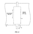
- FIG. 2 is a top view of an exemplary embodiment of a bias charge roller illustrating the process direction.
- FIG. 3 illustrates an exemplary image forming apparatus of the present disclosure.
- FIG. 4 is a graph showing the charge uniformity testing of a conventional bias charge roller lacking an overcoat layer.
- FIG. 5 is a graph showing the charge uniformity testing of a bias charge roller fabricated with an overcoat layer.
- FIG. 6 illustrates a print image from a control imaging apparatus after 50,000 cycles wherein the bias charge roller does not have an overcoat layer.
- FIG. 7 illustrates a print image from an imaging apparatus fabricated with an overcoat layer after 50,000 cycles.
- the modifier “about” used in connection with a quantity is inclusive of the stated value and has the meaning dictated by the context (for example, it includes at least the degree of error associated with the measurement of the particular quantity).
- the modifier “about” should also be considered as disclosing the range defined by the absolute values of the two endpoints. For example, the range of “from about 2 to about 10” also discloses the range “from 2 to 10”.
- the present disclosure relates to overcoat layers that are useful on the bias charge roller of an imaging apparatus.
- the overcoat layers comprise a phenolic resin and a conductive agent. Bias charge rollers containing the overcoat layer are disclosed.
- the present disclosure also relates to a cartridge to be placed in an imaging apparatus.
- the cartridge is useful for applying an electrical charge to an associated imaging member in the imaging apparatus.
- the cartridge comprises (1) a bias charge roller that can be situated in proximity to a surface of the imaging member and (2) a power supply for supplying a voltage to the bias charge roller.
- the bias charge roller comprises an overcoat layer comprised of a phenolic resin and a conductive agent.
- the image forming apparatus comprises an electrophotographic imaging member having a charge-retentive surface to receive an electrostatic latent image thereon, a development component to apply a developer material to the charge-retentive surface to develop the electrostatic latent image to form a developed image on the charge-retentive surface, a transfer component for transferring the developed image from the charge-retentive surface to another member or a copy substrate, a fusing member to fuse the developed image to the copy substrate, and a bias charge roller for applying a charge to the charge-retentive surface.
- the electrophotographic imaging member comprises a substrate, an electrically conductive layer when the substrate is not electrically conductive, a charge generating layer, and a charge transport layer.
- the bias charge roller comprises an overcoat layer comprised of a phenolic resin and a conductive agent.
- FIG. 1 a portion of an image forming apparatus is shown.
- the image forming apparatus has a power supply 10 , an imaging member surface 20 , and a bias charge roller 30 .
- the imaging member may be a drum, a belt, a film, a drelt, or any other type of imaging member.
- the bias charge roller 30 comprises a conductive core and an overcoat layer 36 . As shown here, the conductive core is formed from a core 32 and a conductive layer 34 .
- FIG. 2 is a diagram illustrating the operation of the bias charge roller.
- the bias charge roller rotates about the axis of the core, either under its own power or by friction with the imaging member surface.
- the direction in which the imaging member surface travels is considered the process direction, and corresponds roughly to a radial direction of the bias charge roller itself, or perpendicular to the axis of the core.
- the overcoat layer for the bias charge roller should have a surface resistivity of from 10 5 to 10 13 ohm/sq in order to achieve good print quality.
- the overcoat layer should adhere well to the conductive layer.
- the overcoat layer comprises a phenolic resin and a conductive agent.
- phenolic resin refers to a polymeric resin containing repeating units of a six-membered aromatic ring, i.e. phenyl, directly bonded to a hydroxyl group (—OH).
- the resin may be a homopolymer in some embodiments.
- the phenolic resin may be a formaldehyde polymer generated with phenol, p-tert-butylphenol and cresol; a formaldehyde polymer generated with ammonia, cresol, and phenol; a formaldehyde polymer generated with 4,4′-(1-methylethylidene) bisphenol; a formaldehyde polymer generated with cresol and phenol; a formaldehyde polymer generated with phenol and p-tert-butylphenol; a nitrile phenolic, an epoxy phenolic; and mixtures thereof.
- Exemplary phenolic resins are commercially available as Plyophen J-325 from Dainippon Ink and Chemical, Inc. or Phenolite J-325 from DIC Corp.
- the phenolic resin may comprise from 99.9 to about 60 wt %, or from about 96 to about 91 wt % of the overcoat layer. In particular embodiments, the phenolic resin comprises about 95 wt % of the overcoat layer.
- the conductive agent of the overcoat layer is generally in the form of conductive particles.
- the conductive agent may be a metal or a metal oxide.
- the metal of the metal oxide may generally be any conductive metal which can be oxidized.
- the metal may be titanium (Ti), tin (Sn), zinc (Zn), indium (In), silicon (Si), aluminum (Al), zirconium (Zr), or molybdenum (Mb).
- the conductive particles may alternatively be made from ammonium perchlorates or chlorates, alkali metal perchlorates or chlorates, conductive polymers like polyaniline, polypyrrole, polythiophene, and polyacetylene, and the like.
- the conductive agent is carbon black.
- Carbon black is a virtually pure elemental carbon in the form of colloidal particles that are produced by incomplete combustion or thermal decomposition of gaseous or liquid hydrocarbons under controlled conditions. Its appearance is that of a black, finely divided pellet or powder. Carbon black is chemically distinct from soot and black carbon. Carbon black generally contains at least 97 wt % elemental carbon arranged as aciniform (grape-like cluster) particulates.
- the carbon black may be VULCAN® XC72, available from Cabot Corporation, which possesses a density of 264 kg/m 3 and an oil absorption number (OAN) of 174 cc/100 g.
- the conductive agent may comprise from 0.1 to about 40 wt %, or from about 4 to about 9 wt % of the overcoat layer. In particular embodiments, the conductive agent comprises about 5 wt % of the overcoat layer.
- the overcoat layer may have a thickness of from about 0.1 ⁇ m to about 500 ⁇ m, or from about 1 ⁇ m to about 50 ⁇ m. In particular embodiments, the overcoat layer has a thickness of from 1 ⁇ m to 15 ⁇ m, including about 5 ⁇ m.
- the overcoat layer may be applied by any suitable conventional technique such as spraying, dip coating, draw bar coating, gravure coating, silk screening, air knife coating, reverse roll coating, vacuum deposition, chemical treatment and the like.
- the overcoat layer is preferably applied in the form of a dispersion or solution, where the phenolic resin and conductive particles are dispersed or dissolved in a solvent.
- Suitable solvents include xylene, 1-butanol, methyl ethyl ketone, and the like and mixtures thereof.
- the order in which the ingredients are added to the solution/dispersion is not important.
- the solution/dispersion can be deposited by conventional techniques such as by vacuum, heating and the like.
- the solvent is removed after deposition of the solution/dispersion by conventional techniques such as by vacuum, heating and the like.
- the overcoat layer may be cured or dried at a temperature of from about 40 to about 200° C. for a suitable period of time, such as from about 1 minute to about 10 hours, under stationary conditions or in an air flow.
- the core 32 of the bias charge roller is used to support the bias charge roller, and may generally be made up of any conductive material. Exemplary materials include aluminum, iron, copper, or stainless steel.
- the shape of the core may be cylindrical, tubular, or any other suitable shape.
- the core may have a length of from 200 mm to 700 mm.
- the diameter of the core may be from about 1 mm to about 20 cm, or from about 5 mm to about 2 cm.
- the conductive layer 34 of the bias charge roller surrounds the core 32 .
- the conductive layer comprises a polymeric material such as, for example, neoprene, EPDM rubber, nitrile rubber, polyurethane rubber (polyester type), polyurethane rubber (polyether type), silicone rubber, VITON/FLUOREL rubber, epichlorohydrin rubber, or other similar materials having a DC volume resistivity in the range of 10 3 to 10 7 ohm-cm after suitable compounding with a conductive filler such as carbon particles, graphite, pyrolytic carbon, metal oxides, ammonium perchlorates or chlorates, alkali metal perchlorates or chlorates, conductive polymers like polyaniline, polypyrrole, polythiophene, and polyacetylene, and the like.
- a conductive filler such as carbon particles, graphite, pyrolytic carbon, metal oxides, ammonium perchlorates or chlorates, alkali metal perchlorates or chlor
- the conductive filler may be present in the amount of from about 1 to about 30 parts by weight per 100 parts by weight of the polymeric material. Desirably, the conductive layer is deformable to ensure close proximity or contact with the imaging member surface.
- the Shore O hardness is typically from about 15 to about 80.
- the elastomer may be, for example, urethane rubber, epichlorohydrin elastomers, EPDM rubbers, styrene butadiene rubbers, fluoro-elastomers, silicone rubbers, or any other suitable material.
- the conductive layer may have any suitable thickness such as, for example, about 10 mm to about 20 cm, preferably from about 50 mm to about 3 cm. It is also possible to use a stiff, non-conformable conductive layer.
- the power supply 10 may connect to the bias charge roller 30 via the core 32 .
- the voltage provided by the power supply may be a standard line voltage or other voltage levels or signal frequencies which may be desirable in accordance with other limiting factors dependent upon the individual machine design.
- the power supply may provide a DC voltage, an AC voltage, or variations thereof.
- the bias charge roller may be provided in the form of a cartridge for easy insertion and removal from the image forming apparatus.
- the cartridge 40 contains the bias charge roller 30 .
- a power interface 42 exists to connect the bias charge roller 30 to the power supply 10 of the image forming apparatus and supply voltage to the bias charge roller.
- a cleaning member 50 may also be present to remove toner, paper dust, lubricant, etc. that is transferred from the imaging member surface 20 to the bias charge roller 30 .
- the cleaning member may be, for example, a felt, sponge, etc., and may be shaped as, for example, a roller, a plate, or a sheet.
- the overcoat layer of the present disclosure improves the lifetime of the bias charge roller and has improved print properties over time, i.e. it does not produce dark streaks.
- the overcoated bias charge roller also displays excellent charge uniformity.
- the overcoat layer also allows for refurbishing of a used bias charge roller; after applying the overcoat layer to the damaged surface, the bias charge roller can continue to be used.
- the bias charge roller may be used in an image forming apparatus that forms images on a recording medium, such as that shown in FIG. 3 .
- Such an image forming apparatus comprises an electrophotographic imaging member, a development component, a transfer component, and a fusing member.
- the electrophotographic imaging member has a charge-retentive surface to receive an electrostatic latent image thereon.
- the electrophotographic imaging member generally comprises a substrate, an electrically conductive layer when the substrate is not electrically conductive, a charge generating layer, and a charge transport layer. Imaging members are known in the art.
- the bias charge roller applies a uniform charge to the charge-retentive surface.
- the development component applies a developer material, i.e.
- the transfer component transfers the developed image from the charge-retentive surface to another member or a copy substrate, such as paper.
- the fusing member fuses the developed image to the copy substrate.
- the charge-retentive surface of imaging member 110 is charged by bias charge roller 112 to which a voltage has been supplied from power supply 111 .
- the imaging member is then imagewise exposed to light from an optical system or an image input apparatus 113 , such as a laser and light emitting diode, to form an electrostatic latent image thereon.
- an optical system or an image input apparatus 113 such as a laser and light emitting diode
- the electrostatic latent image is developed by bringing a developer mixture from developer station 114 into contact therewith. Development can be effected by use of a magnetic brush, powder cloud, or other known development process.
- a dry developer mixture usually comprises carrier granules having toner particles adhering triboelectrically thereto.
- Toner particles are attracted from the carrier granules to the latent image forming a toner powder image thereon.
- a liquid developer material may be employed, which includes a liquid carrier having toner particles dispersed therein.
- the liquid developer material is advanced into contact with the electrostatic latent image and the toner particles are deposited thereon. After the toner particles have been deposited on the photoconductive surface, they are transferred to a copy substrate 116 by transfer component 115 , which can be pressure transfer or electrostatic transfer.
- the developed image can be transferred to an intermediate transfer member, or bias transfer member, and subsequently transferred to a copy substrate.
- copy substrates include paper, transparency material such as polyester, polycarbonate, or the like, cloth, wood, or any other desired material upon which the finished image will be situated.
- copy substrate 116 advances to fusing member 119 , depicted as fuser belt 120 and pressure roll 121 , wherein the developed image is fused to copy substrate 116 by passing the copy substrate between the fuser belt and pressure roll, thereby forming a permanent image.
- transfer and fusing can be effected by a transfix application.
- the imaging member 110 then advances to cleaning station 117 , wherein any remaining toner is cleaned therefrom by use of a blade (as shown in FIG. 1 ), brush, or other cleaning apparatus.
- a bias charge roller without an overcoat layer was used for comparison.
- the bias charge roller was then cycled 50,000 times in a Hodaka wear rate fixture.
- the bias charge roller was also print tested in a copier after the wear testing.
- An overcoat dispersion was prepared by ball milling a sample of Plyophen J-325 phenolic resin (available from Dainippon Ink and Chemicals, Inc.) with VULCAN® XC72 carbon black (available from Cabot Corporation) in a 50:50 mixture of xylene and butanol. The sample was ball milled for 3 days, after which the dispersion was filtered. A 5 ⁇ m overcoat layer was coated on a bias charge roller identical to the one used in Comparative Example 1 using a Tsukiage coater. The bias charge roller was then dried in a convection oven for 15 minutes at 140° C. to remove the solvent and cure the overcoat. The resulting overcoat layer was 5 wt % carbon black and 95 wt % phenolic resin. The surface resistivity of the material was measured to be 10 8 ⁇ /sq.
- the charge uniformity tests for Comparative Example 1 are shown in FIG. 4
- the charge uniformity tests for Example 1 are shown in FIG. 5 .
- 0 refers to one end of the roller
- 328 refers to the other end of the roller.
- the potential for Comparative Example 1 is a relatively straight line between the ends of the roller, both before and after the wear testing.
- the potential for Example 1 is also a relatively straight line between the ends of the roller, both before and after the wear testing. This indicated that there was no electrical charge build-up in the overcoat layers and no deterioration of charge capacity, i.e.
- FIG. 6 shows the results of the print testing for the bias charge roller of Comparative Example 1
- FIG. 7 shows the results of the print testing for Example 1.
- the bias charge roller of Comparative Example 1 showed significant streaking.
- no print defects were observed in the bias charge roller of Example 1. This indicated that the bias charge roller of Comparative Example 1 sustained significant wear while the overcoat layer improved the wear resistance of the bias charge roller of Example 1.
Landscapes
- Physics & Mathematics (AREA)
- Engineering & Computer Science (AREA)
- Plasma & Fusion (AREA)
- General Physics & Mathematics (AREA)
- Electrostatic Charge, Transfer And Separation In Electrography (AREA)
- Rolls And Other Rotary Bodies (AREA)
Abstract
Description
Claims (17)
Priority Applications (1)
| Application Number | Priority Date | Filing Date | Title |
|---|---|---|---|
| US12/706,951 US8086142B2 (en) | 2010-02-17 | 2010-02-17 | Bias charge roller comprising overcoat layer |
Applications Claiming Priority (1)
| Application Number | Priority Date | Filing Date | Title |
|---|---|---|---|
| US12/706,951 US8086142B2 (en) | 2010-02-17 | 2010-02-17 | Bias charge roller comprising overcoat layer |
Publications (2)
| Publication Number | Publication Date |
|---|---|
| US20110200361A1 US20110200361A1 (en) | 2011-08-18 |
| US8086142B2 true US8086142B2 (en) | 2011-12-27 |
Family
ID=44369739
Family Applications (1)
| Application Number | Title | Priority Date | Filing Date |
|---|---|---|---|
| US12/706,951 Expired - Fee Related US8086142B2 (en) | 2010-02-17 | 2010-02-17 | Bias charge roller comprising overcoat layer |
Country Status (1)
| Country | Link |
|---|---|
| US (1) | US8086142B2 (en) |
Cited By (2)
| Publication number | Priority date | Publication date | Assignee | Title |
|---|---|---|---|---|
| US9063509B2 (en) | 2013-07-11 | 2015-06-23 | Xerox Corporation | Coating apparatuses and methods |
| US10768553B2 (en) | 2017-04-18 | 2020-09-08 | Hp Indigo B.V. | Layers for resistance to adhesion of ink |
Families Citing this family (4)
| Publication number | Priority date | Publication date | Assignee | Title |
|---|---|---|---|---|
| JP5950875B2 (en) * | 2013-07-22 | 2016-07-13 | 京セラドキュメントソリューションズ株式会社 | Charging roller, image forming device |
| JP6464718B2 (en) * | 2014-12-17 | 2019-02-06 | 株式会社リコー | Image forming apparatus |
| JP6883203B2 (en) * | 2017-03-06 | 2021-06-09 | 富士フイルムビジネスイノベーション株式会社 | Conductive rolls, transfer rolls, process cartridges, and image forming equipment |
| JP7046598B2 (en) * | 2017-12-26 | 2022-04-04 | キヤノン株式会社 | Manufacturing method of charged member |
Citations (14)
| Publication number | Priority date | Publication date | Assignee | Title |
|---|---|---|---|---|
| US3684364A (en) | 1971-06-24 | 1972-08-15 | Xerox Corp | Lift off electrode |
| JPH03284770A (en) * | 1990-03-31 | 1991-12-16 | Tokai Rubber Ind Ltd | Conductive roll |
| JPH04284475A (en) * | 1991-03-13 | 1992-10-09 | Tokai Rubber Ind Ltd | Electrical conductive roll |
| JPH05265311A (en) * | 1992-03-23 | 1993-10-15 | Tokai Rubber Ind Ltd | Conductive roll |
| JPH0792774A (en) * | 1993-09-22 | 1995-04-07 | Bridgestone Corp | Charging member and charger |
| US5613173A (en) | 1995-12-22 | 1997-03-18 | Xerox Corporation | Biased roll charging apparatus having clipped AC input voltage |
| JPH10115977A (en) * | 1996-10-08 | 1998-05-06 | Bridgestone Corp | Development assistant member, and developing device |
| US6807389B2 (en) | 2002-12-13 | 2004-10-19 | Xerox Corporation | Bias charge roller with optimally induced AC corona |
| US6842594B2 (en) | 2002-12-13 | 2005-01-11 | Xerox Corporation | Intermittent DC bias charge roll AC cleaning cycle |
| US7103304B2 (en) * | 2003-06-26 | 2006-09-05 | Fuji Xerox Co., Ltd. | Electrically conductive member, unit for cleaning image holding member, process cartridge and image forming apparatus |
| US7177572B2 (en) | 2004-06-25 | 2007-02-13 | Xerox Corporation | Biased charge roller with embedded electrodes with post-nip breakdown to enable improved charge uniformity |
| US7623812B2 (en) | 2006-04-28 | 2009-11-24 | Sharp Kabushiki Kaisha | Image forming apparatus, charging roller, production method of charging roller, production apparatus of charging roller |
| US20110045305A1 (en) * | 2009-08-24 | 2011-02-24 | Xerox Corporation | Treatment of carbon black with a fluorosilane |
| US7912411B2 (en) * | 2004-06-09 | 2011-03-22 | Bridgestone Corporation | Developing roller and imaging apparatus using the same |
-
2010
- 2010-02-17 US US12/706,951 patent/US8086142B2/en not_active Expired - Fee Related
Patent Citations (14)
| Publication number | Priority date | Publication date | Assignee | Title |
|---|---|---|---|---|
| US3684364A (en) | 1971-06-24 | 1972-08-15 | Xerox Corp | Lift off electrode |
| JPH03284770A (en) * | 1990-03-31 | 1991-12-16 | Tokai Rubber Ind Ltd | Conductive roll |
| JPH04284475A (en) * | 1991-03-13 | 1992-10-09 | Tokai Rubber Ind Ltd | Electrical conductive roll |
| JPH05265311A (en) * | 1992-03-23 | 1993-10-15 | Tokai Rubber Ind Ltd | Conductive roll |
| JPH0792774A (en) * | 1993-09-22 | 1995-04-07 | Bridgestone Corp | Charging member and charger |
| US5613173A (en) | 1995-12-22 | 1997-03-18 | Xerox Corporation | Biased roll charging apparatus having clipped AC input voltage |
| JPH10115977A (en) * | 1996-10-08 | 1998-05-06 | Bridgestone Corp | Development assistant member, and developing device |
| US6807389B2 (en) | 2002-12-13 | 2004-10-19 | Xerox Corporation | Bias charge roller with optimally induced AC corona |
| US6842594B2 (en) | 2002-12-13 | 2005-01-11 | Xerox Corporation | Intermittent DC bias charge roll AC cleaning cycle |
| US7103304B2 (en) * | 2003-06-26 | 2006-09-05 | Fuji Xerox Co., Ltd. | Electrically conductive member, unit for cleaning image holding member, process cartridge and image forming apparatus |
| US7912411B2 (en) * | 2004-06-09 | 2011-03-22 | Bridgestone Corporation | Developing roller and imaging apparatus using the same |
| US7177572B2 (en) | 2004-06-25 | 2007-02-13 | Xerox Corporation | Biased charge roller with embedded electrodes with post-nip breakdown to enable improved charge uniformity |
| US7623812B2 (en) | 2006-04-28 | 2009-11-24 | Sharp Kabushiki Kaisha | Image forming apparatus, charging roller, production method of charging roller, production apparatus of charging roller |
| US20110045305A1 (en) * | 2009-08-24 | 2011-02-24 | Xerox Corporation | Treatment of carbon black with a fluorosilane |
Non-Patent Citations (1)
| Title |
|---|
| "What is Carbon Black" International Carbon Black Association, 2008, http://www.carbon-black.org/what-is.html, accessed Feb. 16, 2010, 2 pgs. |
Cited By (2)
| Publication number | Priority date | Publication date | Assignee | Title |
|---|---|---|---|---|
| US9063509B2 (en) | 2013-07-11 | 2015-06-23 | Xerox Corporation | Coating apparatuses and methods |
| US10768553B2 (en) | 2017-04-18 | 2020-09-08 | Hp Indigo B.V. | Layers for resistance to adhesion of ink |
Also Published As
| Publication number | Publication date |
|---|---|
| US20110200361A1 (en) | 2011-08-18 |
Similar Documents
| Publication | Publication Date | Title |
|---|---|---|
| CN110780560B (en) | Electrophotographic member, process cartridge, and electrophotographic image forming apparatus | |
| US9494888B2 (en) | Imaging device components comprised of hydrophobic carbon nanotubes | |
| US8086142B2 (en) | Bias charge roller comprising overcoat layer | |
| JP6641828B2 (en) | Charging member, image forming apparatus and process cartridge | |
| CN1017752B (en) | charger | |
| CN111258197B (en) | Developing member, electrophotographic process cartridge, and electrophotographic image forming apparatus | |
| US8768219B2 (en) | Bias charging overcoat | |
| JP7499336B2 (en) | CONDUCTIVE ROLL INSPECTION METHOD AND CONDUCTIVE ROLL MANUFACTURING METHOD | |
| US20110201485A1 (en) | Bias charge roller comprising overcoat layer | |
| US5881343A (en) | Charging method and charging device | |
| US8249488B2 (en) | Bias charge roller comprising overcoat layer | |
| US20230229097A1 (en) | Charging member, charging device, image forming apparatus, and process cartridge | |
| US5666607A (en) | Wet contact charging for electrophotography | |
| JP2024013572A (en) | Image forming device, image forming method using the same, and charging device | |
| US6629915B1 (en) | Semi-conducting roll and developing device | |
| JP3347623B2 (en) | Charging device and electrophotographic device | |
| US8649704B2 (en) | Bias charging overcoat | |
| EP1178364A1 (en) | Conductive member, process cartridge and electrophotographic apparatus | |
| KR20080049600A (en) | Charging apparatus, image forming apparatus and image forming unit using the same | |
| JP3313996B2 (en) | Charging device and electrophotographic device | |
| JP7358207B2 (en) | Developing member, electrophotographic process cartridge, and electrophotographic image forming device | |
| JP4289928B2 (en) | Method for manufacturing conductive member | |
| EP4184025A1 (en) | Conductive roller | |
| JP3423143B2 (en) | Charging member and method of manufacturing the same | |
| JP2005099763A (en) | Image forming apparatus |
Legal Events
| Date | Code | Title | Description |
|---|---|---|---|
| AS | Assignment |
Owner name: XEROX CORPORATION, CONNECTICUT Free format text: ASSIGNMENT OF ASSIGNORS INTEREST;ASSIGNORS:GILMARTIN, BRIAN P.;LIN, LIANG-BIH;KOVAL, JEANNE M.;AND OTHERS;REEL/FRAME:023946/0354 Effective date: 20100212 |
|
| FEPP | Fee payment procedure |
Free format text: PAYOR NUMBER ASSIGNED (ORIGINAL EVENT CODE: ASPN); ENTITY STATUS OF PATENT OWNER: LARGE ENTITY |
|
| ZAAA | Notice of allowance and fees due |
Free format text: ORIGINAL CODE: NOA |
|
| ZAAB | Notice of allowance mailed |
Free format text: ORIGINAL CODE: MN/=. |
|
| STCF | Information on status: patent grant |
Free format text: PATENTED CASE |
|
| FPAY | Fee payment |
Year of fee payment: 4 |
|
| MAFP | Maintenance fee payment |
Free format text: PAYMENT OF MAINTENANCE FEE, 8TH YEAR, LARGE ENTITY (ORIGINAL EVENT CODE: M1552); ENTITY STATUS OF PATENT OWNER: LARGE ENTITY Year of fee payment: 8 |
|
| AS | Assignment |
Owner name: CITIBANK, N.A., AS AGENT, DELAWARE Free format text: SECURITY INTEREST;ASSIGNOR:XEROX CORPORATION;REEL/FRAME:062740/0214 Effective date: 20221107 |
|
| AS | Assignment |
Owner name: XEROX CORPORATION, CONNECTICUT Free format text: RELEASE OF SECURITY INTEREST IN PATENTS AT R/F 062740/0214;ASSIGNOR:CITIBANK, N.A., AS AGENT;REEL/FRAME:063694/0122 Effective date: 20230517 |
|
| AS | Assignment |
Owner name: CITIBANK, N.A., AS COLLATERAL AGENT, NEW YORK Free format text: SECURITY INTEREST;ASSIGNOR:XEROX CORPORATION;REEL/FRAME:064760/0389 Effective date: 20230621 |
|
| FEPP | Fee payment procedure |
Free format text: MAINTENANCE FEE REMINDER MAILED (ORIGINAL EVENT CODE: REM.); ENTITY STATUS OF PATENT OWNER: LARGE ENTITY |
|
| AS | Assignment |
Owner name: JEFFERIES FINANCE LLC, AS COLLATERAL AGENT, NEW YORK Free format text: SECURITY INTEREST;ASSIGNOR:XEROX CORPORATION;REEL/FRAME:065628/0019 Effective date: 20231117 |
|
| LAPS | Lapse for failure to pay maintenance fees |
Free format text: PATENT EXPIRED FOR FAILURE TO PAY MAINTENANCE FEES (ORIGINAL EVENT CODE: EXP.); ENTITY STATUS OF PATENT OWNER: LARGE ENTITY |
|
| STCH | Information on status: patent discontinuation |
Free format text: PATENT EXPIRED DUE TO NONPAYMENT OF MAINTENANCE FEES UNDER 37 CFR 1.362 |
|
| AS | Assignment |
Owner name: XEROX CORPORATION, CONNECTICUT Free format text: TERMINATION AND RELEASE OF SECURITY INTEREST IN PATENTS RECORDED AT RF 064760/0389;ASSIGNOR:CITIBANK, N.A., AS COLLATERAL AGENT;REEL/FRAME:068261/0001 Effective date: 20240206 Owner name: CITIBANK, N.A., AS COLLATERAL AGENT, NEW YORK Free format text: SECURITY INTEREST;ASSIGNOR:XEROX CORPORATION;REEL/FRAME:066741/0001 Effective date: 20240206 |
|
| FP | Lapsed due to failure to pay maintenance fee |
Effective date: 20231227 |