US8085357B2 - Liquid crystal display - Google Patents
Liquid crystal display Download PDFInfo
- Publication number
- US8085357B2 US8085357B2 US12/051,757 US5175708A US8085357B2 US 8085357 B2 US8085357 B2 US 8085357B2 US 5175708 A US5175708 A US 5175708A US 8085357 B2 US8085357 B2 US 8085357B2
- Authority
- US
- United States
- Prior art keywords
- liquid crystal
- crystal display
- mold frame
- side wall
- bezel
- Prior art date
- Legal status (The legal status is an assumption and is not a legal conclusion. Google has not performed a legal analysis and makes no representation as to the accuracy of the status listed.)
- Expired - Fee Related, expires
Links
Images


Classifications
-
- G—PHYSICS
- G02—OPTICS
- G02F—OPTICAL DEVICES OR ARRANGEMENTS FOR THE CONTROL OF LIGHT BY MODIFICATION OF THE OPTICAL PROPERTIES OF THE MEDIA OF THE ELEMENTS INVOLVED THEREIN; NON-LINEAR OPTICS; FREQUENCY-CHANGING OF LIGHT; OPTICAL LOGIC ELEMENTS; OPTICAL ANALOGUE/DIGITAL CONVERTERS
- G02F1/00—Devices or arrangements for the control of the intensity, colour, phase, polarisation or direction of light arriving from an independent light source, e.g. switching, gating or modulating; Non-linear optics
- G02F1/01—Devices or arrangements for the control of the intensity, colour, phase, polarisation or direction of light arriving from an independent light source, e.g. switching, gating or modulating; Non-linear optics for the control of the intensity, phase, polarisation or colour
- G02F1/13—Devices or arrangements for the control of the intensity, colour, phase, polarisation or direction of light arriving from an independent light source, e.g. switching, gating or modulating; Non-linear optics for the control of the intensity, phase, polarisation or colour based on liquid crystals, e.g. single liquid crystal display cells
- G02F1/133—Constructional arrangements; Operation of liquid crystal cells; Circuit arrangements
- G02F1/1333—Constructional arrangements; Manufacturing methods
- G02F1/133308—Support structures for LCD panels, e.g. frames or bezels
-
- G—PHYSICS
- G02—OPTICS
- G02F—OPTICAL DEVICES OR ARRANGEMENTS FOR THE CONTROL OF LIGHT BY MODIFICATION OF THE OPTICAL PROPERTIES OF THE MEDIA OF THE ELEMENTS INVOLVED THEREIN; NON-LINEAR OPTICS; FREQUENCY-CHANGING OF LIGHT; OPTICAL LOGIC ELEMENTS; OPTICAL ANALOGUE/DIGITAL CONVERTERS
- G02F1/00—Devices or arrangements for the control of the intensity, colour, phase, polarisation or direction of light arriving from an independent light source, e.g. switching, gating or modulating; Non-linear optics
- G02F1/01—Devices or arrangements for the control of the intensity, colour, phase, polarisation or direction of light arriving from an independent light source, e.g. switching, gating or modulating; Non-linear optics for the control of the intensity, phase, polarisation or colour
- G02F1/13—Devices or arrangements for the control of the intensity, colour, phase, polarisation or direction of light arriving from an independent light source, e.g. switching, gating or modulating; Non-linear optics for the control of the intensity, phase, polarisation or colour based on liquid crystals, e.g. single liquid crystal display cells
- G02F1/133—Constructional arrangements; Operation of liquid crystal cells; Circuit arrangements
- G02F1/1333—Constructional arrangements; Manufacturing methods
- G02F1/133308—Support structures for LCD panels, e.g. frames or bezels
- G02F1/133314—Back frames
-
- G—PHYSICS
- G02—OPTICS
- G02F—OPTICAL DEVICES OR ARRANGEMENTS FOR THE CONTROL OF LIGHT BY MODIFICATION OF THE OPTICAL PROPERTIES OF THE MEDIA OF THE ELEMENTS INVOLVED THEREIN; NON-LINEAR OPTICS; FREQUENCY-CHANGING OF LIGHT; OPTICAL LOGIC ELEMENTS; OPTICAL ANALOGUE/DIGITAL CONVERTERS
- G02F1/00—Devices or arrangements for the control of the intensity, colour, phase, polarisation or direction of light arriving from an independent light source, e.g. switching, gating or modulating; Non-linear optics
- G02F1/01—Devices or arrangements for the control of the intensity, colour, phase, polarisation or direction of light arriving from an independent light source, e.g. switching, gating or modulating; Non-linear optics for the control of the intensity, phase, polarisation or colour
- G02F1/13—Devices or arrangements for the control of the intensity, colour, phase, polarisation or direction of light arriving from an independent light source, e.g. switching, gating or modulating; Non-linear optics for the control of the intensity, phase, polarisation or colour based on liquid crystals, e.g. single liquid crystal display cells
- G02F1/133—Constructional arrangements; Operation of liquid crystal cells; Circuit arrangements
- G02F1/1333—Constructional arrangements; Manufacturing methods
- G02F1/133308—Support structures for LCD panels, e.g. frames or bezels
- G02F1/133322—Mechanical guidance or alignment of LCD panel support components
Definitions
- the present invention relates to a liquid crystal display, and more particularly, to a liquid crystal display having increased structural integrity.
- a liquid crystal display is one of various flat panel display (FPD) devices that display images using liquid crystal. Because the LCD is thin, lightweight, and has low drive voltage and low power consumption as compared to other display devices, LCDs have been widely used in every industrial field.
- the LCD includes a thin film transistor (TFT) substrate, a color filter facing to the thin film transistor substrate and a liquid crystal display panel having liquid crystals between the two substrates that change its optical transmission efficiency by applying an electrical signal.
- TFT thin film transistor
- the liquid crystal display panel requires a light source that provides lights having brightness higher than a threshold level to the liquid crystal display panel for displaying images because the liquid crystal does not emit light itself.
- the back light unit includes a light guide plate for collecting light generated from the light emitting diode as a light source to the liquid display panel, and optical sheets that make the light emitted from the light guide plate uniform and convert a progress path of the light so as to obtain optimum brightness.
- the light guide plate and the optical sheets are stacked from top to bottom in the back light unit.
- the liquid crystal display panel and the back light unit are generally supported by a mold frame and a bezel.
- the liquid crystal display panel and the back light unit are assembled to be attached to a resin mold frame made by a hook method.
- a metal bezel surrounds a periphery of the mold frame to maintain the strength of the mold frame.
- the mold frame and bezel structure has become smaller as devices such as cellular phones, Portable Multimedia Players (PMP), and digital cameras have become thinner and more lightweight.
- the mold frame and bezel structure there are limitations to miniaturization of the mold frame and bezel structure. For example, if the bezel becomes too thin, the structural integrity is weakened, thereby being easily deformed by torsion force caused by external impact. Accordingly, the mold frame may deform, thereby damaging the back light unit and the liquid crystal display.
- An aspect of an embodiment of the present invention is directed toward a liquid crystal display that can improve torsion strength by including a bezel formed by a double drawing process.
- a liquid crystal display in an embodiment of the present invention, includes a liquid crystal display panel, a back light unit attached to the liquid crystal display panel having a light source and a light guide plate, a mold frame attached to the back light unit, and a bezel within the mold frame for supporting the mold frame.
- the bezel includes a first seat having a base extending in a first direction and a first side wall extending from a perimeter of the base in a second direction substantially perpendicular to a first direction, and a second seat having a step extending from the first side wall in a third direction substantially parallel to the first direction and a second side extending from a perimeter of the step in a fourth direction substantially perpendicular to the third direction.
- the mold frame is seated within the first seat and the first side wall surrounds a lateral surface of the mold frame.
- the liquid crystal display panel may be seated in the second seat, and the second side wall may surround a lateral surface of the liquid crystal display panel.
- the mold frame may include a mold frame rib extending along the second side wall and the step.
- the first seat may further include a flange extending along one side edge of the base of the mold frame.
- the mold frame further includes a mold frame insert extending along an exterior edge of the step and the second side wall, wherein an exposed edge of the mold frame insert is aligned with the base and another exposed edge of the mold frame insert is aligned with the second side wall.
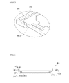
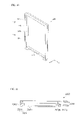
- FIG. 1 is a combined schematic of a liquid crystal display (LCD) according to an exemplary embodiment of the present invention.
- LCD liquid crystal display
- FIG. 2 is an exploded perspective schematic of the LCD of FIG. 1 .
- FIG. 3 is a partial perspective detail schematic of region “A” of the LCD of FIG. 2 .
- FIG. 4 is a sectional schematic of a frame structure taken along B-B′ line of FIG. 2 .
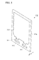
- FIG. 5 is a perspective schematic of a mold frame according to another exemplary embodiment of the present invention.
- FIG. 6 is a perspective schematic of a bezel according to yet another exemplary embodiment of the present invention.
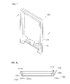
- FIG. 7 is a perspective schematic of a mold frame and a bezel according to yet another exemplary embodiment of the present invention.
- FIG. 8 a is a sectional schematic taken along C-C′ line of FIG. 7 .
- FIG. 8 b is a sectional schematic of a light guide plate and an LCD panel seated in the combined structure of FIG. 8 a.
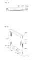
- FIG. 9 is a perspective schematic of the mold frame according to another exemplary embodiment of the present invention.
- FIG. 10 is a perspective schematic of the bezel according to another exemplary embodiment of the present invention.
- FIG. 11 is a sectional schematic of the frame structure according to still another exemplary embodiment of the present invention.
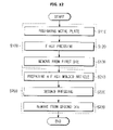
- FIG. 12 is a flow chart of a method of producing the bezel according to an exemplary embodiment of the present invention.
- FIGS. 13 a , 13 b , 13 c , 13 d , 13 e , and 13 f are sectional schematics of the method steps according to the flow chart of FIG. 12 .
- an LCD 1 includes a liquid crystal panel 100 , a back light unit 200 and a frame structure 300 .
- the frame structure 300 includes a mold frame 310 and a bezel 320 .
- the bezel 320 may be processed by double drawing to have a stepped configuration, and then inserted into the mold frame 310 .
- the liquid crystal panel 100 includes a liquid crystal between two substrates 110 , 120 facing each other, an electrode for driving the liquid crystal, and a polarizing plate arranged on at least one of the two substrates 110 , 120 .
- a drive chip 130 for driving the liquid crystal panel 100 is installed on one side of a lower substrate 120 .
- Information is displayed on a screen of the liquid crystal panel 100 and the liquid crystal panel 100 can be seated within the frame structure 300 .
- the liquid crystal panel 100 may be used, as will be appreciated by one of ordinary skill in the art.
- the back light unit 200 may be located on a back surface of the liquid crystal display panel 100 for providing light required for displaying information on the liquid crystal display panel 100 .
- the back light unit 200 may include a light source 210 , a light guide plate 220 , a reflection sheet 230 , and an optical sheet 240 .
- the light source 210 is arranged at the back surface of the liquid crystal display panel 100 and may be installed in a printed circuit board (PCB) 211 to be electrically coupled to the liquid crystal display panel 100 .
- a printed circuit board (PCB) 211 may be used as the light source 210 .
- the light source 210 provides the liquid crystal display panel 100 with light for displaying image information on the liquid crystal display panel 100 .
- the PCB 211 electrically coupled to the light source 210 may be composed of flexible material to allow easy installation onto the liquid crystal display and may include a plurality of drive chips for driving the light source 210 .
- the light guide plate 220 is located between the light source 210 and the liquid crystal display panel 100 to convert a point light source from the light source 210 to a surface light source.
- the incident light from the light source 210 is scattered onto the back surface 220 a of the light guide plate 220 and travels to the liquid crystal display panel 100 .
- the light guide plate 220 may be composed of a high tensile strength material having a high light transmission efficiency, for example, poly methyl methacrylate (PMMA).
- PMMA poly methyl methacrylate
- the light guide plate 220 is attached to the frame structure 300 as described in more detail below and fixed by the frame structure 300 .
- the reflection sheet 230 may be located on the back surface 220 a of the light guide plate 220 to reduce the light to be transmitted to the liquid crystal display panel 100 from leaking out of the back surface 220 a of the light guide plate 220 . Further, various optical sheets 240 may be located on a front surface 220 b of the light guide plate 220 to improve light transmission efficiency of the liquid crystal display panel 100 .
- the reflection sheet 230 may be arranged at the back surface 200 a of the light guide plate 220 so as to be seated in the frame structure 300 , and more particularly, in the mold frame 310 . As described above, the reflection sheet 230 enables light to be reflected back to the light guide plate 220 .
- the reflection sheet 230 may be made of polyethylene terephthalate (PET) and/or polycarbonate (PC). As one of ordinary skill in the art will appreciate, other suitable material having high reflectivity may be used instead or in addition.
- the optical sheet 240 may include a diffusion sheet 241 for scattering light and uniformly transferring light to the LCD panel, and a prism sheet 242 for enhancing the brightness of the light by focusing the light dispersed by the light guide plate 220 and the diffusion sheet 241 on the LCD panel.
- the back light unit 200 may further include a protection sheet 243 for protecting the optical sheet 240 from being damaged by external impact or dust.
- the back light unit 200 may further include a light shielding tape 250 for preventing light from leaking out to a part where image information is not displayed on the liquid crystal display panel 100 .
- the light shielding tape 250 may be between the optical sheet 240 and the liquid crystal display panel 100 , and more particularly, on an edge of the back light unit 200 where image information is not displayed.
- the frame structure 300 may include the mold frame 310 on which the light source 210 and light guide plate 220 are inserted and fixed (or attached) and the bezel 320 inserted into the mold frame 310 to support the mold frame 310 .
- the frame structure 300 provides space for installing the LCD panel 100 and the back light unit 200 thereon. Further, the frame structure 300 supports the liquid crystal display panel 100 and the back light unit 200 to prevent (or reduce) the liquid crystal display 100 from being damaged by external impact or vibration.
- the mold frame 310 includes a substantially rectangular shape into which the light source 210 and the light guide plate 220 can be inserted. More particularly, the mold frame 310 may include a light source holder 311 for attachment of the light source 210 and a light guide plate holder 312 for attachment of the light guide plate 220 . The mold frame 310 may further include a plurality of drive chip holders 313 , 314 configured to fix a plurality of drive chips on the printed circuit board 211 for driving the light source 210 .
- the light source holder 311 , the light guide plate holder 312 , and the drive chip holders 313 , 314 may be modified based on the types of light source 210 and light guide plate 220 seated in the mold frame 310 , but are not limited to the ones specifically described herein.
- the mold frame 310 may be composed of a synthetic resin and may be integral with the bezel 320 and, for example, formed by injection molding.
- the mold frame 310 may have a thickness t 1 ranging from about 0.3 mm to about 1.0 mm (or from 0.3 mm to 1.0 mm). If the thickness t 1 of the mold frame 310 is less than 0.3 mm, molding the mold frame 310 and inserting and supporting the light source 210 and the light guide plate 220 therein are difficult. If the thickness t 1 of the mold frame 310 is greater than 1.0 mm, the LCD is too thick.
- the bezel 320 includes a first seat 321 for seating the light guide plate 220 and the mold frame 310 , and a second seat 322 for seating the liquid crystal display panel 100 .
- the first seat 321 and the second seat 322 may be formed by double drawing.
- the first seat 321 may include a substantially flat base 321 a and a first side wall 321 b extending from a perimeter of the base 321 a .
- the base 321 a is substantially rectangular and supports the light guide plate 220 and the mold frame 310 .
- the first side wall 321 b surrounds a lateral surface 310 a of the mold frame 310 for seating the mold frame 310 .
- the first side wall 321 b may have a height h 1 substantially corresponding to the thickness t 1 of the mold frame 310 . More particularly, the first side wall 321 b may be equal to or slightly higher than the thickness t 1 of the mold frame 310 so that the mold frame 310 does not protrude from the first side wall 321 b.
- the first side wall 321 b may be continuous around three sides of the bezel and extend partially along a fourth side, as shown in FIG. 6 , to allow for placement of the light source 210 .
- the first side wall may be continuous around the entire perimeter of the base 321 a if necessary to accommodate the back light unit 200 .
- the second seat 322 may having a stepped configuration including a step 322 a extending outwardly from the first side wall 321 b and a second side wall 322 b extending perpendicularly from the step 322 a .
- the step 322 a supports the liquid crystal display panel 100
- the second side wall 322 b encompasses the lateral surface of the LCD panel 100 .
- the second side wall 322 b has a height h 2 substantially corresponding to the thickness of the LCD panel 100 .
- the step 322 a and second side wall 322 b may be configured to substantially match the first seat 321 .
- the step 322 a and the second side wall 322 b may be continuous around three sides of the perimeter of the base 320 a and partially extend along a fourth side, as shown in FIG. 6 .
- the bezel 320 has a thickness ranging from about 0.1 mm to about 0.3 mm. If the thickness t 2 of the bezel 320 is less than 0.1 mm, supporting the mold frame 310 is difficult because the structural integrity of the bezel 320 is weak. On the other hand, if the thickness t 2 of the bezel 320 is greater than 0.3 mm, the LCD may be too thick and/or heavy.
- the bezel 320 may be composed of a relatively rigid (and/or stiff) material for supporting not only the mold frame 310 , but also for supporting the light source 210 , the light guide plate 220 and the LCD panel 100 . As a result, the bezel 320 protects those elements from impact and/or vibration.
- the frame structure 300 may be formed by injection-molding the bezel 320 using a double drawing process and combining the bezel 320 with the mold frame 310 .
- the double drawing process refers to drawing sequentially, using uniquely-sized dies, as described in more detail below.
- the bezel 320 may be formed by processing a metal plate through primary drawing with a relatively large die and processing the metal plate through secondary drawing with a smaller die.
- the strength of the frame structure 300 and the LCD 1 is improved by double drawing the bezel 320 .
- the bezel 320 integrally includes the base 321 a , the first side wall 321 b , the step 322 a and the second side wall 322 b , the bezel 320 is not easily deformed by impact or vibration and can maintain its shape. Further, due to its relatively large width, the torsion strength of the bezel 320 is enhanced.
- a frame structure 1300 includes a bezel 1320 , a mold frame 1310 encompassed in a first seat 1321 , and a second seat 1322 of the bezel 1320 .
- the mold frame 1310 includes a mold frame base 1310 a having a substantially rectangular shape on which the light source 210 ( FIG. 2 ) and the light guide plate 1220 can be inserted, and a mold frame rib 1310 b extending adjacent a second side wall 1322 a , as described in more detail below.
- the mold frame base 1310 a further includes a light source holder 1311 , a light guide plate holder 1312 , and drive chip holders 1313 , 1314 that are configured to be compatibly arranged with the mold frame base.
- a light source holder 1311 the light guide plate holder 1312 , and drive chip holders 1313 , 1314 can have various suitable shapes, as is well known in the art.
- An LCD panel 1100 may be located on an upper surface of the mold frame base mold frame 1310 a.
- the mold frame rib 1310 b is seated in the second seat 1322 of the bezel 1320 .
- the mold frame rib 1310 b extends continuously around a perimeter of the mold frame base 1310 a except along portion 1310 d where the light source is assembled.
- the mold frame rib 1310 b surrounds sides 1100 a of the LCD panel 1100 to fix the LCD panel 1100 .
- the bezel 1320 may include a first seat 1321 and a second seat 1322 for seating the mold frame 1310 .
- the first seat 1321 includes a substantially flat base 1321 a , a first side wall 1321 b extending substantially in a perpendicular direction from a perimeter of the base 1321 a , and a flange 1321 c extending along a lateral surface 1320 a of the base 1321 a for reinforcing the frame structure.
- the mold frame base 1310 a is seated in the base 1321 a and insert-injected to fix the light guide plate 1220 therein. Additionally, the first side wall 1321 b surrounds a lateral surface 1310 e of the mold frame 1310 .
- the second seat 1322 includes a step 1322 a extending substantially perpendicularly from the first side wall 1321 b and a second side wall 1322 b extending substantially perpendicularly from the step 1322 a .
- the mold frame rib 1310 b is seated in the second seat 1322 and insert-injected therein.
- the first side wall 1321 b surrounds a circumference of the mold frame rib mold frame 1310 b.
- the mold frame rib 1310 b surrounds the LCD panel 1100 and acts as a shock absorber to protect the LCD panel 1100 from impact or vibration. Accordingly, the strength of the LCD can be more improved.
- a frame structure 2300 includes a mold frame 2310 having a mold frame base 1310 a , a mold frame rib 1310 b and a mold frame insert 2310 f , and a bezel 2320 including a first seat 2321 and a second seat 2322 formed by a double drawing process.
- the first seat 2321 may include a first seat base 2321 a and a first seat side wall 2321 b
- the second seat 2322 may include a second seat step 2322 a and a second seat side wall 2322 b.
- the mold frame insert 2310 f is insertable into a space between the outside of the first seat side wall 2321 b and the second seat step 2321 a .
- Two externally exposed edges 2310 g , 2310 h of the mold frame insert 2310 f are substantially aligned with the second side wall 2322 b and the base 2321 a , respectively. Accordingly, the mold frame 2310 and the bezel 2320 can be more easily insert-injected because the bezel 2320 can be inserted into the mold frame 2310 without a separate assembly hole.
- a liquid crystal display according to embodiments of the present invention have improved strength and resistance to external torsion force because a bezel insert-injected into the mold frame is processed by double drawing.
- the bezel may not be insert-injected into the mold frame and may be used instead of the frame structure by itself.
- the method of producing the bezel 320 includes a first drawing process (S 100 ) and a second drawing process (S 200 ).
- the first drawing process (S 100 ) includes preparing a metal plate (S 110 ), a first pressing process (S 120 ), and a first punching process (S 130 ).
- the process S 200 includes preparing a first molded article (S 210 ), a second pressing process (S 220 ), and a second punching process (S 230 ).
- a metal plate 32 provided as a base material of the bezel 320 is placed on an upper surface 33 a of a first die 33 .
- a first punch 34 may be aligned over an upper surface 32 a of the metal plate 32 for molding the metal plate 32 into the first die 33 .
- a knock out unit 35 is located inside the first die 33 for removing the metal plate 32 after the metal plate 32 has been molded.
- the metal plate 32 is pressed or punched into the first die 33 by the first punch 34 to form a certain shape. Accordingly, the metal plate 32 forms a first molded article 32 ′ ( FIG. 13 c ) including a base 32 b and an edge 32 c having shape substantially corresponding to the first punch 34 .
- the first molded article 32 ′ is lifted by a knock out unit 35 .
- the first molded article 32 ′ is placed on an upper surface 33 a of a second die 33 ′ having a smaller opening than the first die 33 .
- a second punch 34 ′ may be aligned above an upper surface 32 f of the first molded article 32 ′ for punching the first molded article 32 ′ into the second die 33 ′.
- the first molded article 32 ′ may be fixed by a holder 36 corresponding to and surrounding the edges 32 e of the molded article 32 ′, the holder preventing (or protecting) the molded article from being unnecessarily or undesirably deformed and may be formed in the shape corresponding to a side 32 e of the first molded article 32 ′ so as to surround the side surface 32 e .
- a knock out unit 35 ′ may be located inside the second die 33 ′ to lift the first molded article 32 ′ after it has been molded.
- the bezel 320 is formed by the same method as illustrated in step S 120 ( FIG. 13 b ).
- FIG. 13 f illustrating step S 230 , the bezel 320 is lifted from the second die 33 ′ to be removed therefrom.
- a bezel having improved strength and resistance to external torsion force can be formed through first and second drawing processes.
Landscapes
- Physics & Mathematics (AREA)
- Nonlinear Science (AREA)
- Mathematical Physics (AREA)
- Chemical & Material Sciences (AREA)
- Crystallography & Structural Chemistry (AREA)
- General Physics & Mathematics (AREA)
- Optics & Photonics (AREA)
- Liquid Crystal (AREA)
Abstract
Description
Claims (18)
Applications Claiming Priority (2)
| Application Number | Priority Date | Filing Date | Title |
|---|---|---|---|
| KR10-2007-0043703 | 2007-05-04 | ||
| KR1020070043703A KR100816237B1 (en) | 2007-05-04 | 2007-05-04 | Liquid crystal display |
Publications (2)
| Publication Number | Publication Date |
|---|---|
| US20080273137A1 US20080273137A1 (en) | 2008-11-06 |
| US8085357B2 true US8085357B2 (en) | 2011-12-27 |
Family
ID=39411508
Family Applications (1)
| Application Number | Title | Priority Date | Filing Date |
|---|---|---|---|
| US12/051,757 Expired - Fee Related US8085357B2 (en) | 2007-05-04 | 2008-03-19 | Liquid crystal display |
Country Status (2)
| Country | Link |
|---|---|
| US (1) | US8085357B2 (en) |
| KR (1) | KR100816237B1 (en) |
Families Citing this family (4)
| Publication number | Priority date | Publication date | Assignee | Title |
|---|---|---|---|---|
| TW201027180A (en) * | 2009-01-15 | 2010-07-16 | Hannstar Display Corp | LCD apparatus with edge-engaging assembly and method of fabricating such edge-engaging assembly |
| US9420714B2 (en) | 2012-12-17 | 2016-08-16 | Apple Inc. | Electronic device with unified display mounting structures |
| KR20160105605A (en) * | 2015-02-27 | 2016-09-07 | 삼성디스플레이 주식회사 | Display device and fabrication method of the same |
| KR102312783B1 (en) * | 2015-04-06 | 2021-10-15 | 삼성디스플레이 주식회사 | Display device |
Citations (13)
| Publication number | Priority date | Publication date | Assignee | Title |
|---|---|---|---|---|
| KR20000009873A (en) | 1998-07-29 | 2000-02-15 | 윤종용 | Lcd module and display using lcd module |
| JP2004104545A (en) | 2002-09-11 | 2004-04-02 | Nec Access Technica Ltd | Foldable portable terminal |
| US20040090567A1 (en) | 1998-08-26 | 2004-05-13 | Lee Sang-Duk | Liquid crystal display module and an assembly method therefor |
| US6741299B2 (en) * | 2000-03-03 | 2004-05-25 | Hitachi, Ltd. | Liquid crystal display device |
| US20040114372A1 (en) * | 2002-12-12 | 2004-06-17 | Byung-Woong Han | Liquid crystal display device having an electromagnetic-wave shielding member |
| US20050280750A1 (en) | 2004-06-21 | 2005-12-22 | Cho Jin-Woo | Liquid crystal display module |
| KR20060028625A (en) | 2004-09-25 | 2006-03-30 | 엘지.필립스 엘시디 주식회사 | Backlight unit |
| KR20060085011A (en) | 2005-01-21 | 2006-07-26 | 삼성전자주식회사 | Back light assembly and display apparatus having the back light assembly |
| KR20070021073A (en) | 2005-08-17 | 2007-02-22 | 엔이씨 엘씨디 테크놀로지스, 엘티디. | Display apparatus, electronic device equipped with display apparatus, and manufacturing method thereof |
| KR20070044136A (en) | 2005-10-24 | 2007-04-27 | 삼성전자주식회사 | Back-light assembly and liquid crystal display apparatus having the same |
| US20070109462A1 (en) | 2005-11-17 | 2007-05-17 | Lee Youn B | Portable display device |
| US20070126335A1 (en) | 2005-12-02 | 2007-06-07 | You Young M | Portable display device |
| US7515220B2 (en) * | 2005-04-01 | 2009-04-07 | Samsung Electronics Co., Ltd. | Display device |
Family Cites Families (1)
| Publication number | Priority date | Publication date | Assignee | Title |
|---|---|---|---|---|
| KR20060105368A (en) * | 2005-04-04 | 2006-10-11 | 삼성전자주식회사 | Light generating unit, method of manufacturing the light generating unit, back light assembly having the light generating unit and display apparatus having the back light assembly |
-
2007
- 2007-05-04 KR KR1020070043703A patent/KR100816237B1/en not_active IP Right Cessation
-
2008
- 2008-03-19 US US12/051,757 patent/US8085357B2/en not_active Expired - Fee Related
Patent Citations (15)
| Publication number | Priority date | Publication date | Assignee | Title |
|---|---|---|---|---|
| KR20000009873A (en) | 1998-07-29 | 2000-02-15 | 윤종용 | Lcd module and display using lcd module |
| US20040090567A1 (en) | 1998-08-26 | 2004-05-13 | Lee Sang-Duk | Liquid crystal display module and an assembly method therefor |
| US6741299B2 (en) * | 2000-03-03 | 2004-05-25 | Hitachi, Ltd. | Liquid crystal display device |
| JP2004104545A (en) | 2002-09-11 | 2004-04-02 | Nec Access Technica Ltd | Foldable portable terminal |
| US20040114372A1 (en) * | 2002-12-12 | 2004-06-17 | Byung-Woong Han | Liquid crystal display device having an electromagnetic-wave shielding member |
| KR20050121006A (en) | 2004-06-21 | 2005-12-26 | 삼성전자주식회사 | Lcd module |
| US20050280750A1 (en) | 2004-06-21 | 2005-12-22 | Cho Jin-Woo | Liquid crystal display module |
| KR20060028625A (en) | 2004-09-25 | 2006-03-30 | 엘지.필립스 엘시디 주식회사 | Backlight unit |
| KR20060085011A (en) | 2005-01-21 | 2006-07-26 | 삼성전자주식회사 | Back light assembly and display apparatus having the back light assembly |
| US7515220B2 (en) * | 2005-04-01 | 2009-04-07 | Samsung Electronics Co., Ltd. | Display device |
| KR20070021073A (en) | 2005-08-17 | 2007-02-22 | 엔이씨 엘씨디 테크놀로지스, 엘티디. | Display apparatus, electronic device equipped with display apparatus, and manufacturing method thereof |
| KR20070044136A (en) | 2005-10-24 | 2007-04-27 | 삼성전자주식회사 | Back-light assembly and liquid crystal display apparatus having the same |
| US20070109462A1 (en) | 2005-11-17 | 2007-05-17 | Lee Youn B | Portable display device |
| US20070126335A1 (en) | 2005-12-02 | 2007-06-07 | You Young M | Portable display device |
| US7586556B2 (en) * | 2005-12-02 | 2009-09-08 | Samsung Mobile Co., Ltd. | Portable display device |
Non-Patent Citations (8)
| Title |
|---|
| Korean Patent Abstracts, Publication No. 1020000009873 A, dated Feb. 15, 2000, in the name of Ik Hwan Lee. |
| Korean Patent Abstracts, Publication No. 1020050121006 A, dated Dec. 26, 2005, in the name of Jin Woo Cho et al. |
| Korean Patent Abstracts, Publication No. 1020060028625 A, dated Mar. 30, 2006, in the name of Dong Nyuck Park. |
| Korean Patent Abstracts, Publication No. 1020060085011 A, dated Jul. 26, 2006, in the name of Sang Hoon Park et al. |
| Korean Patent Abstracts, Publication No. 1020070021073 A, dated Feb. 22, 2007, in the name of Naohito Toyomaki. |
| Korean Patent Abstracts, Publication No. 1020070044136 A, dated Apr. 27, 2007, in the name of Kyoung Don Lee. |
| Patent Abstracts of Japan, Publication No. 2004-104545, dated Apr. 2, 2004, in the name of Kazuhiro Takeuchi. |
| U.S. Office action dated Feb. 25, 2010, for related U.S. Appl. No. 12/051,760. |
Also Published As
| Publication number | Publication date |
|---|---|
| US20080273137A1 (en) | 2008-11-06 |
| KR100816237B1 (en) | 2008-03-24 |
Similar Documents
| Publication | Publication Date | Title |
|---|---|---|
| US7839465B2 (en) | Liquid crystal display with backlight unit, mold frame and coverless bezel in a frame shape surrounding and directly contacting outer side surface of mold frame | |
| CN101876765B (en) | Liquid crystal display | |
| US7377682B2 (en) | Backlight module and liquid crystal display device using the same | |
| US7609334B2 (en) | Receiving container, display device having the same and a method thereof | |
| CN1982968B (en) | Liquid crystal display and method of assembling the same | |
| US10048435B2 (en) | Mold-frame-free liquid crystal display device and assembly method thereof | |
| US8430551B2 (en) | Display apparatus and method of assembling the same | |
| CN101476697B (en) | Backlight assembly and display device having the same | |
| US9310633B2 (en) | Display device | |
| US8382356B2 (en) | Backlight module and method for manufacturing same | |
| US7677783B2 (en) | Backlight module with point light source having light guide portion | |
| US8902376B2 (en) | Backlight module and display device using the same | |
| US20060146577A1 (en) | Backlight module and liquid crystal display device using the same | |
| KR20110067534A (en) | Optical assembly, backlight unit having the same, and display apparatus thereof | |
| US9753314B2 (en) | Display apparatus | |
| KR20110012650A (en) | Backlight unit and display apparatus thereof | |
| US8085357B2 (en) | Liquid crystal display | |
| KR20130024148A (en) | Display apparatus | |
| KR101289068B1 (en) | Liquide crystal display device | |
| KR20110014869A (en) | Backlight unit and display apparatus thereof | |
| EP2490067A1 (en) | Display module and display apparatus | |
| KR101577231B1 (en) | liquid crystal display | |
| KR100876236B1 (en) | Liquid crystal display | |
| KR101715847B1 (en) | Liquid crystal display device | |
| JP2009086070A (en) | Liquid crystal display module |
Legal Events
| Date | Code | Title | Description |
|---|---|---|---|
| AS | Assignment |
Owner name: SAMSUNG SDI CO., LTD., KOREA, REPUBLIC OF Free format text: ASSIGNMENT OF ASSIGNORS INTEREST;ASSIGNORS:JUNG, YOUNHWAN;CHO, WONKI;PARK, JEONGMIN;AND OTHERS;REEL/FRAME:020682/0752 Effective date: 20080319 |
|
| AS | Assignment |
Owner name: SAMSUNG MOBILE DISPLAY CO., LTD., KOREA, REPUBLIC Free format text: ASSIGNMENT OF ASSIGNORS INTEREST;ASSIGNOR:SAMSUNG SDI CO., LTD., FORMERLY SAMSUNG DISPLAY DEVICES CO., LTD., FORMERLY SAMSUNG ELECTRON DEVICES CO., LTD.;REEL/FRAME:021981/0498 Effective date: 20081210 |
|
| FEPP | Fee payment procedure |
Free format text: PAYOR NUMBER ASSIGNED (ORIGINAL EVENT CODE: ASPN); ENTITY STATUS OF PATENT OWNER: LARGE ENTITY |
|
| STCF | Information on status: patent grant |
Free format text: PATENTED CASE |
|
| AS | Assignment |
Owner name: SAMSUNG DISPLAY CO., LTD., KOREA, REPUBLIC OF Free format text: MERGER;ASSIGNOR:SAMSUNG MOBILE DISPLAY CO., LTD.;REEL/FRAME:028769/0574 Effective date: 20120702 |
|
| AS | Assignment |
Owner name: SAMSUNG DISPLAY CO., LTD., KOREA, REPUBLIC OF Free format text: MERGER;ASSIGNOR:SAMSUNG MOBILE DISPLAY CO., LTD.;REEL/FRAME:028884/0128 Effective date: 20120702 |
|
| FPAY | Fee payment |
Year of fee payment: 4 |
|
| FEPP | Fee payment procedure |
Free format text: MAINTENANCE FEE REMINDER MAILED (ORIGINAL EVENT CODE: REM.); ENTITY STATUS OF PATENT OWNER: LARGE ENTITY |
|
| LAPS | Lapse for failure to pay maintenance fees |
Free format text: PATENT EXPIRED FOR FAILURE TO PAY MAINTENANCE FEES (ORIGINAL EVENT CODE: EXP.); ENTITY STATUS OF PATENT OWNER: LARGE ENTITY |
|
| STCH | Information on status: patent discontinuation |
Free format text: PATENT EXPIRED DUE TO NONPAYMENT OF MAINTENANCE FEES UNDER 37 CFR 1.362 |
|
| FP | Lapsed due to failure to pay maintenance fee |
Effective date: 20191227 |