US8085068B1 - Combined static and dynamic frequency divider chains using thin film transistors - Google Patents
Combined static and dynamic frequency divider chains using thin film transistors Download PDFInfo
- Publication number
- US8085068B1 US8085068B1 US12/537,724 US53772409A US8085068B1 US 8085068 B1 US8085068 B1 US 8085068B1 US 53772409 A US53772409 A US 53772409A US 8085068 B1 US8085068 B1 US 8085068B1
- Authority
- US
- United States
- Prior art keywords
- frequency divider
- frequency
- dynamic
- static
- signal
- Prior art date
- Legal status (The legal status is an assumption and is not a legal conclusion. Google has not performed a legal analysis and makes no representation as to the accuracy of the status listed.)
- Expired - Fee Related, expires
Links
Images


Classifications
-
- H—ELECTRICITY
- H03—ELECTRONIC CIRCUITRY
- H03K—PULSE TECHNIQUE
- H03K21/00—Details of pulse counters or frequency dividers
-
- G—PHYSICS
- G06—COMPUTING OR CALCULATING; COUNTING
- G06K—GRAPHICAL DATA READING; PRESENTATION OF DATA; RECORD CARRIERS; HANDLING RECORD CARRIERS
- G06K19/00—Record carriers for use with machines and with at least a part designed to carry digital markings
- G06K19/06—Record carriers for use with machines and with at least a part designed to carry digital markings characterised by the kind of the digital marking, e.g. shape, nature, code
- G06K19/067—Record carriers with conductive marks, printed circuits or semiconductor circuit elements, e.g. credit or identity cards also with resonating or responding marks without active components
- G06K19/07—Record carriers with conductive marks, printed circuits or semiconductor circuit elements, e.g. credit or identity cards also with resonating or responding marks without active components with integrated circuit chips
- G06K19/0723—Record carriers with conductive marks, printed circuits or semiconductor circuit elements, e.g. credit or identity cards also with resonating or responding marks without active components with integrated circuit chips the record carrier comprising an arrangement for non-contact communication, e.g. wireless communication circuits on transponder cards, non-contact smart cards or RFIDs
-
- H—ELECTRICITY
- H03—ELECTRONIC CIRCUITRY
- H03K—PULSE TECHNIQUE
- H03K21/00—Details of pulse counters or frequency dividers
- H03K21/02—Input circuits
- H03K21/023—Input circuits comprising pulse shaping or differentiating circuits
-
- H—ELECTRICITY
- H03—ELECTRONIC CIRCUITRY
- H03K—PULSE TECHNIQUE
- H03K23/00—Pulse counters comprising counting chains; Frequency dividers comprising counting chains
- H03K23/64—Pulse counters comprising counting chains; Frequency dividers comprising counting chains with a base or radix other than a power of two
- H03K23/66—Pulse counters comprising counting chains; Frequency dividers comprising counting chains with a base or radix other than a power of two with a variable counting base, e.g. by presetting or by adding or suppressing pulses
- H03K23/667—Pulse counters comprising counting chains; Frequency dividers comprising counting chains with a base or radix other than a power of two with a variable counting base, e.g. by presetting or by adding or suppressing pulses by switching the base during a counting cycle
-
- H—ELECTRICITY
- H03—ELECTRONIC CIRCUITRY
- H03K—PULSE TECHNIQUE
- H03K23/00—Pulse counters comprising counting chains; Frequency dividers comprising counting chains
- H03K23/64—Pulse counters comprising counting chains; Frequency dividers comprising counting chains with a base or radix other than a power of two
- H03K23/68—Pulse counters comprising counting chains; Frequency dividers comprising counting chains with a base or radix other than a power of two with a base which is a non-integer
Definitions
- the present invention generally relates to the field of printed electronic circuitry, and in particular, flexible circuits, wireless circuits, sensor circuits, display circuits and devices, and high frequency (HF), ultrahigh frequency (UHF), and/or radio frequency (RF) circuits, including RF identification (RFID) circuits, tags, and other devices. More specifically, embodiments of the present invention pertain to frequency dividers using thin film transistors.
- a number of applications of integrated electronic circuits may benefit from an additive manufacturing process, such as printing. Manufacturing processes that avoid subtractive processes such as photolithographic patterning and etching may enable integrated circuitry to be formed on rigid or flexible substrates. Particularly attractive applications for such manufacturing technology include flexible display devices and identification tags (e.g., RFID tags).
- RFID systems typically including an interrogator or “reader” and an electronic label or “tag,” are desirable in a variety of applications, such as retail, supply chain management, logistics, library management, and baggage claim systems, as just a few examples. Other emerging applications include vehicle toll tracking and/or management.
- RFID systems can be configured to read multiple electronic labels simultaneously.
- FIG. 1 a block diagram showing a conventional RFID tag system for a single tag application is indicated by the general reference character 100 .
- Computer 102 can connect (wirelessly or through a wired connection) to interrogation source or reader 104 , which can then communicate to tag 110 via antenna 106 .
- Tag 110 can provide information wirelessly to antenna 106 that can then be captured by detector 108 and fed back into computer 102 .
- Tag 110 can, for example, provide a simple bit string of data back to computer 102 .
- tag 110 can convey to computer 102 information regarding the item to which it is attached. The information may include various attributes or properties of the item, or whether the particular item has been purchased or not.
- toll station 206 can employ a tag system to determine whether cars passing through have arranged for payment (e.g., via a debit or a credit account) to access a road, as an alternative to each car stopping in order to pay a person in a booth at the toll station.
- Each car passing through may have an associated tag attached to the vehicle (e.g., tags 202 - 0 , 202 - 1 , and 202 - 2 ).
- An applied electromagnetic field can include UHF waves 208 that pass information between interrogator/reader 204 and each of tags 202 - 0 , 202 - 1 , and 202 - 2 .
- Other such multi-tag read applications include HF, VHF and RF circuitry in the retail, library or inventory management, security, and animal (e.g., pet) identification fields, for example.
- TFTs Thin film transistors
- MOSFETs metal oxide semiconductor field effect transistors
- Embodiments of the present invention relate to methods, algorithms, architectures, circuits, and/or systems for frequency dividers suitable for use in HF, VHF, UHF and/or RFID systems, as well as other flexible, display, sensor and wireless applications.
- a frequency divider circuit can include: (i) a dynamic section configured to receive an input signal that has a first frequency, and output an intermediate signal that has a second frequency that is lower than the first frequency; and (ii) a static section configured to receive the intermediate signal, and output a signal having a third frequency that is lower than the second frequency.
- TFTs thin film transistors
- the present frequency divider circuit can be implemented in various devices, such as radio-frequency identification (RFID) devices, other identification devices and “smart” cards, page-wide and poster-size displays (as well as other displays having a standard or non-standard size), sensors in which timing circuitry is employed, etc.
- a method of implementing or designing a divider circuit using thin film transistors can include (i) determining a divider ratio for a given periodic signal that has a characteristic frequency; (ii) determining a degradation tolerance of signal quality based on the characteristics of the TFTs to be included in the divider circuit (e.g., for a signal passing through a circuit composed of the TFTs); (iii) calculating a threshold frequency at which the periodic signal, divided by a divider including the TFTs, degrades beyond the degradation tolerance; and (iv) designing a dynamic divider circuit to divide the periodic signal above the threshold frequency and a corresponding static divider circuit to divide the periodic signal below the threshold frequency.
- a method of dividing a frequency of a periodic signal can include (i) dividing the periodic signal with one or more dynamic frequency divider stages, thereby creating an intermediate signal having a frequency less than that of the periodic signal, where the dynamic frequency divider stage(s) include TFTs; and (ii) dividing the intermediate signal with one or more static frequency divider stages to create an output signal having a frequency less than that of the intermediate signal, where the static frequency divider stage(s) also include TFTs.
- Embodiments of the present invention can advantageously provide an approach that takes advantage of the leakage and speed characteristics of TFTs in implementing a frequency divider suitable for use in flexible circuits and wireless, display, sensor, HF, UHF and/or RFID systems. Further, embodiments of the present invention can advantageously be manufactured using printing or other additive technologies.
- FIG. 1 is a block diagram showing a conventional RF identification (RFID) tag system for a single tag application.
- RFID RF identification
- FIG. 2 is a diagram showing a conventional tag system application for reading multiple tags simultaneously.
- FIG. 3 is a block-level schematic diagram showing an exemplary RFID tag design suitable for use in accordance with embodiments of the present invention.
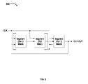
- FIG. 4 is a block diagram showing an exemplary frequency divider architecture having dynamic and static divider sections in accordance with embodiments of the present invention.
- FIG. 5 is a block diagram showing an exemplary RF divider circuit in accordance with embodiments of the present invention.
- FIG. 6 is a block diagram showing an exemplary dynamic divider arrangement in accordance with embodiments of the present invention.
- FIG. 7 is a schematic diagram showing an exemplary dynamic divider circuit designed with thin film transistors (TFTs) in accordance with embodiments of the present invention.
- FIG. 8 is a block diagram showing an exemplary static divider arrangement in accordance with embodiments of the present invention.
- FIG. 9 is a schematic diagram showing an exemplary static divider circuit designed with TFTs in accordance with embodiments of the present invention.
- FIG. 10 is a flow diagram showing an exemplary method of implementing or designing a divider circuit using TFTs, in accordance with embodiments of the present invention.
- FIG. 11 is a flow diagram showing an exemplary method of dividing the frequency of a periodic signal using a divider circuit including TFTs, in accordance with embodiments of the present invention.
- these quantities take the form of electrical, magnetic, optical, or quantum signals capable of being stored, transferred, combined, compared, and otherwise manipulated in a computer or data processing system. It has proven convenient at times, principally for reasons of common usage, to refer to these signals as bits, waves, waveforms, streams, values, symbols, characters, terms, numbers, or the like, and to their representations in computer programs or software as code (which may be object code, source code or binary code).
- the terms refer to actions and processes of the processing devices that manipulate or transform physical quantities within the component(s) of a circuit, system or architecture (e.g., registers, memories, other such information storage, transmission or display devices, etc.) into other data similarly represented as physical quantities within other components of the same or a different system or architecture.
- a circuit, system or architecture e.g., registers, memories, other such information storage, transmission or display devices, etc.
- the terms “wire,” “wiring,” “line,” “signal,” “conductor” and “bus” refer to any known structure, construction, arrangement, technique, method and/or process for physically transferring a signal from one point in a circuit to another.
- the terms “known,” “fixed,” “given,” “certain” and “predetermined” generally refer to a value, quantity, parameter, constraint, condition, state, process, procedure, method, practice, or combination thereof that is, in theory, variable, but is typically set in advance and not varied thereafter when in use.
- clock time
- timing timing
- rate rate
- period period
- frequency frequency
- data data stream
- bits bits
- bit string bits
- waveform waveform
- information may be used interchangeably, as may the terms “connected to,” “coupled with,” “coupled to,” and “in communication with” (which may refer to direct or indirect connections, couplings, or communications), but these terms are generally given their art-recognized meanings herein.
- a “tag” may be a single device or a sheet and/or spool of attached structures suitable for wireless, display, sensor, flexible, high frequency (HF), very high frequency (VHF), ultrahigh frequency (UHF), radio frequency (RF) and/or RF identification (RFID) applications.
- HF high frequency
- VHF very high frequency
- UHF ultrahigh frequency
- RFID radio frequency
- the term “deposit” (and grammatical variations thereof) is intended to encompass all forms of deposition, including blanket deposition (e.g., CVD and PVD), coating, and printing.
- printing may comprise inkjetting, gravure printing, offset printing, flexographic printing, screen printing, slit extruding, microspotting and/or selectively pen-coating an ink formulation onto the substrate.
- coating may comprise spin-coating, spray-coating, slit coating, extrusion coating, meniscus coating, dip coating, and/or pen-coating the ink formulation onto the substrate.
- coating refers to a process where the ink or other material is deposited on substantially the entire substrate, whereas printing generally refers to a process where the ink or other material is deposited in a predetermined pattern in certain areas of the substrate.
- the substrate generally comprises a mechanical support structure, which may be electrically inert or active, and which may include one or more predetermined physical, electrical and/or optical properties.
- Suitable electrically inert or inactive substrates may comprise a glass or other ceramic plate, disc, sheet or slip (e.g., comprising display-type glass, quartz, etc.), a dielectric and/or a plastic sheet or disc (e.g., a transparent plastic such a polycarbonate sheet, etc.), laminated variations thereof, etc.
- suitable electrically conductive substrates may comprise a semiconductor wafer or disc (e.g., a silicon wafer), a metal disc, sheet or foil (e.g., a metal film, metal sheet, and/or metal foil), etc.
- any of the above-mentioned substrates may further include one or more buffer, passivation, planarization, barrier, mechanical support and/or insulating layers thereon.
- the buffer, planarization, barrier and/or insulating layer may comprise a polyimide or other polymer layer or sheet, silicon dioxide and/or aluminum oxide, an amorphous alloy or metal compound (such as TiN), etc.
- Embodiments of the present invention can advantageously provide an approach that overcomes the issues and/or problems associated with the leakage and speed characteristics of TFTs in implementing a frequency divider suitable for use in wide variety of circuits and systems. Further, embodiments of the present invention can advantageously be designed, manufactured and/or otherwise implemented using printing technology. The invention, in its various aspects, will be explained in greater detail below with regard to exemplary embodiments.
- Various embodiments of the present invention provide a frequency divider architecture and frequency divider circuitry that can be implemented using TFTs and/or manufactured using additive technologies (such as printing).
- a frequency divider includes a dynamic divider section and a static divider section. All such circuit portions can be printable in order to reduce overall system and/or manufacturing costs. Further, “on-the-fly” customization of individual tags, circuits, and devices, including the frequency dividers or sections/stages therein, during the manufacturing process can also be accommodated.
- a TFT is a kind of field-effect transistor (FET) that may be made by depositing and patterning a series of thin films on or over a supporting substrate, including a semiconductor active layer (including a channel and source and drain terminals), one or more dielectric layers, a gate layer, and one or more electrical contact layers to the source and drain terminals (and, in some cases, to the gate).
- the TFT includes metal electrodes to the electrical contact layers (and, in some cases, to the gate).
- the semiconductor layer can include amorphous silicon, monocrystalline silicon, or polycrystalline silicon.
- TFTs include compound semiconductors (e.g., metal chalcogenides, including late transition metal chalcogenides such as cadmium selenide, and semiconducting alloys thereof), and metal oxides (e.g., zinc oxide and semiconducting alloys of metal oxides, such as zinc indium gallium oxide).
- compound semiconductors e.g., metal chalcogenides, including late transition metal chalcogenides such as cadmium selenide, and semiconducting alloys thereof
- metal oxides e.g., zinc oxide and semiconducting alloys of metal oxides, such as zinc indium gallium oxide
- TFTs can also be made using organic materials (Organic TFT or OTFT).
- Frequency dividers can generally be implemented as “static,” “semi-static,” or “dynamic” types of circuits.
- a static divider circuit uses a true bi-stable circuit (which in some applications may function as a kind of memory element), whereas a dynamic divider circuit uses capacitance (e.g., parasitic capacitance or stored capacitance) to determine a value of a signal at various nodes within the circuit.
- capacitance e.g., parasitic capacitance or stored capacitance
- TFTs may limit usability in dynamic dividers operating at relatively low frequencies because charge for storage may be lost through leakage prior to switching.
- an optimized partitioning combines dynamic and static (or semi-static) frequency divider stages using TFTs to overcome associated drawbacks of each frequency divider type.
- FIG. 3 shows a block diagram 300 of an exemplary RFID tag architecture suitable for use in accordance with embodiments of the present invention. Similar architectures may be suitable for HF, VHF and UHF tags or devices.
- An electromagnetic field can be induced on an antenna attached at terminals Coil 1 and Coil 2 and across capacitor CR.
- the AC voltage across the coil can be rectified by full wave rectifier 302 to form a DC power supply across terminals VDD/VSS and supply capacitance, CS.
- the DC power supply is provided to the remaining circuit blocks in the tag 300 .
- RF-to-DC conversion can be achieved using one or more rectifiers (e.g., full wave rectifier 302 , or alternatively, a bridge-type rectifier or other clamp circuit) or, for UHF, VHF and HF applications, thin film diode structures formed from a silicon ink (e.g., an ink containing a source of elemental silicon, such as silicon nanoparticles and/or a hydrosilane compound containing a chain of at least 5 covalently-bound silicon atoms).
- a silicon ink e.g., an ink containing a source of elemental silicon, such as silicon nanoparticles and/or a hydrosilane compound containing a chain of at least 5 covalently-bound silicon atoms.
- diode-connected TFTs i.e., a TFT having its gate connected to a source or drain of the same transistor.
- Thin film devices having one or more layers made from a silicon ink with mobilities of >10 cm 2 /vs in the diode transport direction, doping in the range of 10 17 -10 20 cm ⁇ 3 , and contact resistances on the order of 10 ⁇ 5 ohm-cm 2 provide rectification in the GHz regime, of sufficient efficiency to power an RFID circuit.
- GHz rectification to DC and ⁇ 2 nsec gate delays have been demonstrated experimentally for a vertical thin film diode structure and a self-aligned TFT structure, respectively, having a semiconductor layer made from a silicon ink.
- Demodulation of clock and data signals, encoded as a subcarrier or subcarrier modulation on the carrier RF signal, can be achieved with simple voltage detectors based on thin film diodes, or diode-connected TFTs, as described herein. Optimal signal extraction may benefit from filtering and/or tuned capacitors.
- logic to perform control and readout (I/O) functions can be realized with printed TFTs in CMOS or NMOS technologies, using materials as described herein.
- CMOS has a significant advantage over NMOS in terms of power efficiency, but may use additional process steps or additional process complexity (e.g., multiple dopant inks) compared to NMOS technology.
- modulation is typically done by load modulation with a shunt transistor in parallel with a resonant capacitor.
- a modulator TFT made from a silane ink formulation in enhancement mode
- the LC coil that forms the tag's antenna is shorted. This dramatically reduces the Q of the circuit and the coupling to the reader coil.
- the TFT is switched sufficiently ‘off,’ the Q of the LC coil is restored. In this way, a modulation signal can be passed from the tag to the reader.
- Similar effects also vary the scattering cross-section of the antenna and modulate the backscatter signal to the reader.
- An antenna for RFID 300 may be implemented using a resonant LC circuit for use, e.g., at about 13.56 MHz. Alternatively, the antenna may be implemented using a dipole or similar such antenna for 900 MHz or 2.4 GHz operation. Generally, the antenna may be used to provide power for operation of the tag circuitry, and to provide information from the tag to the reader or interrogator. Power can be extracted at full wave rectifier 302 by rectifying the RF signal collected by the antenna, and storing the resultant charge in a storage capacitor (e.g., CR).
- a storage capacitor e.g., CR
- a clock signal (e.g., “logic clock”) can be generated so as to synchronously operate associated circuitry (e.g., sequencer 306 , a counter circuit, etc.).
- This clock signal may be generated by dividing down (e.g., via frequency divider circuitry) the incident RF signal received by the antenna or by dividing a demodulated clock signal from the received RF signal.
- This clock signal may be used to drive a counter to begin counting from a reset state when enabled. As the counter value increases, the counter output can be used to sequentially select specific bits in memory array 308 to provide serial data out to data encoder 310 .
- Bits provided from memory array 308 in tag or device 300 may be passed to an output stage (e.g., via data encoder 310 ) for information (e.g., in the form of a bit string) transfer back to a reader or interrogator.
- the information transfer can be accomplished by modulation (e.g., via data modulator 312 ) of the tag impedance.
- modulation e.g., via data modulator 312
- other common modulation schemes such as amplitude and/or frequency shift keying may also be used in certain embodiments.
- a frequency divider circuit includes (i) a dynamic section configured to receive an input signal that has a first frequency, and to output an intermediate signal that has a second frequency lower than the first frequency; and (ii) a static section configured to receive the intermediate signal, and output a signal having a third frequency that is lower than the second frequency.
- the dynamic and/or static divider sections can include TFT devices.
- FIG. 4 shows a block diagram 400 of an exemplary frequency divider with dynamic and static divider sections, in accordance with embodiments of the present invention.
- Dynamic section 402 receives an input clock (CLK), and provides an intermediate signal 406 .
- Intermediate signal 406 is generally a frequency divided version of the input clock.
- Static section 404 receives intermediate signal 406 , and provides a frequency divided clock (CLK/N), which is a frequency divided version of the intermediate signal 406 , and a further frequency divided version of the input clock.
- CLK/N frequency divided clock
- the input clock CLK is generally from clock extractor and/or demodulator circuitry on the tag or device.
- the static circuitry may employ bi-stable memory elements, while the dynamic circuitry includes parasitic and/or other capacitances that are subject to leakage.
- TFT-based dynamic dividers At relatively high frequencies, charge loss due to leakage in TFT-based dynamic dividers may not be a significant concern because the dividers can switch before charge is lost. However, such dynamic dividers may not be suitable for operation at lower frequencies because of this leakage characteristic. At relatively low frequencies, TFT-based static (or semi-static) dividers can provide good stability, while maintaining reasonable operation. However, these static and semi-static dividers may not be suitable for use at high frequencies due to relatively poor mobility in the TFTs, possibly preventing correct switching at relatively high frequencies.
- a frequency divider chain can be implemented using a TFT-based dynamic divider (or series of divider stages) at high frequencies (e.g., above a predetermined threshold frequency), while using a TFT-based static or semi-static divider (or series of divider stages) at low frequencies (e.g., below a predetermined threshold frequency).
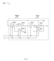
- FIG. 5 shows a block diagram 500 of an exemplary divider circuit in accordance with an embodiment of the present invention.
- a partitioning scheme is used to reduce or avoid the disadvantageous effects of the leakage and speed characteristics of TFTs.
- the divider circuit 500 is used to divide an incoming RF signal 506 having a frequency of about 13.56 MHz to produce an output signal 520 having a frequency of about 106 kHz.
- dynamic divider section 402 divides the input signal 506 from about 13.56 MHz down to about 1.6 MHz (the characteristic frequency of intermediate signal 406 ), and in a second part, static divider section 404 divides the intermediate signal 406 down to about 106 kHz at (the characteristic frequency of the output signal 520 ).
- Dynamic section 402 divides the input signal 506 using a plurality of serial stages, including first dynamic divider circuit 502 - 0 , second dynamic divider circuit 502 - 1 , and dynamic divider circuit 502 - 2 .
- First dynamic divider circuit 502 - 0 produces a divided clock signal 508 having a frequency of about 6.7 MHz.
- Second dynamic divider circuit 502 - 1 produces a divided clock signal 510 having a frequency of about 3.3 MHz.
- Third dynamic divider circuit 502 - 2 produces a divided clock signal (intermediate signal 406 ) having a frequency of about 1.6 MHz.
- any dynamic divider stage may have any integer “divide-by” ratio (e.g., 3, 4, 5, 6, 8, etc.) and, optionally, any integer multiplier ratio (e.g., 3, 4, 5, 6, 8, etc.) implementable using transistor logic, as long as the intermediate signal 406 has a frequency less than that of the input signal 506 .
- the second frequency is the first frequency multiplied by p/q, where p is an integer, q is an integer greater than or equal to 2, and p/q ⁇ 1.
- the intermediate signal 406 has a frequency above a predetermined threshold frequency (e.g., a maximum frequency at which static or semi-static divider circuits made using particular TFTs can operate reliably).
- Static section 404 divides the intermediate signal 406 using a plurality of serial stages, including first static divider circuit 504 - 0 , second static divider circuit 504 - 1 , third static divider circuit 504 - 2 , and fourth static divider circuit 504 - 3 .
- First static divider circuit 504 - 0 produces a divided clock signal 514 having a frequency of about 847 kHz.
- Second static divider circuit 504 - 1 produces a divided clock signal 516 having a frequency of about 423 kHz.
- Third static divider circuit 504 - 2 produces a divided clock signal 518 having a frequency of about 212 kHz.
- Fourth static divider circuit 504 - 3 produces a divided clock signal (output signal 520 ) having a frequency of about 106 kHz.
- Each of the first, second, third, and fourth static divider circuits 504 - 0 , 504 - 1 , 504 - 2 and 504 - 3 may be static or semi-static.
- any static divider stage may have any integer “divide-by” ratio (e.g., 3, 4, 5, 6, 8, etc.) and, optionally, any integer multiplier ratio (e.g., 3, 4, 5, 6, 8, etc.) implementable using transistor logic, as long as the output signal 520 has a frequency less than that of the intermediate signal 406 .
- the third frequency is the second frequency multiplied by p′/q′, where p′ is an integer, q′ is an integer greater than or equal to 2, and p′/q′ ⁇ 1.
- the output signal 520 has a frequency below the predetermined threshold frequency as described in the preceding paragraph (which may also be, e.g., a minimum frequency below which dynamic divider circuits made using particular TFTs may not operate reliably).
- any suitable number of dynamic stages 502 e.g., 1, 2, 4, 5, etc.
- static stages 504 e.g., 1, 2, 3, 5, 6, 7, etc.
- different frequency divider stages can be individually enabled or disabled via any suitable form of user programming (e.g., metal layer or fuse programming, software control, etc.) or selection during the manufacturing process.
- printing technology can be used to control the enabling/disabling of such frequency divider stages during the manufacturing process.
- FIG. 6 shows a block diagram 600 of an exemplary dynamic divider arrangement in accordance with embodiments of the present invention.
- the dynamic divider stages can be implemented using a variety of methods.
- arrangement 600 can be used in implementation of a dynamic divider stage 502 , as shown in FIG. 5 .
- a number of TFT-based dynamic divider segments e.g., segments 602 - 0 , 602 - 1 , . . . 602 -N
- cascaded outputs and feedback e.g., CLK OUT as an input to first segment 602 - 0
- the number of such dynamic divider segments in one dynamic divider stage can be 2p+1, where p is a positive integer.
- any suitable dynamic frequency divider arrangement or circuitry can be used in particular embodiments.
- FIG. 7 shows a schematic diagram 700 of an exemplary dynamic divider circuit with TFTs in accordance with embodiments of the present invention.
- three TFT-based dynamic divider segments e.g., segments 602 - 0 , 602 - 1 and 602 - 2 of FIG. 6 .
- the input signal CLK is received at transistors M 0 - 2 , M 1 - 1 , M 1 - 3 , and M 2 - 2 .
- a first TFT-based dynamic divider segment 602 - 0 includes transistors M 0 - 1 , M 0 - 2 and M 0 - 3 , and provides signal 702 to the gate of transistor M 1 - 2 in the second segment 602 - 1 .
- the second TFT-based segment 602 - 1 includes transistors M 1 - 1 , M 1 - 2 , and M 1 - 3 , and provides signal 704 to the gates of transistor M 2 - 1 and M 2 - 3 in the third segment 602 - 2 .
- the third TFT-based segment 602 - 2 includes transistors M 2 - 1 , M 2 - 2 , and M 2 - 3 , and provides frequency divided signal “Div 2 ,” which can be fed back into transistors M 0 - 1 and M 0 - 3 in the first segment 602 - 0 .
- each segment of the dynamic frequency divider stage 700 comprises a p-channel thin film transistor, an n-channel thin film transistor, and a third thin film transistor coupled between the p-channel and n-channel thin film transistors.
- each dynamic frequency divider stage 700 in the frequency divider circuit may receive the output signal (e.g., Div 2 ) of the dynamic frequency divider stage 700 as a feedback signal from a last segment (e.g., 602 - 2 ) of the dynamic frequency divider stage 700 , and each successive segment (e.g., 602 - 1 , 602 - 2 ) of the dynamic frequency divider stage receives a segment output signal from a preceding segment (e.g., 602 - 0 , 602 - 1 , respectively).
- a preceding segment e.g., 602 - 0 , 602 - 1 , respectively.
- each segment 602 - n may receive a plurality of input signals, including the input signal CLK of the dynamic frequency divider stage 700 and an output signal (e.g., 702 , 704 , Div 2 ) from another segment within the stage 700 .
- an output signal e.g., 702 , 704 , Div 2
- a frequency of the incoming signal CLK can be divided in half at output Div 2 , which is generally the output of the dynamic divider stage 502 .
- output Div 2 which is generally the output of the dynamic divider stage 502 .
- any number of segments e.g., 5, 7, 9, etc., or any other odd number greater than 1 can be employed.
- TFT sizing and other design considerations can be used to adjust circuit performance (e.g., implement a desired or predetermined operational frequency range or frequency division factor).
- FIG. 8 shows a block diagram 800 of an exemplary static divider arrangement in accordance with embodiments of the present invention.
- the static divider stages e.g., static stages 504 - 0 , 504 - 1 , 504 - 2 and 504 - 3 of FIG. 5
- a master-slave arrangement can be used to provide a static-type signal frequency divider circuit.
- master stage 802 provides a signal 804 to slave stage 806 , which provides frequency divided output signal DIV 2 .
- each of the master stage 802 and the slave stage 806 comprise a flip-flop.
- each static frequency divider stage 800 may comprise a first flip-flop 802 configured to receive an input signal CLK from the preceding static frequency divider stage and a feedback signal corresponding to the static frequency divider stage output signal DIV 2 , and a second flip-flop configured to receive the input signal CLK from the preceding static frequency divider stage and provide the static frequency divider stage output signal DIV 2 .
- FIG. 9 shows a block schematic diagram 900 of an exemplary static divider circuit including TFTs, in accordance with embodiments of the present invention.
- Master stage flip-flop 802 includes pass-gate 902 - 0 , inverters 904 - 0 and 906 - 0 , and pass-gate 908 - 0 .
- the static memory element for the flip-flop is formed by the inverter structure (together with feedback/cross-coupling loop 804 ).
- Signal 804 is also output from master stage flip-flop 802 to slave stage flip-flop 806 , which includes pass-gate 902 - 1 , inverters 904 - 1 and 906 - 1 , and pass-gate 908 - 1 .
- Other types of flip-flops, logic gates, or other similar circuit arrangements can also be used in particular embodiments.
- a method of implementing or designing a divider circuit includes (i) determining a divider ratio for a given periodic signal having a characteristic frequency; (ii) determining a degradation tolerance of signal quality based on the characteristics of thin film transistors in the divider circuit; (iii) calculating a threshold frequency at which the periodic signal, divided by a divider comprising the thin film transistors, degrades beyond the degradation tolerance; and (iv) designing a dynamic divider circuit to divide the periodic signal above the threshold frequency and a corresponding static divider circuit to divide the periodic signal below the threshold frequency.
- FIG. 10 shows a flow diagram 1000 of an exemplary method of implementing a divider circuit using TFTs, in accordance with embodiments of the present invention.
- the flow can begin ( 1002 ), and a divider ratio can be determined for a given periodic signal that has a characteristic frequency ( 1004 ).
- the known frequency of the input clock or other periodic signal is divided by the desired output frequency, and the fraction or integer-to-integer ratio closest to the calculated number is used as the divider ratio.
- the nearest integer ratio that is a factor of 2, 3 and/or 5 (e.g., 16, 20, 24, 32, 40, 64, 128, etc.) closest to (and optionally, greater or less than) the calculated number may be selected.
- the degradation tolerance of signal quality is determined based on the characteristics of the TFTs ( 1006 ).
- the signal for which signal quality is determined may be the periodic signal that is input into the frequency divider (e.g., the logic clock of FIG. 3 or input clock CLK of FIG. 6 ), or it may be a standard signal of the type used to test signal degradation (e.g., a signal that can be used to determine hysteresis properties).
- the degradation tolerance may be determined based on a plurality of characteristics of the thin film transistors, such as leakage (e.g., under predetermined conditions, such as a applying a maximum voltage differential across the source and drain when the transistor is off), mobility, and/or speed.
- a threshold frequency can be calculated at which the periodic signal, divided by a divider using the TFTs, degrades beyond the degradation tolerance ( 1008 ).
- a suitable range for operation of dynamic dividers designed using printed TFTs made from a silane ink, doped by diffusion of dopant from a spin-on dopant can be from about 13.56 MHz down to about 1.6 MHz, while a suitable range for static dividers can be from about 1.6 MHz down to about 106 kHz.
- the threshold frequency may be from about 1 MHz to about 1.5 MHz.
- a dynamic divider circuit can then be designed to divide the periodic signal above the threshold frequency and a corresponding static divider circuit to divide the periodic signal to a value below the threshold frequency ( 1010 ), completing the flow ( 1012 ).
- a periodic signal may be divided by (i) dividing the periodic signal with one or more dynamic frequency divider stages, thereby creating an intermediate signal having a frequency less than that of the periodic signal; and (ii) dividing the intermediate signal with one or more static frequency divider stages to create an output signal having a frequency less than that of the intermediate signal.
- both the dynamic frequency divider stage(s) and the static frequency divider stages include TFTs.
- FIG. 11 shows a flow diagram 1100 of an exemplary method of dividing a frequency of a periodic signal using divider circuits comprising TFTs, in accordance with embodiments of the present invention.
- the flow begins ( 1102 ), and a periodic signal can be divided using one or more dynamic frequency divider stages as described above to create an intermediate signal ( 1104 ).
- the intermediate signal is generally periodic, and it has a frequency less than the frequency of the input periodic signal.
- three dynamic divider stages 502 can be used. While relatively simple embodiments may divide the periodic signal by an integer ratio, the periodic signal may be divided by any fractional ratio less than one, as long as frequency of the produced intermediate signal is about the threshold frequency (as described herein).
- the intermediate periodic signal can then be divided using one or more static frequency divider stages, to create an output signal having a third frequency less than the second frequency ( 1106 ), thereby completing the flow ( 1108 ).
- four static divider stages 504 can be used.
- the dynamic frequency divider stages (see, e.g., FIG. 7 ) and/or the static frequency divider stages (see, e.g., FIG. 9 ) generally include TFTs.
- While the above examples include particular implementations of frequency divider and other tag circuitry, one skilled in the art will recognize that other technologies may also be used. For example, transistor types other than TFT transistors can be used in certain embodiments. Further, one skilled in the art will recognize that other forms of signaling and/or control (e.g., current-based signaling, differential signaling, etc.) may also be used in accordance with various embodiments.
Landscapes
- Engineering & Computer Science (AREA)
- Computer Networks & Wireless Communication (AREA)
- Computer Hardware Design (AREA)
- Microelectronics & Electronic Packaging (AREA)
- Physics & Mathematics (AREA)
- General Physics & Mathematics (AREA)
- Theoretical Computer Science (AREA)
- Thin Film Transistor (AREA)
Abstract
Description
| Application No. | Filing Date | Attorney Docket No. | ||
| 10/616,147 | Jul. 8, 2003 | KOV-004 | ||
| 10/949,013 | Sep. 24, 2004 | IDR0302 | ||
| 10/950,373 | Sep. 24, 2004 | IDR0301 | ||
| 10/956,714 | Oct. 1, 2004 | IDR0303 | ||
| 11/867,587 | Oct. 4, 2007 | IDR0884 | ||
| 11/452,108 | Jun. 12, 2006 | IDR0502 | ||
| 11/805,620 | May 23, 2007 | IDR0712 | ||
| 11/888,942 | Aug. 3, 2007 | IDR0743 | ||
| 11/888,949 | Aug. 3, 2007 | IDR0742 | ||
| 11/818,078 | Jun. 12, 2007 | IDR0813 | ||
| 11/842,884 | Aug. 21, 2007 | IDR0982 | ||
| 10/789,274 | Feb. 27, 2004 | IDR0080 | ||
| 11/243,460 | Oct. 3, 2005 | IDR0272 | ||
| 11/940,161 | Nov. 14, 2007 | IDR0852 | ||
| 11/203,563 | Aug. 11, 2005 | IDR0213 | ||
| 11/870,775 | Oct. 11, 2007 | IDR1006 | ||
| 11/521,924 | Sep. 15, 2006 | IDR0692 | ||
| 12/114,741 | May 2, 2008 | IDR1102 | ||
| 12/109,338 | Apr. 24, 2008 | IDR1322 | ||
| 12/131,002 | May 30, 2008 | IDR1263 | ||
Claims (51)
Priority Applications (1)
| Application Number | Priority Date | Filing Date | Title |
|---|---|---|---|
| US12/537,724 US8085068B1 (en) | 2008-08-08 | 2009-08-07 | Combined static and dynamic frequency divider chains using thin film transistors |
Applications Claiming Priority (2)
| Application Number | Priority Date | Filing Date | Title |
|---|---|---|---|
| US8716708P | 2008-08-08 | 2008-08-08 | |
| US12/537,724 US8085068B1 (en) | 2008-08-08 | 2009-08-07 | Combined static and dynamic frequency divider chains using thin film transistors |
Publications (1)
| Publication Number | Publication Date |
|---|---|
| US8085068B1 true US8085068B1 (en) | 2011-12-27 |
Family
ID=45349840
Family Applications (1)
| Application Number | Title | Priority Date | Filing Date |
|---|---|---|---|
| US12/537,724 Expired - Fee Related US8085068B1 (en) | 2008-08-08 | 2009-08-07 | Combined static and dynamic frequency divider chains using thin film transistors |
Country Status (1)
| Country | Link |
|---|---|
| US (1) | US8085068B1 (en) |
Cited By (2)
| Publication number | Priority date | Publication date | Assignee | Title |
|---|---|---|---|---|
| WO2021050345A1 (en) * | 2019-09-13 | 2021-03-18 | The Regents Of The University Of California | Spectrum-compressing receiver and reception method for non-contiguous carrier aggregation |
| US11321599B2 (en) * | 2019-04-30 | 2022-05-03 | Em Microelectronic-Marin Sa | Dual frequency HF-UHF identification integrated circuit |
Citations (1)
| Publication number | Priority date | Publication date | Assignee | Title |
|---|---|---|---|---|
| US20060208775A1 (en) * | 2005-03-16 | 2006-09-21 | Mitsubishi Denki Kabushiki Kaisha | Frequency dividing circuit, power supply circuit and display device |
-
2009
- 2009-08-07 US US12/537,724 patent/US8085068B1/en not_active Expired - Fee Related
Patent Citations (1)
| Publication number | Priority date | Publication date | Assignee | Title |
|---|---|---|---|---|
| US20060208775A1 (en) * | 2005-03-16 | 2006-09-21 | Mitsubishi Denki Kabushiki Kaisha | Frequency dividing circuit, power supply circuit and display device |
Cited By (3)
| Publication number | Priority date | Publication date | Assignee | Title |
|---|---|---|---|---|
| US11321599B2 (en) * | 2019-04-30 | 2022-05-03 | Em Microelectronic-Marin Sa | Dual frequency HF-UHF identification integrated circuit |
| WO2021050345A1 (en) * | 2019-09-13 | 2021-03-18 | The Regents Of The University Of California | Spectrum-compressing receiver and reception method for non-contiguous carrier aggregation |
| US12267094B2 (en) | 2019-09-13 | 2025-04-01 | The Regents Of The University Of California | Spectrum-compressing receiver and reception method for non-contiguous carrier aggregation |
Similar Documents
| Publication | Publication Date | Title |
|---|---|---|
| US20180225559A1 (en) | Printed Radio Frequency Identification (RFID) Tag Using Tags-Talk-First (TTF) Protocol | |
| Myny et al. | Plastic circuits and tags for 13.56 MHz radio-frequency communication | |
| KR101389119B1 (en) | Oscillator circuit and semiconductor device including the same | |
| US7750792B2 (en) | Multi-mode tags and methods of making and using the same | |
| US8095104B2 (en) | Semiconductor device and electronic device having the same | |
| US8243863B2 (en) | Semiconductor device | |
| Myny et al. | Flexible thin-film NFC tags | |
| WO2008078661A1 (en) | Semiconductor device | |
| JP5222545B2 (en) | Transmission / reception circuit and semiconductor device including the transmission / reception circuit | |
| US8085068B1 (en) | Combined static and dynamic frequency divider chains using thin film transistors | |
| US7786818B2 (en) | Electronic component comprising a modulator | |
| US7746143B2 (en) | Clock generating circuit and semiconductor device provided with clock generating circuit | |
| JP5204998B2 (en) | Semiconductor device | |
| TW201031153A (en) | Modulation circuit and semiconductor device including the same | |
| US8022410B2 (en) | Thin film transistors | |
| US7978787B2 (en) | Semiconductor device | |
| Cho et al. | Oxide thin film transistor circuits for transparent RFID applications | |
| Chang et al. | Fully-additive printed RFID on a plastic film | |
| Clemens et al. | Printed RFID and Smart Objects for new high volume applications | |
| Subramanian et al. | Radiofrequency identification (RFID) manufacturing: A case study | |
| Lugli et al. | RFID: Ideas for Future Development | |
| Myny et al. | Towards EPC compatible plastic RFID tags | |
| Dehaene et al. | Kris Myny1, 2, 3, Soeren Steudel1, Peter Vicca1, Monique J. Beenhakkers4, Nick AJM van Aerle4, Gerwin H. Gelinck5, Jan Genoe1, 2 |
Legal Events
| Date | Code | Title | Description |
|---|---|---|---|
| AS | Assignment |
Owner name: KOVIO, INC., CALIFORNIA Free format text: ASSIGNMENT OF ASSIGNORS INTEREST;ASSIGNOR:SUBRAMANIAN, VIVEK;REEL/FRAME:023087/0726 Effective date: 20090806 |
|
| AS | Assignment |
Owner name: THIN FILM ELECTRONICS ASA, NORWAY Free format text: ASSIGNMENT OF ASSIGNORS INTEREST;ASSIGNOR:KOVIO, INC.;REEL/FRAME:032126/0931 Effective date: 20140122 |
|
| REMI | Maintenance fee reminder mailed | ||
| LAPS | Lapse for failure to pay maintenance fees | ||
| STCH | Information on status: patent discontinuation |
Free format text: PATENT EXPIRED DUE TO NONPAYMENT OF MAINTENANCE FEES UNDER 37 CFR 1.362 |
|
| STCH | Information on status: patent discontinuation |
Free format text: PATENT EXPIRED DUE TO NONPAYMENT OF MAINTENANCE FEES UNDER 37 CFR 1.362 |
|
| FP | Lapsed due to failure to pay maintenance fee |
Effective date: 20151227 |
|
| AS | Assignment |
Owner name: ENSURGE MICROPOWER ASA, CALIFORNIA Free format text: CHANGE OF NAME;ASSIGNOR:THIN FILM ELECTRONICS ASA;REEL/FRAME:061298/0249 Effective date: 20220819 |