US8079521B2 - Fractional down-sampling in imaging barcode scanners - Google Patents
Fractional down-sampling in imaging barcode scanners Download PDFInfo
- Publication number
- US8079521B2 US8079521B2 US12/425,640 US42564009A US8079521B2 US 8079521 B2 US8079521 B2 US 8079521B2 US 42564009 A US42564009 A US 42564009A US 8079521 B2 US8079521 B2 US 8079521B2
- Authority
- US
- United States
- Prior art keywords
- pixels
- pixel
- center
- row
- pixel data
- Prior art date
- Legal status (The legal status is an assumption and is not a legal conclusion. Google has not performed a legal analysis and makes no representation as to the accuracy of the status listed.)
- Active, expires
Links
Images


Classifications
-
- G—PHYSICS
- G06—COMPUTING; CALCULATING OR COUNTING
- G06K—GRAPHICAL DATA READING; PRESENTATION OF DATA; RECORD CARRIERS; HANDLING RECORD CARRIERS
- G06K7/00—Methods or arrangements for sensing record carriers, e.g. for reading patterns
- G06K7/10—Methods or arrangements for sensing record carriers, e.g. for reading patterns by electromagnetic radiation, e.g. optical sensing; by corpuscular radiation
- G06K7/10544—Methods or arrangements for sensing record carriers, e.g. for reading patterns by electromagnetic radiation, e.g. optical sensing; by corpuscular radiation by scanning of the records by radiation in the optical part of the electromagnetic spectrum
- G06K7/10712—Fixed beam scanning
- G06K7/10722—Photodetector array or CCD scanning
-
- G—PHYSICS
- G06—COMPUTING; CALCULATING OR COUNTING
- G06K—GRAPHICAL DATA READING; PRESENTATION OF DATA; RECORD CARRIERS; HANDLING RECORD CARRIERS
- G06K7/00—Methods or arrangements for sensing record carriers, e.g. for reading patterns
- G06K7/10—Methods or arrangements for sensing record carriers, e.g. for reading patterns by electromagnetic radiation, e.g. optical sensing; by corpuscular radiation
- G06K7/10544—Methods or arrangements for sensing record carriers, e.g. for reading patterns by electromagnetic radiation, e.g. optical sensing; by corpuscular radiation by scanning of the records by radiation in the optical part of the electromagnetic spectrum
- G06K7/10821—Methods or arrangements for sensing record carriers, e.g. for reading patterns by electromagnetic radiation, e.g. optical sensing; by corpuscular radiation by scanning of the records by radiation in the optical part of the electromagnetic spectrum further details of bar or optical code scanning devices
- G06K7/10851—Circuits for pulse shaping, amplifying, eliminating noise signals, checking the function of the sensing device
Definitions
- the present disclosure relates generally to imaging readers for reading bar code symbols.
- Solid-state imaging systems or imaging readers have been used, in both handheld and hands-free modes of operation, to electro-optically read targets, such as one-dimensional bar code symbols, particularly of the Universal Product Code (UPC) type, each having a linear row of bars and spaces spaced apart along a scan direction, as well as two-dimensional symbols, such as Code 49, which introduced the concept of vertically stacking a plurality of rows of bar and space patterns in a single symbol, as described in U.S. Pat. No. 4,794,239.
- UPC Universal Product Code
- Code 49 Two-dimensional symbols
- PDF417 Another two-dimensional code structure for increasing the amount of data that can be represented or stored on a given amount of surface area is known as PDF417 and is described in U.S. Pat. No. 5,304,786.
- the imaging reader includes an imaging module having a solid-state imager with a sensor array of photocells or light sensors, which correspond to image elements or pixels in a two-dimensional field of view of the imager, and an imaging lens assembly for capturing return light scattered and/or reflected from the symbol being imaged, and for projecting the return light onto the sensor array to initiate capture of an image of the symbol as pixel data.
- the imager may be a one- or two-dimensional charge coupled device (CCD) or a complementary metal oxide semiconductor (CMOS) device and includes associated circuits for producing and processing electrical signals corresponding to a one- or two-dimensional array of the pixel data over the field of view.
- CCD charge coupled device
- CMOS complementary metal oxide semiconductor
- the imager captures the return light under the control of a controller or programmed microprocessor that is operative for processing and decoding the electrical signals into data indicative of the symbol being imaged and read.
- the controller selectively energizes selected sensors and, in effect, maps or draws at least one virtual scan line across the symbol, in a manner analogous to a real scan line of a moving laser reader or laser scanner also operative for electro-optically reading such symbols.
- high resolution solid-state imagers are used.
- a solid-state imager can have a resolution of 1280 ⁇ 960 pixels or more.
- the solid-state imager may need to output images at a relatively frame rate of, for example, about 30-60 frames per second. The higher frame rate allows the imager to effectively capture images of fast-moving objects. Outputting high resolution images at high frame rated may impose large bandwidth requirement.
- the resolution of the output images can be reduced from the original images by a factor of 2 ⁇ 2. But reductions by factors of 2 or higher could pose more severe limitations than downstream image analysis software can handle. In certain applications, it is desirable to reduce the resolution of the output images from the original images by a fractional ratio, such as, by a factor of 3/2 ⁇ 3/2, as a compromise between higher resolution images and higher frame rates.
- the invention is directed to a method of improving the performance of an imaging reader.
- the method includes (1) illuminating a symbol by projecting illuminating light on the symbol from the imaging reader, (2) capturing return light form the symbol as pixel data over a two-dimensional field of view of a solid-state imager having a matrix of image sensors, (3) merging the number of pixels to generate reduced pixel data with a co-processor, (4) transmitting the reduced pixel data from the co-processor to a decoding circuit.
- the pixel data includes a section of a pixel matrix and the section has N rows and M columns of pixels.
- the reducing the number of pixels includes (a) dividing the M columns of pixels in the section of pixel matrix into multiple column groups, (b) for each given row of pixels in each column group, creating additional pixels in locations between the pre-existing pixel locations, whose values are obtained through calculations involving the values of those pixels in the given group, and (c) omitting some pixels.
- Implementations of the invention can include one or more of the following advantages.
- the resolution of the images output from the solid-state imager can be reduced by a fractional ratio.
- the bandwidth requirement to the decoder circuit can be reduced.
- FIG. 1 generally depict an imaging reader having a generally upright window and a gun-shaped housing supported by a base.
- FIG. 2 generally depict that a solid-state imager is mounted on a printed circuit board in the reader.
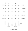
- FIG. 3A-3E shows a small section of pixels in an image and illustrate that the number of pixels of an image can be reduced by a fractional ratio in accordance with some embodiments.
- FIG. 4 shows a method 400 of reducing the number of pixels in a section a section of pixel matrix.
- Reference numeral 30 in FIG. 1 generally identifies an imaging reader having a generally upright window 26 and a gun-shaped housing 28 supported by a base 32 for supporting the imaging reader 30 on a countertop.
- the imaging reader 30 can thus be used in a hands-free mode as a stationary workstation in which products are swiped past, or presented to, the window 26 , or can be picked up off the countertop and held in an operator's hand and used in a handheld mode in which the reader is moved, and a trigger 34 is manually depressed to initiate imaging of indicia, especially one- or two-dimensional symbols, to be read at a distance from the window 26 .
- the base 32 can be omitted, and housings of other configurations can be employed.
- a cable, as illustrated in FIG. 1 connected to the base 32 can also be omitted, in which case, the reader 30 communicates with a remote host by a wireless link, and the reader is electrically powered by an on-board battery.
- an imager 24 is mounted on a printed circuit board 22 in the reader.
- the imager 24 is a solid-state device, for example, a CCD or a CMOS imager having a one-dimensional array of addressable image sensors or pixels arranged in a single, linear row, or a two-dimensional array of such sensors arranged in mutually orthogonal rows and columns, and operative for detecting return light captured by an imaging lens assembly 20 along an optical path or axis 46 through the window 26 .
- the return light is scattered and/or reflected from a target or symbol 38 as pixel data over a two-dimensional field of view 60 .
- the imaging lens assembly 20 is operative for adjustably focusing the return light onto the array of image sensors to enable the symbol 38 to be read.
- the symbol 38 is located anywhere in a working range of distances between a close-in working distance (WD 1 ) and a far-out working distance (WD 2 ).
- WD 1 is about four to six inches from the imager array 24
- WD 2 can be many feet from the window 26 , for example, around fifty feet away.
- An illuminating assembly is also mounted in the imaging reader and preferably includes an illuminator or illuminating light source 12 , e.g., a light emitting diode (LED) or a laser, and an illuminating lens assembly 10 to uniformly illuminate the symbol 38 with an illuminating light having an intensity level over an illumination time period.
- the light source 12 is preferably pulsed.
- An aiming assembly is also mounted in the imaging reader and preferably includes an aiming light source 18 , e.g., an LED or a laser, and an aiming lens assembly 16 for generating a visible aiming light pattern on the symbol 38 .
- the aiming pattern is useful to help the operator accurately aim the reader at the symbol 38 .
- the imager 24 , the illuminating light source 12 and the aiming light source 18 are operatively connected to a controller or programmed microprocessor 36 operative for controlling the operation of these components.
- the microprocessor 36 includes a decoder for processing the return light from the target symbols, and for decoding the captured target images.
- a memory 14 is accessible by the controller 36 for storing and retrieving data.
- the controller 36 sends a command signal to energize the aiming light source 18 prior to reading, and also pulses the illuminating light source 12 for the illumination time period, say 500 microseconds or less, and energizes and exposes the imager 24 to collect light, e.g., illumination light and/or ambient light, from the symbol during an exposure time period.
- a typical array needs about 16-33 milliseconds to transfer the date of the entire target image and operates at a frame rate of about 30-60 frames per second.
- FIG. 3A-3E shows that number of pixels of an image can be reduced by a fractional ratio.
- FIG. 3A-3E only a small section of pixels in an image is illustrated; that is, only pixels positioned within rows from 3m to 3m+7 and within columns from 3n to 3n+7 are illustrated.
- pixels positioned within rows from 3m to 3m+3 belong to a rows group m
- the pixels positioned within rows from 3m+3 to 3m+6 belong to a rows group (m+1).
- the rows group m and the rows group (m+1) each have four rows of pixels.
- the row 3(m+1) belongs to both of these two adjacent rows groups. That is, these two adjacent rows groups share one row of pixels in common.
- pixels positioned within columns from 3n to 3n+3 belong to a columns group n
- the pixels positioned within columns from 3n+3 to 3n+6 belong to a columns group (n+1).
- the columns group n and the columns group (n+1) each have four columns of pixels.
- the column 3(n+1) belongs to both of these two adjacent columns groups. That is, these two adjacent columns groups share one column of pixels in common.
- FIG. 3B shows that the two center columns in each column group can be merged into one column located at the center of the column group.
- the column 3n+1 and the column 3n+2 can be merged into one column labeled as 3[n+1 ⁇ 2] located at the center of the column group n; in the column group (n+1), the column 3(n+1)+1 and the column 3(n+1)+2 can be merged into one column labeled as 3[(n+1)+1 ⁇ 2] located at the center of the column group (n+1).
- FIG. 3C shows that the two center rows in each row group can be merged into one row located at the center of the row group as well.
- the row 3m+1 and the row 3m+2 can be merged into one row labeled as 3 [m+1 ⁇ 2] located at the center of the row group m; in the row group (m+1), the row 3(m+1)+1 and the row 3(m+1)+2 can be merged into one row labeled as 3[(m+1)+1 ⁇ 2] located at the center of the row group (m+1).
- FIG. 3D shows that that the number of rows and columns in an image can be reduced.
- FIG. 3D shows that only pixels in two types of columns are selected for output.
- the two types of columns are listed as follows: (1) the newly created column located at the center of each column group—e.g., column 3[n+1 ⁇ 2] or column 3[(n+1)+1 ⁇ 2]; (2) the common column shared by two adjacent columns—e.g., column 3n, column (n+1), or column (n+2).
- FIG. 3D only pixels in two types of rows are selected for output.
- the two types of rows are listed as follows: (1) the newly created row located at the center of each row group—e.g., row 3[m+1 ⁇ 2] or row 3[(m+1)+1 ⁇ 2]; (2) the common row shared by two adjacent rows—e.g., row 3m, row (m+1), or row (m+2).
- FIG. 3E shows that that the total number of pixels in an image is reduced by a fractional ratio and the reduction factor for the number of pixels is 3/2 ⁇ 3/2.
- the columns 3n, 3n+1, 3n+2 are reduced to columns 3n and 3[n+1 ⁇ 2]; the columns 3(n+1), 3(n+1)+1, 3(n+1)+2 are reduced to columns 3(n+1) and 3[(n+1)+1 ⁇ 2]. Consequently, the total number of columns is reduced by a reduction factor of 3/2.
- columns 3n, 3[n+1 ⁇ 2], 3(n+1), and 3[(n+1)+1 ⁇ 2] can be re-labeled respectively as columns 2n.
- the total number of rows is also reduced by a reduction factor of 3/2.
- rows 3m, 3 [m+1 ⁇ 2], 3(m+1), and 3[(m+1)+1 ⁇ 2] can be re-labeled respectively as rows 2m, 2m+1, 2(m+1), and 2(m+1)+1.
- the two center pixels in each given row is merged into one pixel.
- the two center pixels are pixels I(3m+1, 3n+1) and pixel I(3m+1, 3n+2). These two center pixels are merged into one pixel I(3m+1, 3[n+1 ⁇ 2]).
- the grey value of the merged pixel I(3m+1, 3[n+1 ⁇ 2]) can be determined by the grey value of other pixels in the given row 3m+1.
- the two center pixels in each given column is merged into one pixel.
- the two center pixels are pixels I(3m+1, 3n) and pixel I(3m+2, 3n), and these two center pixels are merged into one pixel I(3 [m+1 ⁇ 2], 3n).
- the two center pixels are pixels I(3m+1, 3[n+1 ⁇ 2]) and pixel I(3m+2, 3[n+1 ⁇ 2]), and these two center pixels are merged into one pixel I(3 [m+1 ⁇ 2], 3[n+1 ⁇ 2]).
- the grey value of the merged pixel I(3 [m+1 ⁇ 2], 3n) can be determined by the grey value of other pixels in the given column 3n.
- the grey value of the merged pixel I(3 [m+1 ⁇ 2], 3[n+1 ⁇ 2]) can be determined by the grey value of other pixels in the given column 3[n+1 ⁇ 2].
- FIG. 4 shows a method 400 of reducing the number of pixels in a section of a pixel matrix.
- the method 400 includes blocks 410 , 420 , 430 , and 440 .
- Block 410 includes dividing the columns of pixels in the section of pixel matrix into multiple column groups. Two adjacent column groups share one column of pixels in common and each column group comprises four columns of pixels.
- column group n and column group n+1 are shown in FIGS. 3A-3E .
- Column group n includes four columns 3n, 3n+1, 3n+2, and 3(n+1).
- the column of pixels 3(n+1) belongs to both column group n and column group n+1.
- Block 420 includes merging the two center pixels into one pixel located at the center of a given row for each given row of pixels in each column group.
- the two center pixels are pixel I(3m+1, 3n+1) and I(3m+1, 3n+2), these two pixels are merged into one pixel I(3m+1, 3[n+1 ⁇ 2]).
- the grey value of the merged pixel I(3m+1, 3[n+1 ⁇ 2]) can be determined based on an interpolation of the grey values of other pixels in the row 3m+1 in column group n.
- Such interpolation can be linear interpolation, cubic interpolation, or other kinds of interpolation.
- the interpolation can also have de-blur effect.
- Block 430 includes dividing the rows of pixels in the section of a pixel matrix into multiple row groups. For example, two of the multiple row groups are shown in FIGS. 3A-3E , that is, row group m and row group m+1 are shown in the figures.
- Block 440 includes merging the two center pixels into one pixel located at the center of a given column for each given column of pixels in each row group. For example, as shown in FIG. 3C , in column 3n for row group m, the two center pixels are pixel I(3m+1, 3n) and I(3m+2, 3n), and these two pixels are merged into one pixel I(3 [m+1 ⁇ 2], 3n).
- the method 400 can advantageously be performed in a co-processor, so that the bandwidth required for the main processor is reduced.
- the co-processor can be implemented with FPGA or ASIC.
- the co-processor can receive part of the pixel data or all of the pixel data from the solid state imager.
- the co-processor can store the grey value of the pixels in these two columns. After the co-processor calculates the grey values of the merged pixels, the co-processor can out put the grey values of the selected pixels to the decoder.
- a includes . . . a”, “contains . . . a” does not, without more constraints, preclude the existence of additional identical elements in the process, method, article, or apparatus that comprises, has, includes, contains the element.
- the terms “a” and “an” are defined as one or more unless explicitly stated otherwise herein.
- the terms “substantially”, “essentially”, “approximately”, “about” or any other version thereof, are defined as being close to as understood by one of ordinary skill in the art, and in one non-limiting embodiment the term is defined to be within 10%, in another embodiment within 5%, in another embodiment within 1% and in another embodiment within 0.5%.
- the term “coupled” as used herein is defined as connected, although not necessarily directly and not necessarily mechanically.
- a device or structure that is “configured” in a certain way is configured in at least that way, but may also be configured in ways that are not listed.
- processors such as microprocessors, digital signal processors, customized processors and field programmable gate arrays (FPGAs) and unique stored program instructions (including both software and firmware) that control the one or more processors to implement, in conjunction with certain non-processor circuits, some, most, or all of the functions of the method and/or apparatus described herein.
- processors or “processing devices” such as microprocessors, digital signal processors, customized processors and field programmable gate arrays (FPGAs) and unique stored program instructions (including both software and firmware) that control the one or more processors to implement, in conjunction with certain non-processor circuits, some, most, or all of the functions of the method and/or apparatus described herein.
- FPGAs field programmable gate arrays
- unique stored program instructions including both software and firmware
- an embodiment can be implemented as a computer-readable storage medium having computer readable code stored thereon for programming a computer (e.g., comprising a processor) to perform a method as described and claimed herein.
- Examples of such computer-readable storage mediums include, but are not limited to, a hard disk, a CD-ROM, an optical storage device, a magnetic storage device, a ROM (Read Only Memory), a PROM (Programmable Read Only Memory), an EPROM (Erasable Programmable Read Only Memory), an EEPROM (Electrically Erasable Programmable Read Only Memory) and a Flash memory.
Landscapes
- Physics & Mathematics (AREA)
- Electromagnetism (AREA)
- Engineering & Computer Science (AREA)
- Health & Medical Sciences (AREA)
- General Health & Medical Sciences (AREA)
- Toxicology (AREA)
- Artificial Intelligence (AREA)
- Computer Vision & Pattern Recognition (AREA)
- General Physics & Mathematics (AREA)
- Theoretical Computer Science (AREA)
- Image Processing (AREA)
- Image Input (AREA)
Abstract
Description
I(3m+1,3[n+½])=(b+c)/2.
With cubic interpolation, the grey value of the merged pixel is
I(3m+1,3[n+½])=(9a+9d−b−c)/16.
With an interpolation having de-blur effect built in,
I(3m+1,3[n+½])=(5a+5d−b−c)/8.
Based upon above teaching, people skilled in the art can also find other forms of function f(b, c) or function f(a, b, c, d).
Claims (16)
Priority Applications (2)
| Application Number | Priority Date | Filing Date | Title |
|---|---|---|---|
| US12/425,640 US8079521B2 (en) | 2009-04-17 | 2009-04-17 | Fractional down-sampling in imaging barcode scanners |
| PCT/US2010/030463 WO2010120633A1 (en) | 2009-04-17 | 2010-04-09 | Fractional down-sampling in imaging barcode scanners |
Applications Claiming Priority (1)
| Application Number | Priority Date | Filing Date | Title |
|---|---|---|---|
| US12/425,640 US8079521B2 (en) | 2009-04-17 | 2009-04-17 | Fractional down-sampling in imaging barcode scanners |
Publications (2)
| Publication Number | Publication Date |
|---|---|
| US20100264219A1 US20100264219A1 (en) | 2010-10-21 |
| US8079521B2 true US8079521B2 (en) | 2011-12-20 |
Family
ID=42313951
Family Applications (1)
| Application Number | Title | Priority Date | Filing Date |
|---|---|---|---|
| US12/425,640 Active 2030-07-31 US8079521B2 (en) | 2009-04-17 | 2009-04-17 | Fractional down-sampling in imaging barcode scanners |
Country Status (2)
| Country | Link |
|---|---|
| US (1) | US8079521B2 (en) |
| WO (1) | WO2010120633A1 (en) |
Families Citing this family (4)
| Publication number | Priority date | Publication date | Assignee | Title |
|---|---|---|---|---|
| US8740086B2 (en) * | 2012-05-08 | 2014-06-03 | Symbol Technologies, Inc. | Apparatus for and method of reading indicia by using non-readily visible illumination light |
| US9147095B2 (en) * | 2013-11-22 | 2015-09-29 | Ncr Corporation | Optical code scanner optimized for reading 2D optical codes |
| US20190290054A1 (en) * | 2018-03-22 | 2019-09-26 | Bedford Systems Llc | Beverage appliance with pod recognition system |
| CN113132588B (en) * | 2020-01-15 | 2022-09-27 | 思特威(上海)电子科技股份有限公司 | Method for quickly starting imaging system and imaging system using same |
Citations (7)
| Publication number | Priority date | Publication date | Assignee | Title |
|---|---|---|---|---|
| US4794239A (en) | 1987-10-13 | 1988-12-27 | Intermec Corporation | Multitrack bar code and associated decoding method |
| US5304786A (en) | 1990-01-05 | 1994-04-19 | Symbol Technologies, Inc. | High density two-dimensional bar code symbol |
| US5341442A (en) * | 1992-01-21 | 1994-08-23 | Supermac Technology, Inc. | Method and apparatus for compression data by generating base image data from luminance and chrominance components and detail image data from luminance component |
| US6360029B1 (en) * | 1992-06-11 | 2002-03-19 | International Business Machines Corporation | Method and apparatus for variable magnification of an image |
| US20020044689A1 (en) | 1992-10-02 | 2002-04-18 | Alex Roustaei | Apparatus and method for global and local feature extraction from digital images |
| US6694059B1 (en) * | 2000-05-19 | 2004-02-17 | International Business Machines Corporation | Robustness enhancement and evaluation of image information extraction |
| US20060221197A1 (en) * | 2005-03-30 | 2006-10-05 | Jung Edward K | Image transformation estimator of an imaging device |
Family Cites Families (3)
| Publication number | Priority date | Publication date | Assignee | Title |
|---|---|---|---|---|
| US4613895A (en) | 1977-03-24 | 1986-09-23 | Eastman Kodak Company | Color responsive imaging device employing wavelength dependent semiconductor optical absorption |
| US5703349A (en) | 1995-06-26 | 1997-12-30 | Metanetics Corporation | Portable data collection device with two dimensional imaging assembly |
| JP2002124727A (en) * | 2000-10-12 | 2002-04-26 | Sharp Corp | Semiconductor laser unit and optical pickup device using it |
-
2009
- 2009-04-17 US US12/425,640 patent/US8079521B2/en active Active
-
2010
- 2010-04-09 WO PCT/US2010/030463 patent/WO2010120633A1/en active Application Filing
Patent Citations (7)
| Publication number | Priority date | Publication date | Assignee | Title |
|---|---|---|---|---|
| US4794239A (en) | 1987-10-13 | 1988-12-27 | Intermec Corporation | Multitrack bar code and associated decoding method |
| US5304786A (en) | 1990-01-05 | 1994-04-19 | Symbol Technologies, Inc. | High density two-dimensional bar code symbol |
| US5341442A (en) * | 1992-01-21 | 1994-08-23 | Supermac Technology, Inc. | Method and apparatus for compression data by generating base image data from luminance and chrominance components and detail image data from luminance component |
| US6360029B1 (en) * | 1992-06-11 | 2002-03-19 | International Business Machines Corporation | Method and apparatus for variable magnification of an image |
| US20020044689A1 (en) | 1992-10-02 | 2002-04-18 | Alex Roustaei | Apparatus and method for global and local feature extraction from digital images |
| US6694059B1 (en) * | 2000-05-19 | 2004-02-17 | International Business Machines Corporation | Robustness enhancement and evaluation of image information extraction |
| US20060221197A1 (en) * | 2005-03-30 | 2006-10-05 | Jung Edward K | Image transformation estimator of an imaging device |
Non-Patent Citations (1)
| Title |
|---|
| International Search Report and Written Opinion dated Jul. 23, 2010 in related case PCT/US2010/030463. |
Also Published As
| Publication number | Publication date |
|---|---|
| WO2010120633A1 (en) | 2010-10-21 |
| US20100264219A1 (en) | 2010-10-21 |
Similar Documents
| Publication | Publication Date | Title |
|---|---|---|
| US8910872B2 (en) | Imaging reader and method with dual function illumination light assembly | |
| US20130161392A1 (en) | Aiming method for rolling shutter image sensors | |
| US8657199B2 (en) | Compact imaging engine for imaging reader | |
| US11062102B2 (en) | Decoding indicia with polarized imaging | |
| EP3039612B1 (en) | Method of controlling exposure on barcode imaging scanner with rolling shutter sensor | |
| EP2211292B1 (en) | Imaging reader and method with combined image data and system data | |
| US8079521B2 (en) | Fractional down-sampling in imaging barcode scanners | |
| US20120091206A1 (en) | Method and apparatus for capturing images with variable sizes | |
| US20110215154A1 (en) | User-customizable data capture terminal for and method of imaging and processing a plurality of target data on one or more targets | |
| EP2211290B1 (en) | Imaging reader for and method of receipt acknowledgement and symbol capture | |
| EP2221744A2 (en) | Imaging reader for and method of processing a plurality of data and a target per single actuation | |
| US8833660B1 (en) | Converting a data stream format in an apparatus for and method of reading targets by image capture | |
| US8342410B2 (en) | Method and apparatus for increasing brightness of aiming pattern in imaging scanner | |
| US8056809B2 (en) | Image enhancement in imaging system | |
| US8686338B2 (en) | Method and apparatus for controlling output of the solid-state imager in a barcode reader | |
| CN106462723B (en) | Decoding barcodes using intelligent linear selection lists | |
| US9004363B2 (en) | Diffuser engine for barcode imaging scanner |
Legal Events
| Date | Code | Title | Description |
|---|---|---|---|
| AS | Assignment |
Owner name: SYMBOL TECHNOLOGIES, INC., ILLINOIS Free format text: ASSIGNMENT OF ASSIGNORS INTEREST;ASSIGNORS:HE, DUANFENG;CARLSON, BRAD;DRYZMALA, MARK;SIGNING DATES FROM 20090416 TO 20090417;REEL/FRAME:022565/0007 |
|
| AS | Assignment |
Owner name: SYMBOL TECHNOLOGIES, INC., NEW YORK Free format text: CORRECTIVE ASSIGNMENT TO CORRECT THE ADDRESS OF SYMBOL TECHNOLOGIES, INC. LAST NAME OF INVENTOR 3 SHOULD READ DRZYMALA PREVIOUSLY RECORDED ON REEL 022565 FRAME 0007. ASSIGNOR(S) HEREBY CONFIRMS THE ADDRESS CORRECTION AND SPELLING OF INVENTOR 3'S LAST NAME;ASSIGNORS:HE, DUANFENG;CARLSON, BRAD;DRZYMALA, MARK;SIGNING DATES FROM 20090416 TO 20090417;REEL/FRAME:027027/0585 |
|
| STCF | Information on status: patent grant |
Free format text: PATENTED CASE |
|
| CC | Certificate of correction | ||
| AS | Assignment |
Owner name: MORGAN STANLEY SENIOR FUNDING, INC. AS THE COLLATERAL AGENT, MARYLAND Free format text: SECURITY AGREEMENT;ASSIGNORS:ZIH CORP.;LASER BAND, LLC;ZEBRA ENTERPRISE SOLUTIONS CORP.;AND OTHERS;REEL/FRAME:034114/0270 Effective date: 20141027 Owner name: MORGAN STANLEY SENIOR FUNDING, INC. AS THE COLLATE Free format text: SECURITY AGREEMENT;ASSIGNORS:ZIH CORP.;LASER BAND, LLC;ZEBRA ENTERPRISE SOLUTIONS CORP.;AND OTHERS;REEL/FRAME:034114/0270 Effective date: 20141027 |
|
| FPAY | Fee payment |
Year of fee payment: 4 |
|
| AS | Assignment |
Owner name: SYMBOL TECHNOLOGIES, LLC, NEW YORK Free format text: CHANGE OF NAME;ASSIGNOR:SYMBOL TECHNOLOGIES, INC.;REEL/FRAME:036083/0640 Effective date: 20150410 |
|
| AS | Assignment |
Owner name: SYMBOL TECHNOLOGIES, INC., NEW YORK Free format text: RELEASE BY SECURED PARTY;ASSIGNOR:MORGAN STANLEY SENIOR FUNDING, INC.;REEL/FRAME:036371/0738 Effective date: 20150721 |
|
| MAFP | Maintenance fee payment |
Free format text: PAYMENT OF MAINTENANCE FEE, 8TH YEAR, LARGE ENTITY (ORIGINAL EVENT CODE: M1552); ENTITY STATUS OF PATENT OWNER: LARGE ENTITY Year of fee payment: 8 |
|
| MAFP | Maintenance fee payment |
Free format text: PAYMENT OF MAINTENANCE FEE, 12TH YEAR, LARGE ENTITY (ORIGINAL EVENT CODE: M1553); ENTITY STATUS OF PATENT OWNER: LARGE ENTITY Year of fee payment: 12 |