US8074292B2 - High resolution wide angle tomographic probe - Google Patents
High resolution wide angle tomographic probe Download PDFInfo
- Publication number
- US8074292B2 US8074292B2 US12/682,700 US68270008A US8074292B2 US 8074292 B2 US8074292 B2 US 8074292B2 US 68270008 A US68270008 A US 68270008A US 8074292 B2 US8074292 B2 US 8074292B2
- Authority
- US
- United States
- Prior art keywords
- detector
- sample
- electrode
- atom probe
- probe according
- Prior art date
- Legal status (The legal status is an assumption and is not a legal conclusion. Google has not performed a legal analysis and makes no representation as to the accuracy of the status listed.)
- Active, expires
Links
Images


Classifications
-
- H—ELECTRICITY
- H01—ELECTRIC ELEMENTS
- H01J—ELECTRIC DISCHARGE TUBES OR DISCHARGE LAMPS
- H01J49/00—Particle spectrometers or separator tubes
- H01J49/26—Mass spectrometers or separator tubes
- H01J49/34—Dynamic spectrometers
- H01J49/40—Time-of-flight spectrometers
-
- H—ELECTRICITY
- H01—ELECTRIC ELEMENTS
- H01J—ELECTRIC DISCHARGE TUBES OR DISCHARGE LAMPS
- H01J49/00—Particle spectrometers or separator tubes
- H01J49/0004—Imaging particle spectrometry
Definitions
- the present invention concerns enhancing the mass resolution of wide angle laser tomographic probes. It relates more particularly to the atom probes known as 3D atom probes.
- the atom probe is an instrument that is well known to those skilled in the art which can be used to analyse samples on an atomic scale. Numerous instrument configurations based on this analysis technique are described in the work entitled “Atom probe field Ion microscopy”, by Miller et al., published in 1996 by Clarendon Press/Oxford.
- a pointed sample that is: a sample with a pointed shape, raised to a given potential relative to the potential of the detector and to have, in the vicinity of this sample, an electrode raised to an intermediate potential between that of the sample and that of the detector.
- an essential parameter for obtaining a fine and accurate measurement of the characteristics of the ions detected by an atom probe is the measurement of the flight time of the detected ions, that is to say the time taken by the ion concerned to travel through the space separating the sample from which they are separated from the detector. More specifically, the flight time is the time interval between an event triggering the separating of the ion and its impact on the detector.
- the triggering event can be an electrical pulse delivered to the electrode adjacent to the sample or a pulse of a laser beam directed to the sample.
- the “Einzel” lens is, moreover, a device that is well known in charged particle optics and its principle is not detailed here.
- “Einzel” lenses reference can notably be made to volume 2 of the work entitled “Principles of electron optics”, by P. W. Hawkes and E. Kasper, published in 1989 by Academic Press.
- tomographic atom probes there are in particular atom probes known in the literature by the name “3DAP” or “TriDimensional Atom Probe”, or even by the name “PoSAP” or “Position Sensitive Atom Probe”.
- These probes are advantageously characterized by the fact that, with such a detector, not only is the moment of impact, which measures the flight time of an ion, measured, but also the position, in a plane, of this impact on the detector.
- such a measurement is truly possible only if the position of the point of impact of a given ion is linked unambiguously to its position in the sample being analysed. This condition is reflected in the fact that two distinct ion trajectories should not culminate at the same point of impact on the detector.
- One aim of the invention is to propose a solution for obtaining a tomographic probe, a pulsed 3D probe, a pulsed laser probe in particular, that simultaneously has a wide analysis angle (a wide acceptance) and a wide mass resolution following a long flight.
- the subject of the invention is a tomographic atom probe comprising:
- the detector or a grating arranged in proximity to the detector is at a potential equal to that of the extractor.
- the detector or a grating arranged in proximity to the detector is set to an intermediate potential between that of the sample and that of the extractor electrode.
- the diameter d of the aperture of the extractor is adapted so as to intercept the peripheral portion of the beam of emitted ions so as to block the ions that have the most peripheral trajectories.
- the extractor comprises a number of diaphragms of different aperture diameters, that can be alternately arranged at the level of the central aperture of the extractor.
- the different diaphragms are produced on a moving bar that can slide in front of the aperture of the extractor so as to place the desired diaphragm in front of the aperture; the sliding movement of the bar being automated.
- the three electrodes are configured and arranged in such a way as to provide, inside the flight chamber, a free space that is sufficient to house a removable probe adjusting device.
- a second electrostatic lens is placed between the first electrostatic lens and the detector.
- the first electrostatic lens is configured to focus the least open trajectories in proximity to the median plane of the second electrostatic lens.
- the invention offers the benefit of making it possible, for a given aperture angle of the beam of emitted ions and a given detector surface area, to produce a tomographic atom probe, in particular a “3D” probe, having an analysis length substantially greater than the existing probes.
- FIG. 1 an illustration of the general operating principle of a conventional tomographic probe
- FIG. 2 a diagrammatic illustration of a sample being measured adapted to a tomographic probe
- FIG. 3 an illustration of the physical principle of the measurement performed by means of a tomographic probe
- FIG. 4 an illustration of the operating principle of a tomographic probe incorporating an “Einzel” lens in the ion flight chamber
- FIGS. 5 and 6 illustrations of the aberration phenomenon which occurs with strong focussing
- FIG. 7 an illustration of the focussing device of the atom probe according to the invention.
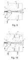
- FIG. 8 an illustration of an exemplary beam obtained by means of the focussing device of the atom probe according to the invention.
- FIG. 9 an illustration of another exemplary focussed beam obtained by means of the focussing device of the atom probe according to the invention.
- FIGS. 10 , 11 and 12 illustrations of a variant embodiment of the atom probe according to the invention.
- FIG. 13 the illustration of another variant embodiment of the atom probe according to the invention.
- FIGS. 1 to 3 diagrammatically show the basic structure of a tomographic atom probe, notably of an atom probe known as a “3D” probe. This type of probe is well known to those skilled in the art, so this document does not describe such a device in detail.
- FIGS. 1 to 3 however provide a review of the following points.
- a 3D tomographic atom probe is for analysing a sample of material 11 , atom layer after atom layer.
- it basically comprises a sample-holding device on which the sample 11 of material to be analysed is mounted, and a detector 12 situated at a predetermined distance L from the sample. It also comprises means (not shown in FIG. 1 ) for evaporating (separating), in ion form, the atoms forming the sample of material being analysed and accelerating them so that the duly released ions follow a trajectory that causes each evaporated ion 13 to strike the surface of the detector 12 at a given point 14 determined by the position of that ion on the surface of the sample before its separation.
- atom-by-atom erosion for reconstructing the composition of the sample, atom layer by atom layer, makes it possible to determine the composition in three dimensions of the sample concerned.
- the probe also comprises a vacuum chamber (not shown in FIG. 1 ), the potential of which is, for example, that of the ground of the system in which the probe is included.
- a device comprising a source of ions consisting of the sample 11 , an analysis chamber, or flight chamber, of length L (analysis length) and a planar detector 12 , the dimensions of which cover a circular surface of diameter D.
- the electrical field prevailing in the flight chamber varies in value and can, for example, be nil. In the latter case, the ions are propagated at constant speed inside the flight chamber.
- said detector When an ion arrives on the detector, said detector measures the position (x, y) on its surface of the point of incidence of the received ion.
- the detector also measures the “flight time”, a duration counted from the moment corresponding to the separation of the ion concerned.
- a geometrical correction is also applied so that the position of the point of impact can be taken into account in calculating the distance travelled between the point and the detector. Then, the position on the surface of the sample, occupied by the ion concerned before its separation, is deduced in a known manner from the position of its point of impact on the surface of the detector, by the application of a simple projection rule.
- the detector 12 determines the moment of arrival of the ion concerned, relative to a known time reference, usually corresponding to the moment at which the analysis of the sample 11 began. Measuring this moment advantageously gives the depth at which the ion concerned was situated relative to the initial surface of the sample and thus produces a true position in three dimensions of the atom from which the ion concerned in the sample 11 of material being analysed originates.
- the sample 11 is a piece of material in the shape of a substantially tapered point with an end forming a spherical cap of radius R which can vary during the analysis time.
- R radius of this spherical cap 21 , initially of a given value R 1 , has a value R 2 corresponding to the spherical cap 22 that exists at the end of the analysis; the erosion of the point at the same time causes an equivalent variation in the distance between the sample 11 and the detector 12 .
- a tomographic atom probe can also be characterized, in a known manner, by different parameters that are, notably, its magnification G, and by the potential difference V that should exist between the point 11 forming the sample and the inlet of the analysis chamber itself, the potential difference being responsible for the acceleration imparted on the evaporated ions to pass the electrical field to be applied through the analysis chamber of length L.
- the coefficient b which depends on the geometry of the instrumentation, point, detector and vacuum chamber is typically between 1 and 2.
- v the speed of displacement of the ions
- the mass resolution ⁇ M/M is proportional to the precision on the flight time ⁇ T/T, it is advantageous to have the greatest possible flight time T, and consequently the greatest possible distance L.
- the measurement of the flight time is essential in the instrument to identifying the ratio m/q of a detected ion, m being the mass of the ion and q its electrical charge, it is advantageous to increase the distance L between the sample and the detector in order to also increase the flight time.
- a device for focussing the beam of ions emitted by the sample 11 on the constructed detector 12 can, for example, be constructed as illustrated in FIG. 4 , using an electrostatic lens 41 , such as an “Einzel” lens, a device well known in charged particle optics, placed between the sample 11 and the detector 12 .
- an electrostatic lens 41 such as an “Einzel” lens, a device well known in charged particle optics, placed between the sample 11 and the detector 12 .
- the “Einzel” lens consisting of three electrodes 42 , 43 and 44 , placed on the path of the ions and configured to have a portion of the trajectory of these ions governed by an electrical field that acts directly on this trajectory.
- the initially divergent beam 45 is modified to a convergent beam 46 , the convergence obtained being a function of the intensity of the electrical field produced.
- the electrodes forming the lens are brought to appropriate potentials.
- the “Einzel” lens may comprise a first electrode 42 , placed in the vicinity of the sample 11 , itself grounded, then a second electrode 43 brought to a positive potential, then finally a third electrode 44 also brought to ground, so that, at the output of the lens, the ions pursue their trajectories in a space with no electrical field.
- the first electrode 42 also serves as the extracting electrode, or counter-electrode, or even local electrode, which is usually placed in the tomographic atom probes to locate the electrical field that produces the initial acceleration of the ions evaporated from the sample.
- Such a focussing device can advantageously be used to limit the percentage of ions whose trajectories do not encounter the detector.
- its efficiency remains generally limited by the fact that any electrostatic lens exhibits what is called a spherical aberration which is reflected in an overconvergence of the outer region of the lens and an overfocussing for the most off-centre trajectories because, as illustrated in FIGS. 5 and 6 (cross-sectional diagrammatic views) on two exemplary lens configurations, one and the same point 51 , 61 of the detector can intercept several distinct trajectories at a time, resulting in an indeterminacy concerning the origin position of an ion that has struck the detector at that point.
- this corresponds, for example, to an atom probe in which the sample 11 has its point brought to a voltage of 15 kV, whereas the first electrode 42 of the “Einzel” lens (closest to the sample), which is used as extracting electrode, is grounded, the second electrode 43 is brought to a voltage of 14 kV and the third electrode 44 (closest to the detector) is also grounded, just like the detector 12 .
- the relative dimensions of the second and third electrodes are such that, during most of their path, the ions remain subject to a focussing electrical field.
- the configuration of FIG. 6 corresponds, for example, to an atom probe in which the sample 11 has its point brought to a voltage of 15 kV, whereas the first electrode 42 of the “Einzel” lens (closest to the sample), which is used as extracting electrode, is grounded, the second electrode 43 is brought to a voltage of 12.5 kV and the third electrode 44 (closest to the detector) is also grounded, just like the detector 12 .
- the relative dimensions of the second and third electrodes are such that, during most of their path, the ions pass through a fieldless space, in which there is no focussing effect.
- FIGS. 7 and 8 present the structure of the atom probe according to the invention.
- Said atom probe has a general structure that is perfectly well known, with a sample holder for receiving the sample 11 of material to be analysed, and a detector 12 sensitive to the impacts of the ions evaporated from the sample and propelled against its sensitive surface.
- the probe according to the invention also comprises an accelerating electrode, or extractor, positioned close to the sample, and an electrostatic lens of “Einzel” type to focus the electron beam that is produced, consisting of three adjacent electrodes 71 , 72 and 73 , the first electrode of the “Einzel” lens consisting of the accelerating electrode.
- the electrodes of the electrostatic lens are polarized so that, given the respective biases of the sample and of the detector, the evaporated ions are initially accelerated towards the detector, and are then subject, during a part of their path, corresponding to the passage through the lens, to a focussing electrical field.
- the three electrodes are, moreover, preferentially configured and arranged in such a way as to provide in the flight chamber a free space that is sufficient to house a removable probe adjusting device.
- the adjusting device can, for example, be a field ion microscope.
- the area of the detector can, moreover, according to the embodiment concerned, be brought to an intermediate potential between that of the sample and that of the extracting electrode 71 .
- the potential concerned is set directly or via a grating arranged in proximity to the detector. According to a variant embodiment, this potential is that to which the extractor is brought.
- the electrodes of the electrostatic lens are formed by mechanical parts that have a central aperture and a symmetry of revolution about a central axis, combined with the axis 74 joining the tip of the point forming the sample 11 of material to the detector 12 and perpendicular to the plane of the detector.
- the first electrode 71 or extractor, situated in proximity to the sample 11 and serving as extracting electrode is preferentially a piece of small thickness having a hole 78 for the passage of the ions, a circular hole for example.
- the third electrode 73 of the electrostatic lens is any electrode, preferentially of relatively small thickness and having a central aperture 79 with a diameter greater than or at least roughly equal to the diameter D of the detector 12 , so as to allow for the propagation of the evaporated ions to the detector, and to do so regardless of the trajectory followed by these ions in the lens.
- the second electrode 72 central electrode of the lens, the latter has a shape defining an internal space whose dimensions advantageously vary over the length of the electrode.
- the second electrode 72 comprises a first segment 711 adjacent to the first electrode 71 and having a cylindrical aperture centred on the axis 74 , of a radius r 1 suitable for the passage of the beam of evaporated ions. It also comprises a second segment 712 , having a cylindrical aperture centred on the axis 74 and of radius r 2 , the radius r 2 adapted to the width of the beam being greater than the radius r 1 . It also comprises a third segment 713 , having a tapered aperture linking the aperture of the first segment to that of the second segment.
- the profile 75 of the inner surface of the second electrode describes a broken line passing through the three points M 1 (z 1 , M 2 (z 2 , r 2 ), M 3 (z 3 , r 3 ).
- z 1 , z 2 and z 3 represent the abscissae on the axis 74 of the points M 1 , M 2 and M 3 relative to an origin O of abscissa z 0 situated at the point of the sample of material 11 and represented in the figure by the intersection of the axes 74 and 714 .
- condition g) amounts to stating that all the points of the cross-sectional profile 75 of the electrode situated between M 1 and M 3 should be situated outside the area of the cross-sectional plane delimited by the profile of a cone limited by the points M 2 and M 3 .
- the probe according to the invention makes it possible to very significantly increase the analysis length that can be used.
- the intensity of the focussing is still defined by the value of the bias voltages applied to the different electrodes of the focussing lens produced.
- the ion beam will be more or less focussed, the objective being, however, for the focussed beam to cover the greatest possible surface area on the detector.
- the focussed ion beam can then, for example, depending on the case, take the form of the beam 81 illustrated in FIG. 8 , or even that of the beam 91 illustrated in FIG. 9 . In the case of FIG.
- the beam 81 is obtained by applying, for example, a voltage of 13.7 kV to the second electrode 72 and grounding the first and third electrodes, the detector also being grounded and the sample being brought to a voltage of 15 kV.
- the beam 91 is obtained by applying, for example, a voltage of 15.1 kV to the second electrode 72 and by grounding the first and third electrodes, the detector and the sample, as in the preceding case, also being respectively grounded and brought to a voltage of 15 kV.
- the architecture of the atom probe according to the invention corresponds to a basic common architecture, the probe according to the invention being able, in practice, to comprise certain variant embodiments corresponding to specific applications such as those presented in a nonlimiting manner hereinafter in the description.
- the first electrode 71 forming the focussing lens, the extracting electrode comprises a central aperture 78 equipped with a device with multiple apertures.
- This device consists, as illustrated in FIG. 12 , of a strip of diaphragms 112 arranged in such a way as to slide in front of the central aperture 78 of the electrode 71 .
- the diameters of the different diaphragms 111 of the strip 112 are defined in such a way as to reduce to a greater or lesser degree the diameter of the orifice for the passage of the ions emitted by the sample 11 .
- the diameter d of the aperture of the extractor is thus adapted to intercept the peripheral part of the beam of emitted ions so as to block the ions that have the most peripheral trajectories.
- the various diaphragms are arranged on the strip so that the distance between two contiguous diaphragms is sufficient for all except the diaphragm being used to be perfectly masked by the electrode.
- the positioning in the two dimensions perpendicular to the axis of the beam can, moreover, be obtained by an appropriate mechanism, possibly controlled by a computer and arranged outside the chamber of the probe.
- the atom probe according to the invention comprises a second focussing lens, of the “Einzel” lens type for example, placed between the first lens and the detector.
- This particular configuration makes it possible to apply a compensation for the residual spherical aberration presented by the first focussing lens, despite its particular configuration, this spherical aberration of the first lens not always being able to be avoided.
- the atom probe according to the invention comprises, in addition to the three electrodes 71 , 72 and 73 forming the first lens, two complementary electrodes 132 and 133 , the electrode 132 being placed adjacent to the electrode 73 and the electrode 133 being placed adjacent to the electrode 132 , between that electrode and the detector 12 .
- the electrode 133 is brought to a potential roughly equal to that of the electrode 73 , whereas the electrode 132 is brought to a potential enabling all three electrodes 73 , 132 and 133 to thus form a second electrostatic lens containing an electrical field.
- the second electrode 72 of the first lens and the second electrode 131 of the second lens are brought to potentials defined to:
- the electrical field applied to the ion beam inside the second electrostatic lens can, depending on the scenario envisaged, be an accelerating or delaying field.
- Such a device can, for example, be obtained from a structure such as that illustrated by FIG. 13 .
- the extracting electrode 71 is then grounded, as are the electrodes 73 and 133 , whereas the central electrode 72 of the first lens is brought to a voltage of 15.3 kV and the central electrode 132 of the second lens is brought to a voltage of 14.5 kV.
Landscapes
- Chemical & Material Sciences (AREA)
- Analytical Chemistry (AREA)
- Physics & Mathematics (AREA)
- Spectroscopy & Molecular Physics (AREA)
- Other Investigation Or Analysis Of Materials By Electrical Means (AREA)
Abstract
Description
-
- a sample-holding device for receiving a sample of material to be analysed having an extraction area of substantially pointed shape,
- a position- and time-sensitive detector, of useful diameter D, and spaced apart from the sample by a distance L;
- an electrostatic lens consisting of three electrodes, a first electrode or extractor, arranged in proximity to the sample, an intermediate second electrode, and a third electrode arranged between the intermediate electrode and the detector, the three electrodes having a symmetry of revolution about the axis Oz passing through the point of the sample and perpendicular to the plane P of the detector;
and characterized in that, since the distance L is greater than 2.75 D, the respective potentials of the sample, of the first electrode of the lens and of the detector are such that the ions deriving from the sample mounted on the sample-holder are attracted towards the first electrode and towards the detector; the cross-sectional profile of the intermediate electrode, in a cross-sectional plane rOz defining three points M1, M2 and M3 of respective coordinates (r1, (r2, z2) and (r3, z3) relative to an origin z0 on the point of the sample, which satisfy the following conditions, it being understood that the positive direction along the axis Oz goes from the sample to the detector:
z1<z2<z3,
|z 1 −z 0 |<D/3,
|z 2 −z 1<0.65·D,
z 3 −z 1>1.4·D,
r2=r1,
0.1·D<r 1<0.65·D,
D<r 3<1.6·D;
all the points of the cross-sectional profile of the electrode being situated outside the area of the cross-sectional plane delimited by the profile of a cone with cylindrical tip limited by the points M1, M2 and M3.
in which M represents the mass of the ion, v its speed, n the number of individual charges borne by the ion; e the elementary charge, that is to say the charge of the electron, and V the acceleration voltage applied. Therefore, the flight time of an ion being given by the relation:
the mass of the ion will be determined according to the flight time, according to the relation:
0;1·D<r 1<0.65·D a)
r2=r1 b)
D<r 2<1.6·D c)
|z 1 −z 0 |<D/3 d)
|z 2 −z 1<0;65·D e)
|z 3 −z 1|<1.4·D f)
g) at any point Mi(ri, zi) of the area M2M3 of the
-
- produce, with the help of the first lens, the focussing of the trajectories of small aperture on the median plane of the second lens, represented by the dotted line 134 in
FIG. 13 . In this way, the second lens, consisting of theelectrodes 73, 132 and 133, has no effect on the trajectories of small aperture. - apply, with the help of the first lens, an overfocussing of the trajectories of greater apertures. The aberrations that then appear are corrected by applying the appropriate potential to the central electrode 132 of the second lens.
- produce, with the help of the first lens, the focussing of the trajectories of small aperture on the median plane of the second lens, represented by the dotted line 134 in
Claims (14)
z1<z2<z3,
|z 1 −z 0 |<D/3,
|z 2 −z 1|<0.65·D,
|z 3 −z 1>1.4·D,
r2=r1,
0.1·D<r 1<0.65·D,
D<r 3<1.6·D;
Applications Claiming Priority (3)
| Application Number | Priority Date | Filing Date | Title |
|---|---|---|---|
| FR0707178A FR2922350B1 (en) | 2007-10-12 | 2007-10-12 | HIGH ANGLE TOMOGRAPHIC PROBE WITH HIGH RESOLUTION. |
| FR0707178 | 2007-10-12 | ||
| PCT/EP2008/063462 WO2009047265A1 (en) | 2007-10-12 | 2008-10-08 | Wide angle high resolution tomographic probe |
Publications (2)
| Publication Number | Publication Date |
|---|---|
| US20100223698A1 US20100223698A1 (en) | 2010-09-02 |
| US8074292B2 true US8074292B2 (en) | 2011-12-06 |
Family
ID=39167016
Family Applications (1)
| Application Number | Title | Priority Date | Filing Date |
|---|---|---|---|
| US12/682,700 Active 2028-12-11 US8074292B2 (en) | 2007-10-12 | 2008-10-08 | High resolution wide angle tomographic probe |
Country Status (4)
| Country | Link |
|---|---|
| US (1) | US8074292B2 (en) |
| EP (1) | EP2198449B1 (en) |
| FR (1) | FR2922350B1 (en) |
| WO (1) | WO2009047265A1 (en) |
Cited By (5)
| Publication number | Priority date | Publication date | Assignee | Title |
|---|---|---|---|---|
| US20110260046A1 (en) * | 2008-11-21 | 2011-10-27 | Cnrs | Tomographic Atom Probe Comprising an Electro-Optical Generator of High-Voltage Electrical Pulses |
| DE112018000062T5 (en) | 2018-01-31 | 2019-09-19 | Cameca Instruments, Inc. | ENERGY RADIATION INPUT TO ATOMIC SAMPLE SAMPLES FROM DIFFERENT ANGLES |
| US10614995B2 (en) | 2016-06-27 | 2020-04-07 | Cameca Instruments, Inc. | Atom probe with vacuum differential |
| US10615001B2 (en) | 2015-04-21 | 2020-04-07 | Cameca Instruments, Inc. | Wide field-of-view atom probe |
| US11087956B2 (en) * | 2018-06-29 | 2021-08-10 | Taiwan Semiconductor Manufacturing Co., Ltd. | Detection systems in semiconductor metrology tools |
Families Citing this family (1)
| Publication number | Priority date | Publication date | Assignee | Title |
|---|---|---|---|---|
| JP6204367B2 (en) * | 2011-10-28 | 2017-09-27 | レコ コーポレイションLeco Corporation | Electrostatic ion mirror |
Citations (3)
| Publication number | Priority date | Publication date | Assignee | Title |
|---|---|---|---|---|
| US20060113470A1 (en) * | 2003-06-06 | 2006-06-01 | Gribb Tye T | High resolution atom probe |
| JP2007040966A (en) | 2005-06-28 | 2007-02-15 | Fujitsu Ltd | Three-dimensional atom level structure observation device |
| US20070073364A1 (en) * | 2005-09-29 | 2007-03-29 | Siemens Aktiengesellschaft | Combined OCT catheter device and method for combined optical coherence tomography (OCT) diagnosis and photodynamic therapy (PDT) |
-
2007
- 2007-10-12 FR FR0707178A patent/FR2922350B1/en not_active Expired - Fee Related
-
2008
- 2008-10-08 EP EP08838185.0A patent/EP2198449B1/en active Active
- 2008-10-08 WO PCT/EP2008/063462 patent/WO2009047265A1/en active Application Filing
- 2008-10-08 US US12/682,700 patent/US8074292B2/en active Active
Patent Citations (3)
| Publication number | Priority date | Publication date | Assignee | Title |
|---|---|---|---|---|
| US20060113470A1 (en) * | 2003-06-06 | 2006-06-01 | Gribb Tye T | High resolution atom probe |
| JP2007040966A (en) | 2005-06-28 | 2007-02-15 | Fujitsu Ltd | Three-dimensional atom level structure observation device |
| US20070073364A1 (en) * | 2005-09-29 | 2007-03-29 | Siemens Aktiengesellschaft | Combined OCT catheter device and method for combined optical coherence tomography (OCT) diagnosis and photodynamic therapy (PDT) |
Non-Patent Citations (2)
| Title |
|---|
| A. Cerezo, et al., "Design of a Scanning Atom Probe with Improved Mass Resolution", Review of Scientific Instruments, Aug. 1, 2000, pp. 3016-3023, vol. 71,No. 8, American Institute of Physics, Melville, NY, USA. XP012038436. |
| A. Cerezo, et al., "Einzel Lenses in Atom Probe Designs", Surface Science Netherlands, Apr. 1991, pp. 460-466, vol. 246, No. 1-3. XP007904810. |
Cited By (6)
| Publication number | Priority date | Publication date | Assignee | Title |
|---|---|---|---|---|
| US20110260046A1 (en) * | 2008-11-21 | 2011-10-27 | Cnrs | Tomographic Atom Probe Comprising an Electro-Optical Generator of High-Voltage Electrical Pulses |
| US8276210B2 (en) * | 2008-11-21 | 2012-09-25 | Cameca | Tomographic atom probe comprising an electro-optical generator of high-voltage electrical pulses |
| US10615001B2 (en) | 2015-04-21 | 2020-04-07 | Cameca Instruments, Inc. | Wide field-of-view atom probe |
| US10614995B2 (en) | 2016-06-27 | 2020-04-07 | Cameca Instruments, Inc. | Atom probe with vacuum differential |
| DE112018000062T5 (en) | 2018-01-31 | 2019-09-19 | Cameca Instruments, Inc. | ENERGY RADIATION INPUT TO ATOMIC SAMPLE SAMPLES FROM DIFFERENT ANGLES |
| US11087956B2 (en) * | 2018-06-29 | 2021-08-10 | Taiwan Semiconductor Manufacturing Co., Ltd. | Detection systems in semiconductor metrology tools |
Also Published As
| Publication number | Publication date |
|---|---|
| EP2198449A1 (en) | 2010-06-23 |
| FR2922350A1 (en) | 2009-04-17 |
| EP2198449B1 (en) | 2018-01-24 |
| US20100223698A1 (en) | 2010-09-02 |
| FR2922350B1 (en) | 2009-12-04 |
| WO2009047265A1 (en) | 2009-04-16 |
Similar Documents
| Publication | Publication Date | Title |
|---|---|---|
| US8074292B2 (en) | High resolution wide angle tomographic probe | |
| US5128543A (en) | Particle analyzer apparatus and method | |
| US8134119B2 (en) | Reflectron | |
| US8513597B2 (en) | Atom probe | |
| US7227142B2 (en) | Dual detector optics for simultaneous collection of secondary and backscattered electrons | |
| US20110278454A1 (en) | Scanning electron microscope | |
| US10614992B2 (en) | Electrostatic lens, and parallel beam generation device and parallel beam convergence device which use electrostatic lens and collimator | |
| JP2005534041A (en) | A method for local high-resolution surface mass spectroscopic characterization using scanning probe technology | |
| JPH0441462B2 (en) | ||
| EP2355125B1 (en) | Particle beam device and method for operation of a particle beam device | |
| US5220167A (en) | Multiple ion multiplier detector for use in a mass spectrometer | |
| US8502139B2 (en) | Mass analysis device with wide angular acceptance including a reflectron | |
| US10615001B2 (en) | Wide field-of-view atom probe | |
| GB2426120A (en) | A reflectron for use in a three-dimensional atom probe | |
| US9679756B2 (en) | Projection-type charged particle optical system and imaging mass spectrometry apparatus | |
| US8803087B2 (en) | Spectrum analyzer and method of spectrum analysis | |
| JPS63276860A (en) | Surface analyzing device | |
| CN109632939A (en) | A kind of method and its system using ion probe measurement inert gas | |
| Heller et al. | Backscattering spectrometry in the helium ion microscope: Imaging elemental compositions on the nm scale | |
| JPH06325719A (en) | Charged particle beam device | |
| TW201941247A (en) | Apparatus and method for measuring energy spectrum of reflected electrons | |
| KR100687074B1 (en) | System for analysis of thin film using the scattering of focused ion beam | |
| US11898975B2 (en) | Electron spectrometer | |
| JPS60240043A (en) | Energy analyzer | |
| JPH11111209A (en) | Polarization analyzer and analyzing device |
Legal Events
| Date | Code | Title | Description |
|---|---|---|---|
| AS | Assignment |
Owner name: CAMECA, FRANCE Free format text: ASSIGNMENT OF ASSIGNORS INTEREST;ASSIGNORS:BOSTEL, ALAIN;YAVOR, MIKHAIL;RENAUD, LUDOVIC;AND OTHERS;SIGNING DATES FROM 20100413 TO 20100414;REEL/FRAME:024250/0177 Owner name: CENTRE NATIONAL DE LA RECHERCHE SCIENTIFIQUE, FRAN Free format text: ASSIGNMENT OF ASSIGNORS INTEREST;ASSIGNORS:BOSTEL, ALAIN;YAVOR, MIKHAIL;RENAUD, LUDOVIC;AND OTHERS;SIGNING DATES FROM 20100413 TO 20100414;REEL/FRAME:024250/0177 |
|
| STCF | Information on status: patent grant |
Free format text: PATENTED CASE |
|
| FPAY | Fee payment |
Year of fee payment: 4 |
|
| MAFP | Maintenance fee payment |
Free format text: PAYMENT OF MAINTENANCE FEE, 8TH YEAR, LARGE ENTITY (ORIGINAL EVENT CODE: M1552); ENTITY STATUS OF PATENT OWNER: LARGE ENTITY Year of fee payment: 8 |
|
| MAFP | Maintenance fee payment |
Free format text: PAYMENT OF MAINTENANCE FEE, 12TH YEAR, LARGE ENTITY (ORIGINAL EVENT CODE: M1553); ENTITY STATUS OF PATENT OWNER: LARGE ENTITY Year of fee payment: 12 |