US8072787B2 - Synchronous rectifying for soft switching power converters - Google Patents
Synchronous rectifying for soft switching power converters Download PDFInfo
- Publication number
- US8072787B2 US8072787B2 US11/924,761 US92476107A US8072787B2 US 8072787 B2 US8072787 B2 US 8072787B2 US 92476107 A US92476107 A US 92476107A US 8072787 B2 US8072787 B2 US 8072787B2
- Authority
- US
- United States
- Prior art keywords
- signal
- power transistor
- power
- switching
- threshold
- Prior art date
- Legal status (The legal status is an assumption and is not a legal conclusion. Google has not performed a legal analysis and makes no representation as to the accuracy of the status listed.)
- Active, expires
Links
- 230000001360 synchronised effect Effects 0.000 title claims abstract description 55
- 238000004804 winding Methods 0.000 claims abstract description 26
- 230000003071 parasitic effect Effects 0.000 claims description 2
- 238000000034 method Methods 0.000 claims 1
- 239000003990 capacitor Substances 0.000 description 19
- 238000010586 diagram Methods 0.000 description 3
- 230000001276 controlling effect Effects 0.000 description 2
- 230000002596 correlated effect Effects 0.000 description 2
- 238000001514 detection method Methods 0.000 description 2
- 238000012986 modification Methods 0.000 description 2
- 230000004048 modification Effects 0.000 description 2
- 238000002955 isolation Methods 0.000 description 1
Images


Classifications
-
- H—ELECTRICITY
- H02—GENERATION; CONVERSION OR DISTRIBUTION OF ELECTRIC POWER
- H02M—APPARATUS FOR CONVERSION BETWEEN AC AND AC, BETWEEN AC AND DC, OR BETWEEN DC AND DC, AND FOR USE WITH MAINS OR SIMILAR POWER SUPPLY SYSTEMS; CONVERSION OF DC OR AC INPUT POWER INTO SURGE OUTPUT POWER; CONTROL OR REGULATION THEREOF
- H02M3/00—Conversion of DC power input into DC power output
- H02M3/22—Conversion of DC power input into DC power output with intermediate conversion into AC
- H02M3/24—Conversion of DC power input into DC power output with intermediate conversion into AC by static converters
- H02M3/28—Conversion of DC power input into DC power output with intermediate conversion into AC by static converters using discharge tubes with control electrode or semiconductor devices with control electrode to produce the intermediate AC
- H02M3/325—Conversion of DC power input into DC power output with intermediate conversion into AC by static converters using discharge tubes with control electrode or semiconductor devices with control electrode to produce the intermediate AC using devices of a triode or a transistor type requiring continuous application of a control signal
- H02M3/335—Conversion of DC power input into DC power output with intermediate conversion into AC by static converters using discharge tubes with control electrode or semiconductor devices with control electrode to produce the intermediate AC using devices of a triode or a transistor type requiring continuous application of a control signal using semiconductor devices only
- H02M3/33569—Conversion of DC power input into DC power output with intermediate conversion into AC by static converters using discharge tubes with control electrode or semiconductor devices with control electrode to produce the intermediate AC using devices of a triode or a transistor type requiring continuous application of a control signal using semiconductor devices only having several active switching elements
- H02M3/33576—Conversion of DC power input into DC power output with intermediate conversion into AC by static converters using discharge tubes with control electrode or semiconductor devices with control electrode to produce the intermediate AC using devices of a triode or a transistor type requiring continuous application of a control signal using semiconductor devices only having several active switching elements having at least one active switching element at the secondary side of an isolation transformer
- H02M3/33592—Conversion of DC power input into DC power output with intermediate conversion into AC by static converters using discharge tubes with control electrode or semiconductor devices with control electrode to produce the intermediate AC using devices of a triode or a transistor type requiring continuous application of a control signal using semiconductor devices only having several active switching elements having at least one active switching element at the secondary side of an isolation transformer having a synchronous rectifier circuit or a synchronous freewheeling circuit at the secondary side of an isolation transformer
-
- Y—GENERAL TAGGING OF NEW TECHNOLOGICAL DEVELOPMENTS; GENERAL TAGGING OF CROSS-SECTIONAL TECHNOLOGIES SPANNING OVER SEVERAL SECTIONS OF THE IPC; TECHNICAL SUBJECTS COVERED BY FORMER USPC CROSS-REFERENCE ART COLLECTIONS [XRACs] AND DIGESTS
- Y02—TECHNOLOGIES OR APPLICATIONS FOR MITIGATION OR ADAPTATION AGAINST CLIMATE CHANGE
- Y02B—CLIMATE CHANGE MITIGATION TECHNOLOGIES RELATED TO BUILDINGS, e.g. HOUSING, HOUSE APPLIANCES OR RELATED END-USER APPLICATIONS
- Y02B70/00—Technologies for an efficient end-user side electric power management and consumption
- Y02B70/10—Technologies improving the efficiency by using switched-mode power supplies [SMPS], i.e. efficient power electronics conversion e.g. power factor correction or reduction of losses in power supplies or efficient standby modes
Definitions
- the present invention relates to power converters, and more particularly, relates to synchronous rectifying for soft switching power converters.
- FIG. 1 shows a circuit schematic of a conventional soft switching power converter 1 . It includes a transformer 10 to provide isolation from line input V IN to the output V O of the power converter 1 for safety. Switches 20 and 30 develop a half bridge circuit to switch a resonant tank and the transformer 10 . An inductor 5 and a capacitor 40 form the resonant tank.
- the inductor 5 can be an inductance device or the leakage inductance of a primary winding N P of the transformer 10 .
- the inductance L of the inductor 5 and the capacitance C of the capacitor 40 determine the resonance frequency f 0 of the resonant tank.
- the transformer 10 transfers the energy from the primary winding N P to the secondary windings N S1 , N S2 of the transformer 10 .
- Rectifiers 61 , 62 and a capacitor 65 rectify and filter voltages at the secondary windings N S1 , N S2 to generate a DC voltage V O at the output of the power converter 1 .
- the detail operation and description of the soft switching power converter 1 can be found in text book “Resonant Power Converters” by Marian K. Kazimierczuk and Dariusz Czarkowski, 1995 by John Wiley & Sons, Inc.
- the soft switching of the power converter can achieve high efficiency and low EMI (electric-magnetic interference) performance
- the forward voltage of rectifiers 61 and 62 still causes significant power losses.
- Using transistors as the synchronous rectifiers is a higher efficiency approach, such as “Control circuit associated with saturable inductor operated as synchronous rectifier forward power converter” disclosed by Yang, in U.S. Pat. No. 7,173,835.
- the disadvantage of this prior art is an additional power consumptions caused by saturable inductors, etc. Besides, it is not optimized for soft-switching topologies.
- the object of present invention is to provide the synchronous rectifying for soft switching power converter to achieve higher efficiency.
- a synchronous rectifying apparatus or circuit for a soft switching power converter includes: a power transistor and a diode connected from a transformer to the output of the power converter for the rectifying; a controller, having a latch circuit, for generating a drive signal to control the power transistor in response to a switching signal which is generated by a winding of the transformer and responsive to the switching of the transformer.
- the switching signal is correlated to the zero-crossings of the switching current of the transformer.
- the controller is developed to turn off the power transistor when the switching signal is lower than a low-threshold or the diode is reversely biased.
- the power transistor is turned on when the switching signal is higher than a high-threshold and the diode is forward biased.
- the level of the high-threshold is higher than the level of the low-threshold.
- a maximum-on-time circuit of the controller is utilized to limit the maximum on time of the power transistor.
- FIG. 1 shows a circuit schematic of a conventional soft switching power converter.
- FIG. 2 shows a preferred embodiment of integrated synchronous rectifiers for a soft switching power converter according to the present invention.
- FIG. 3 is a schematic diagram of an integrated synchronous rectifier according to an embodiment of the present invention.
- FIG. 4 is an embodiment of a controller of the integrated synchronous rectifier according to the present invention.
- FIG. 5 is a maximum-on-time (MOT) circuit according to an embodiment of the present invention.
- FIG. 6 shows key waveforms of the synchronous rectifying according to the present invention.
- FIG. 7 is a preferred embodiment of a monitor circuit according to the present invention.
- FIG. 8 shows another preferred embodiment of integrated synchronous rectifiers for soft switching power converter according to the present invention.
- FIG. 2 shows a soft switching power converter 2 with integrated synchronous rectifier (synchronous rectifying circuit) according to an embodiment of the invention.
- the power converter 2 includes a transformer 15 having a primary winding N P , secondary windings N S1 , N S2 and an auxiliary winding N S3 .
- the primary winding N P of the transformer 15 is coupled to two switches 20 and 30 which switch the primary winding N P of the transformer 15 .
- the transformer 15 operates in a switching mode.
- Switches 20 and 30 develop a half bridge circuit to switch a resonant tank and the transformer 15 .
- An inductor 5 and a capacitor 40 form the resonant tank.
- the transformer 15 transfers the energy from the primary winding N P to the secondary windings N S1 , N S2 of the transformer 15 .
- Integrated synchronous Rectifiers 51 , 52 and a capacitor 65 rectify and filter voltages at the secondary windings N S1 , N S2 to generate a DC voltage V O at the output of the power converter 2 .
- the integrated synchronous rectifier 51 has a cathode terminal K connected to the secondary winding N S1 .
- An anode terminal A of the integrated synchronous rectifier 51 is connected to the output ground of the power converter 2 .
- An integrated synchronous rectifier 52 having the cathode terminal K and the anode terminal A is also connected from the secondary winding N S2 to the output ground of the power converter 2 .
- An input-signal terminal X, an input-signal terminal Y of the integrated synchronous rectifier 51 and the integrated synchronous rectifier 52 are connected to the auxiliary winding N S3 to receive a switching signal V S .
- the switching signal V S is used for controlling the integrated synchronous rectifiers 51 and 52 .
- the switching signal V S is generated in response to the switching of the transformer 15 .
- the switching signal V S is correlated to switching currents I S1 and I S2 of the transformer 15 .
- the auxiliary winding N S3 thus generates the switching signal V S in response to the zero-crossings of the switching current I S1 or I S2 .
- the switching signal V S is a differential signal.
- the polarity of the switching signal V S determines turning on or turning off of the integrated synchronous rectifiers 51 and 52 .
- a power-good signal P G is generated by the integrated synchronous rectifiers 51 and 52 .
- the power-good signal P G is disabled when the amplitude of the switching signal V S is lower than a threshold voltage or a supply voltage VCC at terminal VCC of the integrated synchronous rectifier 51 or 52 is lower than a VCC threshold.
- FIG. 3 is the schematic diagram of an integrated synchronous rectifier 50 showing an exemplary implementation of the integrated synchronous rectifier 51 or 52 .
- the integrated synchronous rectifier 50 includes a power transistor 200 , a diode 250 and a controller 100 .
- the diode 250 is connected to the power transistor 200 in parallel, which is a Schottky diode or a parasitic device of the power transistor 200 for example.
- the power transistor 200 is connected between the cathode terminal K and the anode terminal A of the integrated synchronous rectifier 50 .
- the cathode terminal K is coupled to the secondary winding (N S1 or N S2 ) of the transformer 15 .
- the anode terminal A is coupled to the output (V O ) of the power converter 2 .
- the controller 100 receives the switching signal V S via input-signal terminals X and Y for turning on or turning off the power transistor 200 .
- a VCC terminal is utilized to supply the power source to the controller 200 .
- a power-good terminal T PG outputs the power-good signal P G to show the operating status.
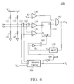
- FIG. 4 shows a schematic diagram of a preferred embodiment of the controller 100 .
- Resistors 111 and 121 provide a bias termination for the input-signal terminal X.
- Resistors 113 and 123 provide another bias termination for the input-signal terminal Y.
- the input-signal terminal X is coupled to the positive input of a comparator 110 through offset voltages 115 and 125 .
- the offset voltages 115 and 125 are coupled in serial.
- the input-signal terminal X is also coupled to the negative input of a comparator 120 via the offset voltage 115 .
- the input-signal terminal Y is connected to the positive input of the comparator 120 and the negative input of the comparator 110 .
- the offset voltages 115 and 125 produce hysteresis.
- a third comparator 130 having a threshold V TH connects to its positive input.
- the negative input of the comparator 130 is coupled to the cathode terminal K.
- the output of comparators 110 is coupled to the set-input terminal (“S”) of a SR flip-flop 150 .
- the reset-input terminal (“R”) of the SR flip-flop 150 is controlled by the output of the comparator 120 .
- the output of the SR flip-flop 150 and the output of the comparator 130 are connected to an AND gate 162 .
- a gate-drive signal V G is generated at the output of the AND gate 162 for controlling the power transistor 200 (shown in FIG. 3 ).
- the maximum on time of the gate-drive signal V G is limited by a maximum-on-time circuit (MOT) 170 .
- MOT maximum-on-time circuit
- the gate-drive signal V G is connected to the input of the maximum-on-time circuit 170 . After a blanking time, a maximum-on-time signal S M will be produced in response to the enabling of the gate-drive signal V G .
- the maximum-on-time signal S M is coupled to an AND gate 160 via an inverter 161 .
- Another input of the AND gate 160 is coupled to received a reset signal RST.
- the output of the AND gate 160 is coupled to the clear terminal (“CLR”) of the SR flip-flop 150 to clear the SR flip-flop 150 .
- the maximum on time of the gate-drive signal V G is thus limited by the blanking time of the maximum-on-time circuit 170 .
- the gate-drive signal V G will turn on the power transistor 200 when following equations (2) and (3) are met, V X ⁇ V Y >V 115 +V 125 (2) V K ⁇ V TH (3)
- the gate-drive signal V G will turn off the power transistor 200 when the switching signal V S is lower than the offset voltage 115 , i.e., when V X ⁇ V Y ⁇ V 115 .
- V X is the voltage of the input-signal terminal X
- V Y is the voltage of the input-signal terminal Y
- V K is the voltage of the cathode terminal K.
- V TH is the voltage of the threshold V TH
- V 115 is the value of the offset voltage 115
- V 125 is the value of the offset voltage 125 .
- the voltage of the cathode terminal K will be lower than the voltage of the threshold V TH when the diode 250 is forward biased and conducted. Therefore, the power transistor 200 can only be turned on after the diode 250 is turned on, which achieves the soft-switching of the power transistor 200 . Furthermore, the gate-drive signal V G will be disabled and the power transistor 200 will be turned off when the diode 250 is reversely biased (or when V K >V TH ).
- a monitor circuit 300 is coupled to the terminals X, Y and VCC, and detects the switching signal V S and the supply voltage VCC for generating the power-good signal P G .
- the reset signal RST is further produced by inverting the power-good signal P G via an inverter 180 .
- the reset signal RST is coupled to turn off the power transistor 200 , through the AND gate 160 , the SR flip-flop 150 and the AND gate 162 , when the monitor circuit 300 detects that the amplitude of the switching signal V S is lower than a predetermined threshold voltage or the supply voltage VCC is lower than a VCC threshold.
- FIG. 5 is the maximum-on-time circuit (MOT) 170 .
- a current source 173 is connected to charge a capacitor 175 .
- a transistor 172 is connected to discharge the capacitor 175 .
- the gate-drive signal V G is connected to control the transistor 172 through an inverter 171 .
- the gate-drive signal V G is further connected to an AND gate 179 .
- Another input of the AND gate 179 is coupled to the capacitor 175 .
- the output of the AND gate 179 will generate the maximum-on-time signal S M to disable the gate-drive signal V G after the blanking time.
- the blanking time is determined by the current of the current source 173 and the capacitance of the capacitor 175 .
- FIG. 6 shows key waveforms of the synchronous rectifying.
- the switching signal V S is generated in response to the zero-crossings of the switching current I S of the transformer 15 including I S1 and I S2
- the gate-drive signals V G1 and V G2 are the gate-drive signal V G of the integrated synchronous rectifier 51 and the integrated synchronous rectifier 52 respectively.
- FIG. 7 shows a preferred embodiment of the monitor circuit 300 .
- Current sources 320 , 325 and a capacitor 330 form a debounce circuit.
- the current source 320 is applied to charge the capacitor 330 .
- the current source 325 is coupled to discharge the capacitor 330 through a switch 315 .
- the turning on/off of the switch 315 is controlled by a comparator 310 .
- the positive input of the comparator 310 is coupled to the input-signal terminal X through the predetermined threshold voltage 305 .
- the negative input of the comparator 310 is connected to the input-signal terminal Y to receive the switching signal V S .
- the switch 315 is turned off and the capacitor 330 is charged when the switching signal V S is smaller than the threshold voltage 305 (i.e., when V X ⁇ V Y ⁇ V 305 ).
- the power-good signal P G will be disabled (logic “high”).
- An inverter 361 is connected to the capacitor 330 .
- the output of the inverter 361 is connected to an AND gate 365 .
- the output of the AND gate 365 generates the power-good signal P G via an inverter 370 .
- the VCC-detection circuit 390 is formed by transistors 351 , 353 , zener diodes 341 , 342 , resistors 352 , 345 , 346 and a capacitor 347 .
- VCC voltage is higher than the voltages of zener diodes 341 and 342 , a signal on resistor 345 will turn on the transistor 353 .
- the resistor 346 and the capacitor 347 are utilized to filter the noise of the signal on the resistor 345 .
- the output of the transistor 353 is connected to the input of the inverter 362 and the transistor 351 .
- the resistor 352 provides the bias for transistor 351 .
- the transistor 351 operates to short-circuit the zener diode 341 when the transistor 353 is turned on. After short-circuiting the zener diode 341 , the transistor 353 is subsequently turned off when the VCC voltage is lower than the voltage of zener diode 342 . Therefore, the power-good signal P G will be disabled (logic high) when the amplitude of the switching signal V S is lower than the threshold voltage 305 or the VCC supply voltage is lower than the voltage of zener diode 342 .
- FIG. 8 shows a soft switching power converter 8 with integrated synchronous rectifier (synchronous rectifying circuit) according to another embodiment of the invention. It is noted that similar or same components or devices in FIG. 8 and FIG. 2 are indicated by the same notations or numerals and may not be described in detail for brevity.
- the transformer 17 provides an auxiliary winding N A1 for generating a switching signal coupled to the integrated synchronous rectifier 51 through a resistor 75 .
- the auxiliary winding N A1 further generates a supply voltage (VCC) for the integrated synchronous rectifier 51 via a diode 71 and a capacitor 61 .
- An auxiliary winding N A2 of the transformer 17 generates another switching signal coupled to the integrated synchronous rectifier 52 through a resistor 76 .
- the auxiliary winding N A2 generates another supply voltage (VCC) for the integrated synchronous rectifier 52 via a diode 72 and a capacitor 62 .
Landscapes
- Engineering & Computer Science (AREA)
- Power Engineering (AREA)
- Dc-Dc Converters (AREA)
Abstract
Description
V X −V Y >V 115 +V 125 (2)
V K <V TH (3)
The gate-drive signal VG will turn off the
Claims (10)
Priority Applications (3)
| Application Number | Priority Date | Filing Date | Title |
|---|---|---|---|
| US11/924,761 US8072787B2 (en) | 2007-10-26 | 2007-10-26 | Synchronous rectifying for soft switching power converters |
| CN200810003318XA CN101232248B (en) | 2007-10-26 | 2008-01-16 | Synchronous rectification device, circuit and method for flexible switching power converter |
| TW097110047A TWI371907B (en) | 2007-10-26 | 2008-03-21 | Synchronous rectifying apparatus, circuit and method of soft switching power converter |
Applications Claiming Priority (1)
| Application Number | Priority Date | Filing Date | Title |
|---|---|---|---|
| US11/924,761 US8072787B2 (en) | 2007-10-26 | 2007-10-26 | Synchronous rectifying for soft switching power converters |
Publications (2)
| Publication Number | Publication Date |
|---|---|
| US20090109715A1 US20090109715A1 (en) | 2009-04-30 |
| US8072787B2 true US8072787B2 (en) | 2011-12-06 |
Family
ID=39898483
Family Applications (1)
| Application Number | Title | Priority Date | Filing Date |
|---|---|---|---|
| US11/924,761 Active 2029-01-17 US8072787B2 (en) | 2007-10-26 | 2007-10-26 | Synchronous rectifying for soft switching power converters |
Country Status (3)
| Country | Link |
|---|---|
| US (1) | US8072787B2 (en) |
| CN (1) | CN101232248B (en) |
| TW (1) | TWI371907B (en) |
Cited By (2)
| Publication number | Priority date | Publication date | Assignee | Title |
|---|---|---|---|---|
| US20110075464A1 (en) * | 2009-09-28 | 2011-03-31 | Fuji Electric Systems Co., Ltd. | Synchronous rectification control device, method for synchronous rectification control, and insulated type switching power supply |
| US11271468B2 (en) * | 2018-08-30 | 2022-03-08 | Apple Inc. | High performance synchronous rectification in discontinuous current mode converters |
Families Citing this family (13)
| Publication number | Priority date | Publication date | Assignee | Title |
|---|---|---|---|---|
| US8339817B2 (en) * | 2008-02-04 | 2012-12-25 | Nxp B.V. | Method of operating a resonant power converter and a controller therefor |
| US8014173B2 (en) * | 2008-10-16 | 2011-09-06 | Fsp Technology Inc. | Resonant converter for synchronous rectification control |
| US8854840B2 (en) * | 2010-05-25 | 2014-10-07 | System General Corporation | Method and apparatus to improve dynamic response of the synchronous rectifying for resonant power converters |
| US9722498B2 (en) * | 2013-01-10 | 2017-08-01 | Alcatel Lucent | Control circuit for switching power converters with synchronous rectifiers |
| US9369054B2 (en) * | 2013-11-01 | 2016-06-14 | Dialog Semiconductor Inc. | Reducing power consumption of a synchronous rectifier controller |
| KR102197271B1 (en) * | 2013-12-17 | 2020-12-31 | 솔루엠 (허페이) 세미컨덕터 씨오., 엘티디. | Circuit for driving synchronous rectifier and power supply apparatus including the same |
| CN104901556B (en) * | 2014-03-07 | 2017-07-21 | 通嘉科技股份有限公司 | Synchronous rectification control method capable of programming dead time and synchronous rectification controller |
| CN105529939B (en) * | 2014-09-30 | 2018-01-23 | 万国半导体股份有限公司 | Individually encapsulation synchronous rectifier |
| JP6658298B2 (en) * | 2016-05-20 | 2020-03-04 | 株式会社村田製作所 | DC-DC converter |
| WO2017223038A1 (en) * | 2016-06-20 | 2017-12-28 | Ionel Jitaru | Very high efficiency soft switching converter aka the adjud converter |
| CN109992434A (en) * | 2017-12-29 | 2019-07-09 | 深圳市优必选科技有限公司 | Method for filtering EtherCAT bus interference signal |
| CN109327150B (en) * | 2018-09-11 | 2020-12-11 | 西安矽力杰半导体技术有限公司 | Synchronous rectification control circuit and control method |
| CN116418233A (en) * | 2021-12-30 | 2023-07-11 | 艾科微电子(深圳)有限公司 | Flyback converter and control method thereof |
Citations (4)
| Publication number | Priority date | Publication date | Assignee | Title |
|---|---|---|---|---|
| US5774350A (en) | 1995-04-07 | 1998-06-30 | Sgs-Thomson Microelectronics S.A. | Integrated low dissipation power controller |
| US20060072349A1 (en) * | 2004-09-30 | 2006-04-06 | Kuo-Fan Lin | Forward converter with synchronous rectifier and reverse current control |
| US20070263421A1 (en) * | 2004-09-30 | 2007-11-15 | Sanken Electric Co., Ltd. | Dc Power Source Device |
| US20080043504A1 (en) * | 2006-08-16 | 2008-02-21 | On-Bright Electronics (Shanghai) Co., Ltd. | System and method for providing control for switch-mode power supply |
Family Cites Families (1)
| Publication number | Priority date | Publication date | Assignee | Title |
|---|---|---|---|---|
| CN100547897C (en) * | 2006-01-18 | 2009-10-07 | 崇贸科技股份有限公司 | Control circuit for synchronous rectifier of forward power converter |
-
2007
- 2007-10-26 US US11/924,761 patent/US8072787B2/en active Active
-
2008
- 2008-01-16 CN CN200810003318XA patent/CN101232248B/en not_active Expired - Fee Related
- 2008-03-21 TW TW097110047A patent/TWI371907B/en not_active IP Right Cessation
Patent Citations (4)
| Publication number | Priority date | Publication date | Assignee | Title |
|---|---|---|---|---|
| US5774350A (en) | 1995-04-07 | 1998-06-30 | Sgs-Thomson Microelectronics S.A. | Integrated low dissipation power controller |
| US20060072349A1 (en) * | 2004-09-30 | 2006-04-06 | Kuo-Fan Lin | Forward converter with synchronous rectifier and reverse current control |
| US20070263421A1 (en) * | 2004-09-30 | 2007-11-15 | Sanken Electric Co., Ltd. | Dc Power Source Device |
| US20080043504A1 (en) * | 2006-08-16 | 2008-02-21 | On-Bright Electronics (Shanghai) Co., Ltd. | System and method for providing control for switch-mode power supply |
Non-Patent Citations (1)
| Title |
|---|
| CN Office Action mailed Apr. 2, 2010. |
Cited By (3)
| Publication number | Priority date | Publication date | Assignee | Title |
|---|---|---|---|---|
| US20110075464A1 (en) * | 2009-09-28 | 2011-03-31 | Fuji Electric Systems Co., Ltd. | Synchronous rectification control device, method for synchronous rectification control, and insulated type switching power supply |
| US8411470B2 (en) * | 2009-09-28 | 2013-04-02 | Fuji Electric Co., Ltd. | Synchronous rectification control device, method for synchronous rectification control, and insulated type switching power supply |
| US11271468B2 (en) * | 2018-08-30 | 2022-03-08 | Apple Inc. | High performance synchronous rectification in discontinuous current mode converters |
Also Published As
| Publication number | Publication date |
|---|---|
| CN101232248A (en) | 2008-07-30 |
| TWI371907B (en) | 2012-09-01 |
| TW200919930A (en) | 2009-05-01 |
| CN101232248B (en) | 2013-08-21 |
| US20090109715A1 (en) | 2009-04-30 |
Similar Documents
| Publication | Publication Date | Title |
|---|---|---|
| US8072787B2 (en) | Synchronous rectifying for soft switching power converters | |
| US8004862B2 (en) | Offline synchronous rectifying circuit with current transformer for soft switching power converters | |
| US7660136B2 (en) | Method and apparatus for synchronous rectifying of soft switching power converters | |
| US7885084B2 (en) | Control circuit for synchronous rectifying and soft switching of power converters | |
| US7701736B2 (en) | Synchronous rectifying circuit for resonant power converters | |
| US7701733B2 (en) | Method and apparatus to provide synchronous rectifying circuit for offline power converters | |
| US7787264B2 (en) | Apparatus to provide synchronous rectifying circuit for flyback power converters | |
| US8023289B2 (en) | Offline synchronous rectifier with causal circuit for resonant switching power converter | |
| US7764516B2 (en) | Method and apparatus of providing synchronous regulation circuit for offline power converter | |
| US7974108B2 (en) | Synchronous rectifying circuit for offline power converter | |
| US7616457B2 (en) | Synchronous regulation circuit | |
| US8242754B2 (en) | Resonant power converter with half bridge and full bridge operations and method for control thereof | |
| US7764518B2 (en) | High efficiency flyback converter | |
| US7903440B2 (en) | Synchronous regulation circuit and method for providing synchronous regulation for power converters | |
| US7911813B2 (en) | Offline synchronous rectifying circuit with sense transistor for resonant switching power converter | |
| CN101257257A (en) | Off-line synchronous switching regulator | |
| US20110063877A1 (en) | Synchronous rectifying circuit with primary-side swithching current detection for offline power converters | |
| CN101527511A (en) | Synchronous rectification circuit | |
| JP2024154500A (en) | Power source device | |
| US7848119B2 (en) | Direct current to direct current converter | |
| US6487094B1 (en) | High efficiency DC-DC power converter | |
| US8649191B2 (en) | Synchronous rectifier having phase lock circuit coupled to feedback loop for resonant power converters | |
| US8854840B2 (en) | Method and apparatus to improve dynamic response of the synchronous rectifying for resonant power converters | |
| US20210265916A1 (en) | Power supply device | |
| JPH10191630A (en) | Switching power supply |
Legal Events
| Date | Code | Title | Description |
|---|---|---|---|
| AS | Assignment |
Owner name: SYSTEM GENERAL CORPORATION, TAIWAN Free format text: ASSIGNMENT OF ASSIGNORS INTEREST;ASSIGNORS:YANG, TA-YUNG;HSU, WEI-LI;WANG, CHOU-SHENG;REEL/FRAME:020020/0369 Effective date: 20071022 |
|
| STCF | Information on status: patent grant |
Free format text: PATENTED CASE |
|
| FPAY | Fee payment |
Year of fee payment: 4 |
|
| AS | Assignment |
Owner name: FAIRCHILD (TAIWAN) CORPORATION, TAIWAN Free format text: CHANGE OF NAME;ASSIGNOR:SYSTEM GENERAL CORPORATION;REEL/FRAME:038599/0043 Effective date: 20140620 |
|
| AS | Assignment |
Owner name: SEMICONDUCTOR COMPONENTS INDUSTRIES, LLC, ARIZONA Free format text: ASSIGNMENT OF ASSIGNORS INTEREST;ASSIGNOR:FAIRCHILD (TAIWAN) CORPORATION (FORMERLY SYSTEM GENERAL CORPORATION);REEL/FRAME:042328/0318 Effective date: 20161221 |
|
| AS | Assignment |
Owner name: DEUTSCHE BANK AG NEW YORK BRANCH, AS COLLATERAL AGENT, NEW YORK Free format text: PATENT SECURITY AGREEMENT;ASSIGNOR:SEMICONDUCTOR COMPONENTS INDUSTRIES, LLC;REEL/FRAME:046410/0933 Effective date: 20170210 Owner name: DEUTSCHE BANK AG NEW YORK BRANCH, AS COLLATERAL AG Free format text: PATENT SECURITY AGREEMENT;ASSIGNOR:SEMICONDUCTOR COMPONENTS INDUSTRIES, LLC;REEL/FRAME:046410/0933 Effective date: 20170210 |
|
| MAFP | Maintenance fee payment |
Free format text: PAYMENT OF MAINTENANCE FEE, 8TH YEAR, LARGE ENTITY (ORIGINAL EVENT CODE: M1552); ENTITY STATUS OF PATENT OWNER: LARGE ENTITY Year of fee payment: 8 |
|
| MAFP | Maintenance fee payment |
Free format text: PAYMENT OF MAINTENANCE FEE, 12TH YEAR, LARGE ENTITY (ORIGINAL EVENT CODE: M1553); ENTITY STATUS OF PATENT OWNER: LARGE ENTITY Year of fee payment: 12 |
|
| AS | Assignment |
Owner name: FAIRCHILD SEMICONDUCTOR CORPORATION, ARIZONA Free format text: RELEASE OF SECURITY INTEREST IN PATENTS RECORDED AT RECORDED AT REEL 046410, FRAME 0933;ASSIGNOR:DEUTSCHE BANK AG NEW YORK BRANCH, AS COLLATERAL AGENT;REEL/FRAME:064072/0001 Effective date: 20230622 Owner name: SEMICONDUCTOR COMPONENTS INDUSTRIES, LLC, ARIZONA Free format text: RELEASE OF SECURITY INTEREST IN PATENTS RECORDED AT RECORDED AT REEL 046410, FRAME 0933;ASSIGNOR:DEUTSCHE BANK AG NEW YORK BRANCH, AS COLLATERAL AGENT;REEL/FRAME:064072/0001 Effective date: 20230622 |