US8072559B2 - Liquid crystal display device and manufacturing method thereof - Google Patents
Liquid crystal display device and manufacturing method thereof Download PDFInfo
- Publication number
- US8072559B2 US8072559B2 US12/668,853 US66885308A US8072559B2 US 8072559 B2 US8072559 B2 US 8072559B2 US 66885308 A US66885308 A US 66885308A US 8072559 B2 US8072559 B2 US 8072559B2
- Authority
- US
- United States
- Prior art keywords
- liquid crystal
- metal
- lighting device
- display device
- crystal display
- Prior art date
- Legal status (The legal status is an assumption and is not a legal conclusion. Google has not performed a legal analysis and makes no representation as to the accuracy of the status listed.)
- Expired - Fee Related, expires
Links
- 239000004973 liquid crystal related substance Substances 0.000 title claims abstract description 114
- 238000004519 manufacturing process Methods 0.000 title claims description 15
- 239000000758 substrate Substances 0.000 claims abstract description 102
- 239000011521 glass Substances 0.000 claims abstract description 79
- 229910001507 metal halide Inorganic materials 0.000 claims abstract description 61
- 150000005309 metal halides Chemical class 0.000 claims abstract description 61
- 230000007547 defect Effects 0.000 claims abstract description 53
- 239000013078 crystal Substances 0.000 claims abstract description 19
- 230000000903 blocking effect Effects 0.000 claims abstract description 15
- 238000005286 illumination Methods 0.000 claims abstract description 12
- 238000000034 method Methods 0.000 claims description 16
- ADZWSOLPGZMUMY-UHFFFAOYSA-M silver bromide Chemical compound [Ag]Br ADZWSOLPGZMUMY-UHFFFAOYSA-M 0.000 claims description 14
- 229910021607 Silver chloride Inorganic materials 0.000 claims description 13
- -1 halogen ion Chemical class 0.000 claims description 13
- HKZLPVFGJNLROG-UHFFFAOYSA-M silver monochloride Chemical compound [Cl-].[Ag+] HKZLPVFGJNLROG-UHFFFAOYSA-M 0.000 claims description 13
- 229910021645 metal ion Inorganic materials 0.000 claims description 11
- 229910052736 halogen Inorganic materials 0.000 claims description 10
- 230000001678 irradiating effect Effects 0.000 claims description 4
- CPELXLSAUQHCOX-UHFFFAOYSA-M Bromide Chemical compound [Br-] CPELXLSAUQHCOX-UHFFFAOYSA-M 0.000 claims description 3
- VEXZGXHMUGYJMC-UHFFFAOYSA-M Chloride anion Chemical compound [Cl-] VEXZGXHMUGYJMC-UHFFFAOYSA-M 0.000 claims description 2
- 239000006104 solid solution Substances 0.000 claims description 2
- FOIXSVOLVBLSDH-UHFFFAOYSA-N Silver ion Chemical compound [Ag+] FOIXSVOLVBLSDH-UHFFFAOYSA-N 0.000 claims 1
- 229940006460 bromide ion Drugs 0.000 claims 1
- 239000000126 substance Substances 0.000 description 27
- 238000007689 inspection Methods 0.000 description 15
- 239000010408 film Substances 0.000 description 6
- 238000005468 ion implantation Methods 0.000 description 6
- 150000002500 ions Chemical class 0.000 description 6
- 230000003287 optical effect Effects 0.000 description 5
- BQCADISMDOOEFD-UHFFFAOYSA-N Silver Chemical group [Ag] BQCADISMDOOEFD-UHFFFAOYSA-N 0.000 description 3
- 230000000694 effects Effects 0.000 description 3
- 229910052709 silver Inorganic materials 0.000 description 3
- 239000004332 silver Substances 0.000 description 3
- 239000000084 colloidal system Substances 0.000 description 2
- 238000000151 deposition Methods 0.000 description 2
- 238000010030 laminating Methods 0.000 description 2
- 239000000463 material Substances 0.000 description 2
- VEXZGXHMUGYJMC-UHFFFAOYSA-N Hydrochloric acid Chemical compound Cl VEXZGXHMUGYJMC-UHFFFAOYSA-N 0.000 description 1
- 238000002679 ablation Methods 0.000 description 1
- 239000003086 colorant Substances 0.000 description 1
- 230000007423 decrease Effects 0.000 description 1
- 230000001747 exhibiting effect Effects 0.000 description 1
- 230000002140 halogenating effect Effects 0.000 description 1
- 238000003384 imaging method Methods 0.000 description 1
- 230000000873 masking effect Effects 0.000 description 1
- 239000013081 microcrystal Substances 0.000 description 1
- 239000000203 mixture Substances 0.000 description 1
- 229920000515 polycarbonate Polymers 0.000 description 1
- 239000004417 polycarbonate Substances 0.000 description 1
- 229920005989 resin Polymers 0.000 description 1
- 239000011347 resin Substances 0.000 description 1
- 239000004065 semiconductor Substances 0.000 description 1
- 230000035945 sensitivity Effects 0.000 description 1
- 125000006850 spacer group Chemical group 0.000 description 1
- 229920003002 synthetic resin Polymers 0.000 description 1
- 239000000057 synthetic resin Substances 0.000 description 1
- 239000010409 thin film Substances 0.000 description 1
Images


Classifications
-
- G—PHYSICS
- G02—OPTICS
- G02F—OPTICAL DEVICES OR ARRANGEMENTS FOR THE CONTROL OF LIGHT BY MODIFICATION OF THE OPTICAL PROPERTIES OF THE MEDIA OF THE ELEMENTS INVOLVED THEREIN; NON-LINEAR OPTICS; FREQUENCY-CHANGING OF LIGHT; OPTICAL LOGIC ELEMENTS; OPTICAL ANALOGUE/DIGITAL CONVERTERS
- G02F1/00—Devices or arrangements for the control of the intensity, colour, phase, polarisation or direction of light arriving from an independent light source, e.g. switching, gating or modulating; Non-linear optics
- G02F1/01—Devices or arrangements for the control of the intensity, colour, phase, polarisation or direction of light arriving from an independent light source, e.g. switching, gating or modulating; Non-linear optics for the control of the intensity, phase, polarisation or colour
- G02F1/13—Devices or arrangements for the control of the intensity, colour, phase, polarisation or direction of light arriving from an independent light source, e.g. switching, gating or modulating; Non-linear optics for the control of the intensity, phase, polarisation or colour based on liquid crystals, e.g. single liquid crystal display cells
- G02F1/1306—Details
- G02F1/1309—Repairing; Testing
-
- G—PHYSICS
- G02—OPTICS
- G02F—OPTICAL DEVICES OR ARRANGEMENTS FOR THE CONTROL OF LIGHT BY MODIFICATION OF THE OPTICAL PROPERTIES OF THE MEDIA OF THE ELEMENTS INVOLVED THEREIN; NON-LINEAR OPTICS; FREQUENCY-CHANGING OF LIGHT; OPTICAL LOGIC ELEMENTS; OPTICAL ANALOGUE/DIGITAL CONVERTERS
- G02F1/00—Devices or arrangements for the control of the intensity, colour, phase, polarisation or direction of light arriving from an independent light source, e.g. switching, gating or modulating; Non-linear optics
- G02F1/01—Devices or arrangements for the control of the intensity, colour, phase, polarisation or direction of light arriving from an independent light source, e.g. switching, gating or modulating; Non-linear optics for the control of the intensity, phase, polarisation or colour
- G02F1/13—Devices or arrangements for the control of the intensity, colour, phase, polarisation or direction of light arriving from an independent light source, e.g. switching, gating or modulating; Non-linear optics for the control of the intensity, phase, polarisation or colour based on liquid crystals, e.g. single liquid crystal display cells
- G02F1/133—Constructional arrangements; Operation of liquid crystal cells; Circuit arrangements
- G02F1/1333—Constructional arrangements; Manufacturing methods
- G02F1/1335—Structural association of cells with optical devices, e.g. polarisers or reflectors
- G02F1/1336—Illuminating devices
- G02F1/133602—Direct backlight
- G02F1/133604—Direct backlight with lamps
-
- G—PHYSICS
- G02—OPTICS
- G02F—OPTICAL DEVICES OR ARRANGEMENTS FOR THE CONTROL OF LIGHT BY MODIFICATION OF THE OPTICAL PROPERTIES OF THE MEDIA OF THE ELEMENTS INVOLVED THEREIN; NON-LINEAR OPTICS; FREQUENCY-CHANGING OF LIGHT; OPTICAL LOGIC ELEMENTS; OPTICAL ANALOGUE/DIGITAL CONVERTERS
- G02F2201/00—Constructional arrangements not provided for in groups G02F1/00 - G02F7/00
- G02F2201/50—Protective arrangements
- G02F2201/506—Repairing, e.g. with redundant arrangement against defective part
- G02F2201/508—Pseudo repairing, e.g. a defective part is brought into a condition in which it does not disturb the functioning of the device
-
- G—PHYSICS
- G02—OPTICS
- G02F—OPTICAL DEVICES OR ARRANGEMENTS FOR THE CONTROL OF LIGHT BY MODIFICATION OF THE OPTICAL PROPERTIES OF THE MEDIA OF THE ELEMENTS INVOLVED THEREIN; NON-LINEAR OPTICS; FREQUENCY-CHANGING OF LIGHT; OPTICAL LOGIC ELEMENTS; OPTICAL ANALOGUE/DIGITAL CONVERTERS
- G02F2202/00—Materials and properties
- G02F2202/14—Materials and properties photochromic
Definitions
- the present invention relates to a liquid crystal display device and a manufacturing method thereof.
- a method of manufacturing a liquid crystal device which is such as follows: providing a switching element (for example, TFTs), pixel electrodes, etc. on one of a pair of glass substrates; providing a counter electrode etc. on the other one of the glass substrates and, thereafter, laminating the two glass substrates via a spacer; next, injecting liquid crystal into a space between the two glass substrates to form a liquid crystal layer and, thereafter, laminating polarizing plates onto surfaces of the two glass substrates to obtain a liquid crystal panel; finally, mounting a lighting device including, for example, a plurality of cold cathode tubes as a light source to the liquid crystal panel.
- a switching element for example, TFTs
- pixel electrodes etc.
- a counter electrode etc. on the other one of the glass substrates
- laminating the two glass substrates via a spacer next, injecting liquid crystal into a space between the two glass substrates to form a liquid crystal layer and, thereafter, laminating polarizing plates onto surfaces of
- the above-explained process of manufacturing the liquid crystal device can include a step of detecting inferiority by operating various kinds of inspection at predetermined timings. For example, in the inspection after forming the liquid crystal layer, presence or absence of display inferiority is inspected by placing a pair of polarizing plates for inspection in a manner holding the two glass substrates therebetween, lighting a backlight for inspection, and driving the switching element.
- the liquid crystal layer has a foreign substance that has entered therein
- the light strikes the foreign substance contained in the liquid crystal layer and is diffusely reflected so that the luminance point defect, which is luminant in spite that black is displayed, is detected.
- the luminance point defect extremely reduces the display quality and decreases the yield rate of manufacture.
- Patent Document 1 To compensate such a luminance point defect, a method disclosed in, for example, Patent Document 1 is known.
- the method disclosed in Patent Document 1 is as follows: form a concavity process portion in a vicinity of a surface of a transparent substrate on the incident side located on an irradiation path of irradiation light that irradiates a pixel in which the luminance point defect has been occurred; and processing a side face and a bottom face of the concavity process portion into rough surfaces to form a light diffusing area.
- Patent Document 1 Japanese Unexamined Patent Application Publication No. 04-301617
- the invention stated in the Patent Document 1 forms the concavity process portion in the glass substrate, if the concavity process portion is deeply formed, the strength of the glass substrate is reduced.
- the concavity process portion is formed so as to have a shallow dept so that reduction of strength of the glass substrate is avoided, a space of a certain distance has to exist between the concavity process portion and the defect portion. Where such a space exists, the incident light from the outside of the concavity process portion (i.e. from an unprocessed portion) causes diffraction when passing through the glass substrate and reaches the defect portion, which results in the luminance point defect uncompensated.
- the present invention was achieved on a basis of the circumstances as above, and its object is to provide a liquid crystal display device having a higher display quality with a luminance point defect certainly invisible. Furthermore, an object of the present invention is to provide a method of manufacturing the liquid crystal display device, the method including a step capable of suitably compensating the luminance point defect that has been occurred in the liquid crystal display device.
- the liquid crystal display device in accordance with the present invention includes a liquid crystal and a lighting device, the liquid crystal panel having a liquid crystal layer provided between a pair of glass substrates, the lighting device supplying illumination light to the liquid crystal panel.
- the liquid crystal display device is characterized in that a metal-halide containing region is formed in a position in one of the pair of glass substrates.
- the metal-halide containing region contains a crystal of metal halide which exhibits photochromism in the light supplied from the lighting device.
- the position is capable of blocking light toward a luminance point defect occurrence portion that becomes a cause of a luminance point defect.
- the one of the pair of glass substrates is disposed on the lighting device side.
- Photochromism is a phenomenon that a molecule, upon exposure to light, transforms the bonding mode and changes into an isomer having a different structure without changing the molecular weight.
- inorganic photochromism is easy to solidify and, by causing the base material to contain a minute quantity of the molecules, a photochromic base material having a higher reaction sensitivity can be obtained.
- One form of the photochromism is the phenomenon that the color of the molecules changes upon exposure to light.
- a glass substrate containing metal halide crystals having a size from 5 nm to 15 nm can be darkened (i.e. can exhibit black or gray). Note that, upon block of the irradiation light, the color gradually fades, and, after a while, the glass substrate reexhibits transmissibility.
- a typical configuration of the liquid crystal display device is to supply the illumination light to the liquid crystal panel using the lighting device sufficiently provided therein. Then, when an image displayed in the liquid crystal display device is being viewed, the liquid crystal panel is always irradiated with light. That is, where the glass substrate is caused to contain the metal halide, the metal halide is also irradiated with the light of the lighting device.
- the liquid crystal display device in accordance with the present invention has the configuration that the crystal of metal halide which exhibits photochromism is contained in the position in the glass substrate disposed on the lighting device side, the position being capable of blocking light toward the luminance point defect occurrence portion.
- the crystal of the metal halide is also irradiated with the light, and thus, the region that contains the crystal of the metal halide is darkened. As a result of this, this darkened region blocks the incident light from the lighting device, and the light does not reach the luminance point defect occurrence portion.
- the crystal of the metal halide is contained and is darkened, while there is no great change in the molecular structure of the glass substrate. Therefore, it does not lead to reduction of the strength of the glass substrate.
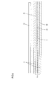
- FIG. 1 is a perspective view illustrating a schematic configuration of a liquid crystal display device of an embodiment in accordance with the present invention
- FIG. 2 is a sectional view of the liquid crystal display device of FIG. 1 taken on line A-A;
- FIG. 3 is a sectional view of a main part of a liquid crystal panel that the liquid crystal display device of FIG. 1 includes;
- FIG. 4 is an explanatory view illustrating an operational effect of the liquid crystal display device of the embodiment
- FIG. 5 is an explanatory view illustrating a lighting inspection step for an inspection-object liquid crystal panel.
- FIG. 6 is a side view illustrating a schematic configuration of a luminance point defect compensation device.
- FIGS. 1 through 6 An embodiment in accordance with the present invention will be described with reference to FIGS. 1 through 6 .
- FIG. 1 is a perspective view illustrating a schematic configuration of a liquid crystal display device of this embodiment
- FIG. 2 is a sectional view of the liquid crystal display device of FIG. 1 taken on line A-A
- FIG. 3 is a sectional view of a main part of a liquid crystal panel that the liquid crystal display device of FIG. 1 includes
- FIG. 4 is an explanatory view illustrating an operational effect that the liquid crystal display device of this embodiment produces
- FIG. 5 is an explanatory view illustrating a state of a lighting inspection step for an inspection-object liquid crystal panel
- FIG. 6 is a side view illustrating a schematic configuration of a luminance point defect compensating device.
- the liquid crystal display device 10 includes a liquid crystal panel 11 and a backlight device (a lighting device) 12 , which are integrally held by a bezel 13 etc.
- the liquid crystal panel 11 has a rectangular shape.
- the backlight device 12 is an external light source.
- the backlight device 12 is a backlight device of a so-called direct type.
- the backlight device 12 is sufficiently provided with a plurality of light sources (cold cathode tubes 17 are herein used as high-pressure discharge tubes) directly below the backside of a panel face (a display face) of the liquid crystal panel 11 and along the panel face.
- the liquid crystal panel 11 will be described below.
- the backlight device 12 includes a backlight chassis (chassis) 14 , a plurality of optical members 15 (a diffuser plate, a diffuser sheet, a lens sheet, and a reflection polarizing plate, which are in this order from below in the figure), and a frame 16 .
- the backlight chassis 14 has a substantial box shape with the top face side open.
- the optical members 15 are attached so as to cover the opening of the backlight chassis 14 .
- the frame 16 holds these optical members 15 over the backlight chassis 14 .
- the cold cathode tubes 17 , holders 18 made of rubber, lamp holders 19 , and lamp clips 20 are disposed in the backlight chassis 14 .
- the holders 18 hold both ends of the cold cathode tubes 17 .
- the lamp holders 19 collectively covers the cold cathode tubes 17 and the holders 18 .
- the lamp clips 20 are for the cold cathode tubes 17 to be attached to the backlight chassis 14 .
- the optical members 15 side from the LEDs 18 is a light emission side.
- Each cold cathode tube 17 has an elongated thin tubular shape.
- the plurality (16 tubes in FIG. 1 ) of cold cathode tubes 17 are accommodated in the backlight chassis 14 with the lengthwise direction (the axial direction) thereof parallel to the long side direction of the backlight chassis 14 .
- the lamp clips 20 which are for the cold cathode tubes 17 to be attached to the backlight chassis 14 , function as clip-shaped light source holders.
- the lamp clips 20 are made of synthetic resin (e.g. polycarbonate).
- the backlight chassis 14 has a light reflecting surface formed by a light reflecting sheet 14 a on the inner face side (the light source side) thereof.
- the backlight chassis 14 including the light reflecting sheet 14 a can reflect light, which is emitted from the cold cathode tubes 17 , to the optical members 15 (the diffuser plate etc.) side.
- the light reflecting sheet 14 a can be configured by, for example, a light-reflective resin sheet.
- the liquid crystal panel 11 has a configuration of a pair of substrates 30 , 40 and liquid crystal.
- the pair of substrates 30 , 40 are laminated together with a predetermined gap therebetween.
- the liquid crystal is sealed between the two substrates 30 , 40 and forms a liquid crystal layer 50 .
- the substrate 30 is an element substrate.
- the substrate 30 includes a glass substrate 31 , TFTs (thin-film transistors) 32 as semiconductor elements, pixel electrodes 33 , and an alignment film 34 .
- the TFTs 32 are formed on the liquid crystal layer 50 side of the glass substrate 31 .
- the pixel electrodes 33 are electrically connected to the TFTs 32 .
- the alignment film 34 is formed on the liquid crystal layer 50 side of the TFTs 32 and the pixel electrodes 33 .
- a polarizing plate 35 is laid on a side of the glass substrate 31 , the side being opposite from the liquid crystal layer 50 side. Note that, out of the pair of substrates 30 , 40 , the substrate 30 (the glass substrate 31 ) is disposed on the backlight device 12 side.
- the substrate 40 is an opposite substrate.
- the substrate 40 includes a glass substrate 41 , a color filter 42 , a counter electrode 43 , and an alignment film 44 .
- the color filter 42 is formed on the liquid crystal layer 50 side of the glass substrate 41 .
- the color filter 42 has color sections having respective colors of R (red), G (green), B (blue), etc. that are arrayed in a predetermined order.
- the counter electrode 43 is formed on the liquid crystal layer 50 side of the color filter 42 .
- the alignment film 44 is formed on the liquid crystal layer 50 side of the counter electrode 43 .
- a polarizing plate 45 is laid on a side of the glass substrate 41 , the side being opposite from the liquid crystal layer 50 side.
- a means for blocking light toward the foreign substance X is provided.
- a metal-halide containing region 60 is formed in a position in the glass substrate 31 of the substrate 30 and throughout the thickness direction of the glass substrate 31 , the position covering a projection of the foreign substance X in a planar view.
- the metal-halide containing region 60 contains silver chloride and silver bromide.
- silver chloride and silver bromide are substantially uniformly dispersed in a state deposited into microcrystals of approximately 10 nm in diameter. Silver chloride and silver bromide in such a state exhibit photochromism in the illumination light.
- the metal-halide containing region 60 when not irradiated with light, shows translucency similar to a usual glass substrate (see FIG. 3 ).
- the silver chloride and the silver bromide are photolyzed, and, accompanying this, silver atoms are generated.
- the silver atoms then form colloids, which blackens the metal-halide containing region 60 (see FIG. 4 ). Because the illumination light is blocked by this blackening, the emission light of the cold cathode tubes 17 does not reach the foreign substance X.
- the metal-halide containing region 60 is formed in the position in the glass substrate 31 , the metal-halide containing region 60 containing the metal halide which exhibits photochromism, the position being capable of blocking light toward the foreign substance (the luminance point defect occurrence portion) X that is a possible cause of the luminance point defect.
- This region is darkened upon supply of light from the cold cathode tubes 17 . This blocks the illumination light from the cold cathode tubes 17 , so that the illumination light does not reach the foreign substance X. Thus, higher display quality with the invisible luminance point defect can be realized.
- the metal-halide containing region 60 is formed throughout the thickness direction of the glass substrate 31 .
- the silver chloride and the silver bromide is contained in the glass substrate 31 , and this forms the metal-halide containing region 60 .
- the silver chloride and the silver bromide contained in the glass substrate 31 are blackened upon exhibition of photochromism in the emission light from the cold cathode tubes 17 . Therefore, light within a broader wavelength range can be blocked in the metal-halide containing region 60 , and the luminance point defect can still more certainly be invisible.
- the glass substrate 31 is provided, and the TFTs 32 and the pixel electrodes 33 are formed on the glass substrate 31 .
- the alignment film 34 is formed on the TFTs 32 and the pixel electrodes 33 .
- the substrate 30 which is the element substrate, is produced.
- the glass substrate 41 is provided, the color filter 42 is formed on the glass substrate, the counter electrode 43 is formed on the color filter 42 , and, further, the alignment film 44 is formed on the counter electrode 43 .
- the substrate 40 which is the opposite substrate, is produced.
- the substrate 30 and the substrate 40 are laminated together with a predetermined space therebetween, and liquid crystal is sealed in the space.
- the liquid crystal layer 50 is formed.
- the polarizing plates 35 , 45 are mounted on the respective faces of the two substrates 30 , 40 , the faces being opposite from the liquid crystal layer 50 side.
- the liquid crystal panel 11 is produced (see FIG. 3 ). Note that, in a below-described step of assembling the liquid crystal panel 11 and the backlight device 12 , the substrate 30 (the glass substrate 31 ) out of the two substrates 30 , 40 shall be disposed on the backlight device 12 side.
- an inspection-object liquid crystal panel 11 a the liquid crystal panel during the manufacturing progress of this case will hereinafter be referred to as an inspection-object liquid crystal panel 11 a ).
- a pair of polarizing plates 71 for inspection are arranged in a manner holding the substrates 30 , 40 of the inspection-object liquid crystal panel 11 a therebetween.
- the backlight 72 for inspection is lighted, while the wiring formed on the glass substrate 31 is connected to a circuit for inspection, and a signal is supplied to the wiring as required so that the TFTs 32 are driven.
- a display state which is obtained by thus controlling the oriented state of the liquid crystal configuring the liquid crystal layer, is inspected by image process or visually by the inspector.
- the luminance point defect which is viewed as a luminant point in spite that black is displayed.
- the cause of this luminance point defect can be that light strikes the foreign substance X that has entered the liquid crystal layer 50 and is diffusely reflected therefrom.
- the luminance point defect is compensated in a luminance point defect compensation step, which will be described below. Note that a conceivable cause of entrance of the foreign substance X into the liquid crystal layer 50 is that the foreign substance X has been clinging on the face on the liquid crystal layer 50 side of the substrates 30 , 40 , that the foreign substance X has been mixed in the liquid crystal, etc. at a stage before the liquid crystal is injected.
- the luminance point defect compensation step includes: a step of identifying the compensation position capable of blocking light toward the foreign substance X in the glass substrate 31 ; a step of doping the identified compensation position in the glass substrate 31 with halogen ions and metal ions; and irradiating the halogen ions and the metal ions in the doped compensation position with laser on the order of femtosecond or less so that crystals of metal halide which exhibits photochromism in the light supplied from the lighting device are deposited.
- the luminance point defect is compensated using a luminance point defect compensation device 70 illustrated in FIG. 6 .
- the luminance point defect compensation device 70 is configured by a stage 73 (not illustrated in FIG. 5 ), a pair of polarizing plates 71 for inspection, a backlight 72 for inspection, and an XYZ drive part 74 .
- the inspection-object liquid crystal panel 11 a which is the compensation object, is placed on the stage 73 .
- the pair of polarizing plates 71 for inspection are disposed in a manner holding the stage 73 therebetween.
- the XYZ drive part 74 moves parallel to and perpendicular to the stage 73 .
- the XYZ drive part 79 is provided with a CCD camera 75 , an ion implantation part 76 , and a laser irradiation part 77 , which are disposed in a predetermined positional relation.
- the CCD camera 75 is for imaging the foreign substance X and the portion surrounding the foreign substance X.
- the ion implantation part 76 is for implanting the halogenating ion and the metal ion.
- the laser irradiation part 77 is for laser irradiation for the crystals of the metal halide to be deposited.
- the stage 73 is made of glass to allow the light emitted from the backlight 72 for inspection to pass therethrough.
- the compensation position capable of blocking light toward the foreign substance X in the glass substrate 31 is identified.
- the inspection-object liquid crystal panel 11 a which is the compensation object, is placed in a predetermined position on the stage 73 with the glass substrate 31 upside.
- the backlight 72 is lighted, and the inspection-object liquid crystal panel 11 a is caused to display black.
- the display state is imaged using the CCD camera 75 while the XYZ drive part 74 is being moved parallel to the stage 73 , and the image result is image processed so that information on the position and the size of the foreign substance X is obtained.
- the position capable of blocking light toward the foreign substance X in the glass substrate 31 is identified.
- the identified position is doped with chloride ions, bromide ions, and silver ions.
- the doping with these ions shall be performed by an ion implantation method. Specifically, the XYZ drive part 74 is moved so that the ion implantation part 76 included therein is positioned right above the identified compensation position, and the ion doping are performed.
- the implanting conditions such as accelerating voltage is changed so that the doping is performed throughout the thickness direction of the glass substrate 31 .
- the ion-doped portion becomes a light-blocking layer in the end, which is a portion that is a possible black point in the display face. Therefore, the doping area in the direction of the face of the glass substrate 31 should be minimum. In this case, as a need arises, a means such as masking the surface of the glass substrate 31 (the top face of the inspection-object liquid crystal panel 11 a in FIG. 6 ) etc. should be adopted to the portion not to be doped.
- the process shifts to a step of depositing the crystals of the metal halide in the portion that has been ion-doped as described above.
- the crystals of the metal halide are deposited by irradiating the glass substrate 31 with the femtosecond laser having a pulse width on the order from 10 to 13 seconds.
- the XYZ drive part 74 is moved so that its laser irradiation part 77 is located right above the ion-doped portion, and laser irradiation is performed.
- the laser irradiation is performed under following conditions: the wavelength of 780 nm, the pulse width of 100 fs, the repetition frequency of 1 (one) kHz, the pulse energy of 1 (one) mJ, and the output of 1 (one) W.
- the chloride or bromide ions and the silver ions which exist in the focus point are activated by ablation effect and are bound together, so that crystals of silver halide and crystals of silver bromide are deposited.
- the region where silver chloride and silver bromide have been deposited can be formed as a continuous region along the path of the focus point.
- the metal-halide containing region 60 having the deposited crystals of silver chloride and silver bromide are formed throughout the thickness direction of the glass substrate 31 .
- the metal-halide containing region 60 formed as described above silver chloride and silver bromide are photolyzed upon irradiation with light, and the silver atoms, which are generated accompanying the photolyzation, form the colloids, and thus the metal-halide containing region 60 is blackened. Because this blackening blocks the illumination light, the light does not reach the foreign substance X (see FIG. 4 ).
- the liquid crystal display device 10 is produced.
- the liquid crystal display device 10 is obtained, the liquid crystal display device 10 being sufficiently provided with the metal-halide containing region 60 in the position in the glass substrate 31 , the metal-halide containing region 60 containing the crystals of the metal halide which is blackened upon supply of light from the backlight device 12 thereto, the position being capable of blocking light toward the foreign substance (the luminance point defect occurrence portion) X.
- the light supplied from the backlight device 12 is blocked by the blackened metal-halide containing region 60 and does not reach the foreign substance X.
- diffused reflection of light by the foreign substance X is not caused, so that the luminance point defect can be compensated so as to be invisible.
- the metal halide which exhibits photochromism is deposited so that the metal-halide containing region 60 is formed.
- the glass substrate is irradiated with the femtosecond laser, the energy is absorbed in the irradiated portion faster than the laser heat transfers to the portion surrounding the irradiation point. Therefore, the glass substrate surrounding the laser irradiation point is neither thermally nor chemically damaged. Thus, there is no concern for reducing the display quality of the liquid crystal display device 10 .
- the cold cathode tubes 17 are illustratively used as the light source.
- a light source that emits light within a wavelength range on the order from 10 nm to 100 nm may be sufficiently provided.
- Metal halide depending on its halogen ion species or metal ion species, has a characteristic wavelength range for exhibiting highly sensitive photochromism. Therefore, according to the used halogen ion species or metal ion species, a light source that emits light within the wavelength range for the ion species to exhibit photochromism may be selected. With this, the contained metal halide exhibits better photochromism, so that a higher light blocking effect can be produced.
- the metal-halide containing region 60 is formed in the position (an area) in the glass substrate 31 , the position covering the projection of the foreign substance X in a planar view.
- a metal-halide containing region having an area that is also capable of certainly blocking oblique incident illumination light should be formed.
- the metal-halide containing region may be formed in a manner entirely covering (i.e. blocking light toward) the pixel related to the portion where the foreign substance X has been mixed.
- the metal-halide containing region 60 is formed throughout the thickness direction of the glass substrate 31 .
- the thickness of the metal-halide containing region 60 is arbitrary.
- the position to form the metal-halide containing region 60 in the thickness direction of the glass substrate is arbitrary, e.g. the liquid crystal layer 50 side, the center in the thickness direction of the glass substrate, etc. Note however that, in order to certainly block the light, the metal-halide containing region 60 should be formed throughout the thickness direction.
- the crystals of silver chloride and the crystals of silver bromide are illustratively deposited as the metal halide. Also in a case where only one of silver chloride, silver bromide, and solid solution of silver chloride and silver bromide (AgCl ⁇ Br1- ⁇ ) is deposited, sufficient light blocking effect can be expected.
- the metal-halide containing region 60 is formed by irradiation with the femtosecond laser having the pulse width of 100 fs. From a standpoint of reducing damage to the portion surrounding the irradiation point, the pulse width should be smaller; laser having a pulse width still smaller but within the permissive range of the compensation performance may be used.
- the wavelength of the laser emitted to form the metal-halide containing region 60 is 780 nm. It is only necessary for the wavelength of the laser to be a wavelength for the laser to be less likely to be absorbed when passing through the glass substrate 31 ; the wavelength should be from 750 nm to 850 nm. Furthermore, also the other conditions of irradiation may be modified depending on the composition of the irradiation-object glass substrate.
- the step of identifying the compensation position, the step of doping with kinds of ions, and the step of depositing the metal halide by irradiation with laser are performed using the luminance point defect compensation device 70 .
- separate devices may be provided to perform respective steps.
- the luminance point defect compensation device 70 has a configuration of the XYZ drive part 74 that includes the CCD camera 75 , the ion implantation part 76 , and the laser irradiation part 77 and moves parallel to and perpendicular to the stage 73 . It may be configured such that the CCD camera, the ion implantation part, and the laser irradiation part are fixed while the stage moves parallel to and perpendicular to the CCD camera and the laser irradiation part.
- the luminance point defect is due to the foreign substance X that has entered the inside of the liquid crystal layer 50 .
- the TFTs 32 and the pixel electrodes 33 etc. can cause misoperation due to a short circuit etc., and this can be the cause of the luminance point defect.
- the present invention is adoptable also to such a case.
- the present invention may be adopted to a liquid crystal display device that uses an switching element other than the TFTs 32 .
Landscapes
- Physics & Mathematics (AREA)
- Nonlinear Science (AREA)
- Chemical & Material Sciences (AREA)
- Crystallography & Structural Chemistry (AREA)
- General Physics & Mathematics (AREA)
- Optics & Photonics (AREA)
- Mathematical Physics (AREA)
- Devices For Indicating Variable Information By Combining Individual Elements (AREA)
- Liquid Crystal (AREA)
Abstract
Description
Claims (8)
Applications Claiming Priority (3)
| Application Number | Priority Date | Filing Date | Title |
|---|---|---|---|
| JP2007-192047 | 2007-07-24 | ||
| JP2007192047 | 2007-07-24 | ||
| PCT/JP2008/056574 WO2009013921A1 (en) | 2007-07-24 | 2008-04-02 | Liquid crystal display device and its manufacturing method |
Publications (2)
| Publication Number | Publication Date |
|---|---|
| US20100201912A1 US20100201912A1 (en) | 2010-08-12 |
| US8072559B2 true US8072559B2 (en) | 2011-12-06 |
Family
ID=40281181
Family Applications (1)
| Application Number | Title | Priority Date | Filing Date |
|---|---|---|---|
| US12/668,853 Expired - Fee Related US8072559B2 (en) | 2007-07-24 | 2008-04-02 | Liquid crystal display device and manufacturing method thereof |
Country Status (3)
| Country | Link |
|---|---|
| US (1) | US8072559B2 (en) |
| CN (1) | CN101743502B (en) |
| WO (1) | WO2009013921A1 (en) |
Cited By (1)
| Publication number | Priority date | Publication date | Assignee | Title |
|---|---|---|---|---|
| US20130021466A1 (en) * | 2011-07-21 | 2013-01-24 | Photon Dynamics, Inc. | Apparatus for viewing through optical thin film color filters and their overlaps |
Families Citing this family (5)
| Publication number | Priority date | Publication date | Assignee | Title |
|---|---|---|---|---|
| KR102094427B1 (en) * | 2013-08-07 | 2020-03-30 | 삼성디스플레이 주식회사 | Organic light emitting diode display |
| JP6362013B2 (en) * | 2016-12-28 | 2018-07-25 | パナソニックIpマネジメント株式会社 | Display device, manufacturing method thereof, and manufacturing apparatus |
| US20200124928A1 (en) * | 2017-03-09 | 2020-04-23 | Sakai Display Products Corporation | Method for correcting defect, defect correction apparatus, and display panel |
| CN107422528A (en) * | 2017-07-28 | 2017-12-01 | 京东方科技集团股份有限公司 | A kind of blooming piece, backlight module and display device |
| CN109597247B (en) * | 2019-02-19 | 2022-04-29 | 京东方科技集团股份有限公司 | Display panel, backlight source and correction device thereof |
Citations (10)
| Publication number | Priority date | Publication date | Assignee | Title |
|---|---|---|---|---|
| JPH04301617A (en) | 1991-03-29 | 1992-10-26 | Sharp Corp | Liquid crystal display device and method for repairing defects in liquid crystal display device |
| US5280374A (en) | 1991-03-01 | 1994-01-18 | Sharp Kabushiki Kaisha | Liquid crystal display device and method of compensating for a defect |
| JPH06308442A (en) | 1993-04-27 | 1994-11-04 | Sanyo Electric Co Ltd | Method for correcting dot defect |
| JPH09311350A (en) | 1996-05-23 | 1997-12-02 | Sony Corp | Liquid crystal display element defect repairing apparatus and defect repairing method |
| US5756649A (en) * | 1994-05-17 | 1998-05-26 | Japan Synthetic Rubber Co., Ltd. | Liquid crystal aligning agent and liquid crystal display device |
| JPH10333186A (en) | 1997-05-28 | 1998-12-18 | Casio Comput Co Ltd | Liquid crystal display |
| US20040179028A1 (en) | 2003-03-12 | 2004-09-16 | Fuji Photo Film Co., Ltd. | Pixel defect correcting method, color mura correcting method and image display device |
| JP2004279464A (en) | 2003-03-12 | 2004-10-07 | Fuji Photo Film Co Ltd | Method for correcting pixel defect and image display device |
| US20090207353A1 (en) * | 2008-02-19 | 2009-08-20 | Fujifilm Corporation | Substrate for liquid crystal display device and liquid crystal display device |
| US20100277684A1 (en) * | 2007-10-22 | 2010-11-04 | Hiroshi Fukushima | Display device and method for production thereof |
-
2008
- 2008-04-02 WO PCT/JP2008/056574 patent/WO2009013921A1/en not_active Ceased
- 2008-04-02 US US12/668,853 patent/US8072559B2/en not_active Expired - Fee Related
- 2008-04-02 CN CN2008800247242A patent/CN101743502B/en not_active Expired - Fee Related
Patent Citations (10)
| Publication number | Priority date | Publication date | Assignee | Title |
|---|---|---|---|---|
| US5280374A (en) | 1991-03-01 | 1994-01-18 | Sharp Kabushiki Kaisha | Liquid crystal display device and method of compensating for a defect |
| JPH04301617A (en) | 1991-03-29 | 1992-10-26 | Sharp Corp | Liquid crystal display device and method for repairing defects in liquid crystal display device |
| JPH06308442A (en) | 1993-04-27 | 1994-11-04 | Sanyo Electric Co Ltd | Method for correcting dot defect |
| US5756649A (en) * | 1994-05-17 | 1998-05-26 | Japan Synthetic Rubber Co., Ltd. | Liquid crystal aligning agent and liquid crystal display device |
| JPH09311350A (en) | 1996-05-23 | 1997-12-02 | Sony Corp | Liquid crystal display element defect repairing apparatus and defect repairing method |
| JPH10333186A (en) | 1997-05-28 | 1998-12-18 | Casio Comput Co Ltd | Liquid crystal display |
| US20040179028A1 (en) | 2003-03-12 | 2004-09-16 | Fuji Photo Film Co., Ltd. | Pixel defect correcting method, color mura correcting method and image display device |
| JP2004279464A (en) | 2003-03-12 | 2004-10-07 | Fuji Photo Film Co Ltd | Method for correcting pixel defect and image display device |
| US20100277684A1 (en) * | 2007-10-22 | 2010-11-04 | Hiroshi Fukushima | Display device and method for production thereof |
| US20090207353A1 (en) * | 2008-02-19 | 2009-08-20 | Fujifilm Corporation | Substrate for liquid crystal display device and liquid crystal display device |
Non-Patent Citations (1)
| Title |
|---|
| Chinese Office Action, The State Intellectual Property Office of the People's Republic of China, Mar. 2, 2011. |
Cited By (2)
| Publication number | Priority date | Publication date | Assignee | Title |
|---|---|---|---|---|
| US20130021466A1 (en) * | 2011-07-21 | 2013-01-24 | Photon Dynamics, Inc. | Apparatus for viewing through optical thin film color filters and their overlaps |
| US9535273B2 (en) * | 2011-07-21 | 2017-01-03 | Photon Dynamics, Inc. | Apparatus for viewing through optical thin film color filters and their overlaps |
Also Published As
| Publication number | Publication date |
|---|---|
| WO2009013921A1 (en) | 2009-01-29 |
| CN101743502A (en) | 2010-06-16 |
| US20100201912A1 (en) | 2010-08-12 |
| CN101743502B (en) | 2012-03-14 |
Similar Documents
| Publication | Publication Date | Title |
|---|---|---|
| CN101772725B (en) | Liquid crystal display and method for manufacturing the same | |
| TWI386717B (en) | Liquid crystal display apparatus and liquid crystal panel | |
| CN101765801B (en) | Liquid crystal display device and manufacturing method thereof | |
| US8072559B2 (en) | Liquid crystal display device and manufacturing method thereof | |
| US8233112B2 (en) | Liquid crystal display apparatus and manufacturing method thereof | |
| JP5117502B2 (en) | Manufacturing method of liquid crystal display device | |
| CN101772724B (en) | Liquid crystal display device and method of manufacturing same | |
| TW201222067A (en) | Liquid crystal panel, method for manufacturing same, liquid crystal display device and television receiving device | |
| US8054389B2 (en) | Liquid crystal display apparatus having particular optical compensation layers | |
| JPH08146370A (en) | Liquid crystal display defect correction method | |
| KR100608890B1 (en) | Liquid crystal display panel and liquid crystal display device having same | |
| JP3664309B2 (en) | Projection type liquid crystal display device | |
| JPH08248367A (en) | Liquid crystal display device manufacturing method and liquid crystal display device | |
| GB2439352A (en) | Adjusting amount of liquid crystal in liquid crystal display device | |
| JP2008151919A (en) | Reflective liquid crystal display element | |
| JPH04147182A (en) | Projection type liquid crystal display device | |
| JPH04353821A (en) | Liquid crystal display device and its defect correcting method | |
| JP2004070082A (en) | Liquid crystal display element and liquid crystal display device |
Legal Events
| Date | Code | Title | Description |
|---|---|---|---|
| AS | Assignment |
Owner name: SHARP KABUSHIKI KAISHA, JAPAN Free format text: ASSIGNMENT OF ASSIGNORS INTEREST;ASSIGNOR:IKEDA, MASAKI;REEL/FRAME:023833/0073 Effective date: 20091202 |
|
| ZAAA | Notice of allowance and fees due |
Free format text: ORIGINAL CODE: NOA |
|
| ZAAB | Notice of allowance mailed |
Free format text: ORIGINAL CODE: MN/=. |
|
| STCF | Information on status: patent grant |
Free format text: PATENTED CASE |
|
| FEPP | Fee payment procedure |
Free format text: PAYOR NUMBER ASSIGNED (ORIGINAL EVENT CODE: ASPN); ENTITY STATUS OF PATENT OWNER: LARGE ENTITY |
|
| FEPP | Fee payment procedure |
Free format text: PAYER NUMBER DE-ASSIGNED (ORIGINAL EVENT CODE: RMPN); ENTITY STATUS OF PATENT OWNER: LARGE ENTITY Free format text: PAYOR NUMBER ASSIGNED (ORIGINAL EVENT CODE: ASPN); ENTITY STATUS OF PATENT OWNER: LARGE ENTITY |
|
| FPAY | Fee payment |
Year of fee payment: 4 |
|
| MAFP | Maintenance fee payment |
Free format text: PAYMENT OF MAINTENANCE FEE, 8TH YEAR, LARGE ENTITY (ORIGINAL EVENT CODE: M1552); ENTITY STATUS OF PATENT OWNER: LARGE ENTITY Year of fee payment: 8 |
|
| FEPP | Fee payment procedure |
Free format text: MAINTENANCE FEE REMINDER MAILED (ORIGINAL EVENT CODE: REM.); ENTITY STATUS OF PATENT OWNER: LARGE ENTITY |
|
| LAPS | Lapse for failure to pay maintenance fees |
Free format text: PATENT EXPIRED FOR FAILURE TO PAY MAINTENANCE FEES (ORIGINAL EVENT CODE: EXP.); ENTITY STATUS OF PATENT OWNER: LARGE ENTITY |
|
| STCH | Information on status: patent discontinuation |
Free format text: PATENT EXPIRED DUE TO NONPAYMENT OF MAINTENANCE FEES UNDER 37 CFR 1.362 |
|
| FP | Lapsed due to failure to pay maintenance fee |
Effective date: 20231206 |