US8072263B2 - Power control device for a signal with optimized input dynamics - Google Patents
Power control device for a signal with optimized input dynamics Download PDFInfo
- Publication number
- US8072263B2 US8072263B2 US12/640,332 US64033209A US8072263B2 US 8072263 B2 US8072263 B2 US 8072263B2 US 64033209 A US64033209 A US 64033209A US 8072263 B2 US8072263 B2 US 8072263B2
- Authority
- US
- United States
- Prior art keywords
- amplification channel
- amplifier
- gain
- current
- control device
- Prior art date
- Legal status (The legal status is an assumption and is not a legal conclusion. Google has not performed a legal analysis and makes no representation as to the accuracy of the status listed.)
- Expired - Fee Related
Links
- 230000003321 amplification Effects 0.000 claims abstract description 51
- 238000003199 nucleic acid amplification method Methods 0.000 claims abstract description 51
- 230000010287 polarization Effects 0.000 claims description 20
- 238000000034 method Methods 0.000 claims description 4
- 230000000750 progressive effect Effects 0.000 claims description 4
- 230000001419 dependent effect Effects 0.000 claims description 3
- 238000007493 shaping process Methods 0.000 claims description 2
- 230000005540 biological transmission Effects 0.000 description 4
- 230000006835 compression Effects 0.000 description 4
- 238000007906 compression Methods 0.000 description 4
- 230000002411 adverse Effects 0.000 description 2
- 238000004458 analytical method Methods 0.000 description 1
- 230000000712 assembly Effects 0.000 description 1
- 238000000429 assembly Methods 0.000 description 1
- 230000000694 effects Effects 0.000 description 1
- 230000010354 integration Effects 0.000 description 1
- 230000035945 sensitivity Effects 0.000 description 1
Images


Classifications
-
- H—ELECTRICITY
- H03—ELECTRONIC CIRCUITRY
- H03G—CONTROL OF AMPLIFICATION
- H03G1/00—Details of arrangements for controlling amplification
- H03G1/0005—Circuits characterised by the type of controlling devices operated by a controlling current or voltage signal
- H03G1/0035—Circuits characterised by the type of controlling devices operated by a controlling current or voltage signal using continuously variable impedance elements
Definitions
- the present invention relates to a power control device for a signal with optimized input dynamics.
- the device according to the invention enables automatic gain control of the power control device. It is applied, for example, to the signal reception channel in a satellite geopositioning device.
- An automatic gain control device notably used in a radio transmission or reception channel, enables adjustment of the amplification gain of the input signal in such a way as to obtain an acceptable signal level at the channel output, independently of the power of the input signal. This enables presentation to the circuit located at the end of the transmission or reception channel of a signal whose power is optimum for guaranteeing the expected performance of the transmission/reception channel.
- Devices such as, for example, channels for the reception of signals originating from satellites, which are fitted to geopositioning devices such as GPS (“Global Positioning System”) receivers, operate under high input dynamics, with extremely low-power signals. It must be noted here that signals with high input dynamics are signals in which the difference between the highest levels and the lowest levels is great. In devices of this type, it is necessary to minimize the interference caused by any non-linearity of the system in order to be able to ensure acceptable sensitivity. The system therefore requires a function whose performance is constant across the entire input dynamic range. Moreover, for applications with very low consumption, it is necessary to ensure that the automatic gain control minimizes consumption.
- the present invention overcomes the aforementioned problems by proposing a solution which provides a guarantee of the required performance for low-power signals, while minimizing consumption in the case of higher-power signals.
- the invention guarantees the required compression level in relation to the processed signal, for example by maintaining a level of 10 dB above the nominal processed signal across the entire dynamic range of the input signal.
- the invention consists in switching in a progressive manner two parallel amplification channels whose characteristics are distinct and whose gain is current-controlled in order to guarantee both the expected gain dynamics and a compression level which is consistent with the processed signal.
- a current law is implemented in order to distribute the gains of the two channels in an optimum manner.
- a first amplification channel comprises a first amplifier
- a second amplification channel comprises a passive attenuator in series with a second amplifier.
- the output signal is obtained by adding together the output signals of the two parallel structures.
- a further advantage of this invention is to enable integration of the power control device into integrated circuits implemented according to the known techniques of Monolithic Microwave Integrated Circuits (MMICs), or Application-Specific Integrated Circuits (ASICs).
- MMICs Monolithic Microwave Integrated Circuits
- ASICs Application-Specific Integrated Circuits
- the subject of the invention is a signal power control device comprising a first amplification channel comprising a first amplifier, a second amplification channel comprising a fixed-gain attenuator in series with a second amplifier, and an adder, the first amplification channel and the second amplification channel comprising gain adjustment means, an input signal being applied to the first amplification channel, and in parallel with the second amplification channel, the outputs of the first and second amplification channels being connected to the inputs of the adder, the gain adjustment means being suitable for distributing the respective gains of the first amplification channel and the second amplification channel depending on the power of the input signal according to a distribution law according to which the gain of the second amplification channel is minimal for the lowest input powers, and the gain of the first amplifier channel is minimal for the highest input powers, the gains of the first amplification channel and the second amplification channel being adjusted in a progressive and continuous manner for the intermediate input powers.
- the signal power control device described above can be characterized in that the first amplifier and the second amplifier are transconductance amplifiers, the gain adjustment means comprising means for controlling a first polarization current I 1 of the first amplifier, and a second polarization current I 2 of the second amplifier depending on a control current I c .
- the power control device can be characterized in that the gain of the control device expressed in decibels is proportional to the logarithm of the control current I c in the normal operating range.
- the signal power control device described above can be characterized in that the means for controlling the first polarization current I 1 of the first amplifier and the second current I 2 are suitable for shaping the two currents, each according to a law dependent on a control current I c .
- a further subject of the invention is a satellite geopositioning device comprising a signal reception and amplification channel, comprising a power control device as described above.
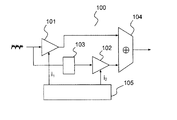
- FIG. 1 shows the synopsis of an example of a power control device according to the invention
- FIG. 2 shows the synopsis of an example of the structure of the current control device according to the invention
- FIG. 3 a shows an example of graphs representing the polarization currents of the two amplifiers, depending on a control current
- FIG. 3 b shows an example of a graph representing the gain of the power control device according to the invention, depending on the control current
- FIG. 3 c shows an example of a graph representing the dynamics of the input signal of the power control device according to the invention, depending on the control current.
- FIG. 1 shows, in synoptic form, an example of a power control device 100 according to the invention.
- the device 100 comprises a first amplifier 101 , a second amplifier 102 , an attenuator 103 , an adder 104 and a device 105 to control the polarization currents of the amplifiers 101 and 102 .
- the polarization currents of the amplifiers 101 and 102 are hereafter respectively denoted as I 1 and I 2 .
- An input signal is sent on a first amplification channel comprising exclusively the first amplifier 101 , and in parallel on a second amplification channel, comprising the attenuator 103 , which is mounted in series with the amplifier 102 .
- the output signals of these two amplification channels are summated by the adder 104 , from which the output signal of the power control device originates.
- the amplifiers 101 and 102 are transconductance amplifiers whose gain can be controlled by their polarization current.
- the two amplifiers 101 and 102 may, for example, present identical structural characteristics.
- the current control device 105 is powered by a current source not shown in the Figure, but described below with reference to FIG. 2 . If the power control device according to the invention is used in a satellite geopositioning receiver, the signal applied to the input of the power device 100 may, for example, originate from an integrated antenna or an active external antenna, i.e. producing an amplified signal. In both cases, the useful signal presents low dynamics in relation to the noise, but the amplitude of the input signal may nevertheless vary within a wide range of values, up to a value in the order of several hundred millivolts peak-to-peak.
- the invention proposes that a single power control channel, which can be easily integrated within a printed circuit, can process both high-amplitude signals and low-amplitude signals in an optimum manner, i.e. it enables the presentation, to a circuit located at the end of the transmission or reception channel, of a signal guaranteeing the expected system performance.
- the power control device must be capable of supplying ideally constant output dynamics, over the widest possible gain range, typically in the order of 30 dB.
- the amplifiers 101 and 102 each comprise, for example, a transistor.
- the power control device 100 thus comprises a stack of two transistors, in contrast to automatic gain control devices known in the state of the art, which normally comprise three amplifiers, typically transistors, in cascode assemblies.
- the power control device 100 may therefore merely require a low-voltage power supply, typically two third of the power supply voltage required by a known device based on a cascode assembly.
- the current control device 105 enables the adjustment of the respective gains of the two amplifiers 101 and 102 in an independent manner, the total gain of the power control device being the sum of the gains of the two amplifiers 101 and 102 and the attenuator 103 .
- the law imposed on the polarization currents of each of the two amplifiers 101 and 102 , as well as the characteristics of the attenuator 103 , whose attenuation factor is fixed, are calculated in such a way as to guarantee more or less constant output dynamics over the chosen gain range.
- the polarization current I 1 of the first amplifier 101 is reduced according to a first law determined and described more precisely with reference to FIG. 3 , whereas the polarization current I 2 of the second amplifier increases according to a determined second law, thereby enabling an increase in the input dynamics thanks to the presence of the attenuator 103 .
- the current I 2 is at its maximum value, whereas the current I 1 is zero.
- the value of the attenuation factor of the attenuator 103 allows the input dynamics of the power control device 100 to be increased and the maximum gain of this value to be reduced.
- FIG. 2 shows the synopsis of an example of the structure of the current control device 105 according to the invention.
- the current control device 105 comprises a first block 201 to generate the polarization current of the first amplifier 101 , and a second block 202 to generate the polarization current I 2 of the second amplifier 102 .
- a third current-generating block 203 produces a first reference current I ref .
- a fourth current-generating block 204 produces a second reference current ⁇ I ref , where ⁇ is a coefficient defining the useful gain dynamics of the power control device; the value of ⁇ is determined by the attenuation coefficient of the attenuator 103 .
- a single current source may, for example, be used to generate the two reference currents I ref and ⁇ I ref .
- the first block 201 for generating the current and the second block 202 for generating the current I 2 are controlled by the command current I c , and also by the command currents I ref and ⁇ I ref .
- Each of the currents and I 2 complies with a law dependent on the control current I c , and also the reference currents I ref and ⁇ I ref .
- control current I c follows a law proportional to the absolute temperature, known to the person skilled in the art by the name of PTAT (Proportional To Absolute Temperature).
- reference currents I ref and ⁇ I ref are proportional to the absolute temperature.
- FIG. 3 a shows an example of graphs 301 and 302 respectively representing the polarization currents and I 2 of the two amplifiers 101 and 102 , depending on the control current I c represented according to a logarithmic scale.
- FIG. 3 b shows an example of a graph representing the gain of the power control device according to the invention, depending on the control current I c , represented according to a logarithmic scale.
- FIG. 3 c shows an example of a graph representing the dynamics of the input signal of the power control device according to the invention, expressed as mV pp , depending on the control current I c .
- a parallel analysis of FIGS. 3 a , 3 b and 3 c enables a better understanding of the invention.
- the reference current I ref is set to 80 ⁇ A and the current ⁇ I ref to 15 ⁇ A. It must be noted that these two reference currents define the useful gain dynamics.
- the current I 1 is at a maximum value of 316 ⁇ A, whereas the current I 2 is zero. If the gain needs to be reduced in the required gain dynamics, with a slope of 40 dB per decade in the example shown in FIG.
- the control current I c reduces; the current I i begins to reduce progressively, and the current I 2 begins to increase.
- the minimum gain value in the required gain dynamics in the order of ⁇ 12 dB in the example shown in FIG. 3 b , for input dynamics in the order of 600 mV pp in the example shown in FIG. 3 c , corresponds to a control current I c value equal to the reference current ⁇ I ref .
- the power control device 100 produces a low gain margin, in which the gain may reduce with the current rather than remain fixed at a minimum value, and also a high gain margin, in which the gain can increase with the current.
- the gain may vary depending on the control current I c by 20 dB per decade.
- the input dynamics remain stable in the low and high gain margins, the current I 1 being zero in the low margin, and the current I 2 in the high margin.
- the gain control law is perfectly linear in the normal operating range, i.e. the gain in dB is linear depending on the control current I c expressed on a logarithmic scale.
- the normal operating range is, in other words, the optimized operating range in terms of the input dynamics.
- the linearity offers an advantage for the calculation of the control current which is to be applied, and also for the calculation of the loop and for its stability. More precisely, in the normal operating range, the two amplification blocks formed by the amplifiers 101 and 102 are active, their respective polarization currents I 1 and I 2 being non-zero; the slope in the example shown in FIG. 3 b being 40 dB per decade, thanks to the laws for the applied currents I 1 and I 2 .
Landscapes
- Amplifiers (AREA)
Abstract
Description
Claims (7)
Applications Claiming Priority (2)
| Application Number | Priority Date | Filing Date | Title |
|---|---|---|---|
| FR0807236 | 2008-12-19 | ||
| FR0807236A FR2940554B1 (en) | 2008-12-19 | 2008-12-19 | DEVICE FOR CONTROLLING THE POWER OF A SIGNAL WITH OPTIMIZED ENTRY DYNAMIC |
Publications (2)
| Publication Number | Publication Date |
|---|---|
| US20100156719A1 US20100156719A1 (en) | 2010-06-24 |
| US8072263B2 true US8072263B2 (en) | 2011-12-06 |
Family
ID=40854611
Family Applications (1)
| Application Number | Title | Priority Date | Filing Date |
|---|---|---|---|
| US12/640,332 Expired - Fee Related US8072263B2 (en) | 2008-12-19 | 2009-12-17 | Power control device for a signal with optimized input dynamics |
Country Status (2)
| Country | Link |
|---|---|
| US (1) | US8072263B2 (en) |
| FR (1) | FR2940554B1 (en) |
Citations (5)
| Publication number | Priority date | Publication date | Assignee | Title |
|---|---|---|---|---|
| EP1524769A2 (en) | 2003-10-09 | 2005-04-20 | Sharp Kabushiki Kaisha | Current switch circuit, amplifier, and mobile terminal |
| GB2432735A (en) | 2005-11-28 | 2007-05-30 | Via Tech Inc | Extended range dB-linear variable gain RF amplifier |
| US7250814B2 (en) * | 2004-04-03 | 2007-07-31 | International Business Machines Corporation | Variable gain amplifier |
| US20070296501A1 (en) | 2006-06-12 | 2007-12-27 | Nec Electronics Corporation | Variable-gain amplifier |
| US20080186100A1 (en) | 2007-02-05 | 2008-08-07 | Sony Corporation | Variable-gain amplification circuit, receiver and receiver ic |
-
2008
- 2008-12-19 FR FR0807236A patent/FR2940554B1/en not_active Expired - Fee Related
-
2009
- 2009-12-17 US US12/640,332 patent/US8072263B2/en not_active Expired - Fee Related
Patent Citations (5)
| Publication number | Priority date | Publication date | Assignee | Title |
|---|---|---|---|---|
| EP1524769A2 (en) | 2003-10-09 | 2005-04-20 | Sharp Kabushiki Kaisha | Current switch circuit, amplifier, and mobile terminal |
| US7250814B2 (en) * | 2004-04-03 | 2007-07-31 | International Business Machines Corporation | Variable gain amplifier |
| GB2432735A (en) | 2005-11-28 | 2007-05-30 | Via Tech Inc | Extended range dB-linear variable gain RF amplifier |
| US20070296501A1 (en) | 2006-06-12 | 2007-12-27 | Nec Electronics Corporation | Variable-gain amplifier |
| US20080186100A1 (en) | 2007-02-05 | 2008-08-07 | Sony Corporation | Variable-gain amplification circuit, receiver and receiver ic |
Also Published As
| Publication number | Publication date |
|---|---|
| FR2940554A1 (en) | 2010-06-25 |
| US20100156719A1 (en) | 2010-06-24 |
| FR2940554B1 (en) | 2013-07-05 |
Similar Documents
| Publication | Publication Date | Title |
|---|---|---|
| US5886575A (en) | Apparatus and method for amplifying a signal | |
| RU2434317C2 (en) | Radio-frequency power amplifiers | |
| US6492874B1 (en) | Active bias circuit | |
| US6885246B2 (en) | High frequency amplifier | |
| KR960016642B1 (en) | Transceiver | |
| US8791760B2 (en) | Closed loop bias control | |
| US7446609B2 (en) | Variable gain amplifier with gain adjusting circuit | |
| US6753732B1 (en) | Accurate, wide-band, low-noise variable-gain amplifier structures and gain control methods | |
| US7701288B2 (en) | Variable gain amplifiers | |
| US7825730B2 (en) | Bias circuit for the wireless transceiver | |
| JP4029086B2 (en) | Transmitting device and portable communication terminal device | |
| KR20090087990A (en) | 수신기 Receiver with current regulator to reduce power consumption through optimization | |
| EP3425796B1 (en) | Amplifier | |
| US8072263B2 (en) | Power control device for a signal with optimized input dynamics | |
| WO2019085830A1 (en) | Hybrid variable gain amplifier | |
| US8179198B2 (en) | Variable gain amplifier having automatic power consumption optimization | |
| Min et al. | Ka-band CMOS variable-gain amplifier using capacitive compensation technique to suppress phase error | |
| US6710647B1 (en) | Method and circuit for distortion compensation and output control | |
| JP2009534957A (en) | Temperature compensated CMOS transmitter circuit with merged mixer and variable gain amplifier | |
| US7565118B2 (en) | Polar modulation transmission apparatus and wireless communication apparatus | |
| US20120286860A1 (en) | Systems and Methods for Minimizing Phase Deviation and/or Amplitude Modulation (AM)-to-Phase Modulation (PM) Conversion for Dynamic Range, Radio Frequency (RF) Non-Linear Amplifiers | |
| US6750713B1 (en) | Variable gain amplifier | |
| US9136797B2 (en) | Adaptive harmonic distortion suppression in an amplifier utilizing negative gain | |
| US10637422B1 (en) | Gain compensation for an open loop programmable amplifier for high speed applications | |
| EP1429456A1 (en) | Variable gain amplifier of low power consumption |
Legal Events
| Date | Code | Title | Description |
|---|---|---|---|
| AS | Assignment |
Owner name: THALES,FRANCE Free format text: ASSIGNMENT OF ASSIGNORS INTEREST;ASSIGNORS:LOUIS, BRUNO;PETIT, VINCENT;CORBIERE, REMI;REEL/FRAME:023835/0103 Effective date: 20100118 Owner name: THALES, FRANCE Free format text: ASSIGNMENT OF ASSIGNORS INTEREST;ASSIGNORS:LOUIS, BRUNO;PETIT, VINCENT;CORBIERE, REMI;REEL/FRAME:023835/0103 Effective date: 20100118 |
|
| STCF | Information on status: patent grant |
Free format text: PATENTED CASE |
|
| CC | Certificate of correction | ||
| FPAY | Fee payment |
Year of fee payment: 4 |
|
| FEPP | Fee payment procedure |
Free format text: MAINTENANCE FEE REMINDER MAILED (ORIGINAL EVENT CODE: REM.); ENTITY STATUS OF PATENT OWNER: LARGE ENTITY |
|
| LAPS | Lapse for failure to pay maintenance fees |
Free format text: PATENT EXPIRED FOR FAILURE TO PAY MAINTENANCE FEES (ORIGINAL EVENT CODE: EXP.); ENTITY STATUS OF PATENT OWNER: LARGE ENTITY |
|
| STCH | Information on status: patent discontinuation |
Free format text: PATENT EXPIRED DUE TO NONPAYMENT OF MAINTENANCE FEES UNDER 37 CFR 1.362 |
|
| FP | Lapsed due to failure to pay maintenance fee |
Effective date: 20191206 |