US8072159B2 - Multi-lamp driving circuit - Google Patents
Multi-lamp driving circuit Download PDFInfo
- Publication number
- US8072159B2 US8072159B2 US12/416,163 US41616309A US8072159B2 US 8072159 B2 US8072159 B2 US 8072159B2 US 41616309 A US41616309 A US 41616309A US 8072159 B2 US8072159 B2 US 8072159B2
- Authority
- US
- United States
- Prior art keywords
- circuit
- transformer
- output end
- power stage
- balancing
- Prior art date
- Legal status (The legal status is an assumption and is not a legal conclusion. Google has not performed a legal analysis and makes no representation as to the accuracy of the status listed.)
- Expired - Fee Related, expires
Links
- 239000003990 capacitor Substances 0.000 claims abstract description 40
- 238000004804 winding Methods 0.000 claims description 35
- 238000010586 diagram Methods 0.000 description 14
- 238000000034 method Methods 0.000 description 1
Images


Classifications
-
- H—ELECTRICITY
- H05—ELECTRIC TECHNIQUES NOT OTHERWISE PROVIDED FOR
- H05B—ELECTRIC HEATING; ELECTRIC LIGHT SOURCES NOT OTHERWISE PROVIDED FOR; CIRCUIT ARRANGEMENTS FOR ELECTRIC LIGHT SOURCES, IN GENERAL
- H05B41/00—Circuit arrangements or apparatus for igniting or operating discharge lamps
- H05B41/14—Circuit arrangements
- H05B41/26—Circuit arrangements in which the lamp is fed by power derived from dc by means of a converter, e.g. by high-voltage dc
- H05B41/28—Circuit arrangements in which the lamp is fed by power derived from dc by means of a converter, e.g. by high-voltage dc using static converters
- H05B41/282—Circuit arrangements in which the lamp is fed by power derived from dc by means of a converter, e.g. by high-voltage dc using static converters with semiconductor devices
- H05B41/2825—Circuit arrangements in which the lamp is fed by power derived from dc by means of a converter, e.g. by high-voltage dc using static converters with semiconductor devices by means of a bridge converter in the final stage
- H05B41/2827—Circuit arrangements in which the lamp is fed by power derived from dc by means of a converter, e.g. by high-voltage dc using static converters with semiconductor devices by means of a bridge converter in the final stage using specially adapted components in the load circuit, e.g. feed-back transformers, piezoelectric transformers; using specially adapted load circuit configurations
Definitions
- Embodiments of the present disclosure relate to lamp driving circuits, and particularly to a multi-lamp driving circuit.
- discharge lamps such as Cold Cathode Fluorescent Lamps (CCFLs) and External Electrode Fluorescent Lamps (EEFLs)
- CCFLs Cold Cathode Fluorescent Lamps
- EFLs External Electrode Fluorescent Lamps
- Balancing circuits often only utilize capacitors or transformers connected to the discharge lamps. Balancing circuits utilizing only capacitors provide a simple and cost-effective solution, but overall balancing effects suffer. Balancing circuits using only transformers provide better balancing effects, but at a cost increase.
- FIG. 1 is a circuit diagram of a balancing circuit for a multi-lamp driving circuit in accordance with the present disclosure
- FIG. 2 a is a schematic diagram of a first embodiment of a multi-lamp driving circuit using the balancing circuit of FIG. 1 ;
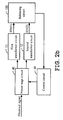
- FIG. 2 b is a schematic diagram of a second embodiment of a multi-lamp driving circuit using the balancing circuit of FIG. 1 ;
- FIG. 2 c is a schematic diagram of a third embodiment of a multi-lamp driving circuit using the balancing circuit of FIG. 1 ;
- FIG. 3 is a circuit diagram of another balancing circuit for a multi-lamp driving circuit in accordance with the present disclosure
- FIG. 4 a is a schematic diagram of a first embodiment of a multi-lamp driving circuit using the balancing circuit of FIG. 3 ;
- FIG. 4 b is a schematic diagram of a second embodiment of a multi-lamp driving circuit using the balancing circuit of FIG. 3 .
- FIG. 1 is a circuit diagram of a balancing circuit 100 for a multi-lamp driving circuit in accordance with the present disclosure.
- FIG. 2 a is a schematic diagram of a first embodiment of a multi-lamp driving circuit using the balancing circuit 100 of FIG. 1 .
- the multi-lamp driving circuit drives a plurality of lamps L 11 , L 12 , L 13 . . . L 1 n , and includes a control circuit 30 , a power stage circuit 40 , a transformer circuit 50 , and the balancing circuit 100 .
- the balancing circuit 100 balances current flowing through the lamps L 11 , L 12 , L 13 . . . L 1 n , and includes a capacitor balancing circuit 110 and a transformer balancing circuit 130 .
- the power stage circuit 40 converts external electrical signals to alternating current (AC) signals.
- the transformer circuit 50 is connected to the power stage circuit 40 , to convert the AC signals to high voltage electrical signals capable of driving the lamps L 11 , L 12 , L 13 . . . L 1 n , and output the high voltage electrical signals via a first output end HV( 1 ) and a second output end HV( 2 ).
- the first output end HV(i) and the second output end HV( 2 ) are respectively a negative high voltage output end and a positive high voltage output end, or can respectively be a positive high voltage output end and a negative high voltage output end. The difference between the positive high voltage output end and the negative high voltage output end is only in different phases.
- the control circuit 30 is connected between the balancing circuit 100 and the power stage circuit 40 , to control output of the power stage circuit 40 according to variation of current flowing through the lamps L 11 , L 12 , L 13 . . . L 1 n.
- the capacitor balancing circuit 110 includes a plurality of capacitors C 11 , C 12 , C 13 . . . C 1 n , connected between the first output end HV( 1 ) of the transformer circuit 50 and first ends of the plurality of lamps L 11 , L 12 , L 13 . . . L 1 n.
- the transformer balancing circuit 130 includes a plurality of transformers T 11 , T 12 , T 13 . . . T 1 n with first windings and second windings. First ends of the first windings of the plurality of transformers T 11 , T 12 , T 13 . . . T 1 n are jointly connected to the second output end HV( 2 ) of the transformer circuit 50 , second ends of the first windings of the plurality of transformers T 11 , T 12 , T 13 . . . T 1 n are connected to corresponding second ends of the plurality of lamps L 11 , L 12 , L 13 . . . L 1 n .
- the second windings of the plurality of transformers T 11 , T 12 , T 13 . . . T 1 n are connected end-to-end to form a closed loop.
- the control circuit 30 is connected between the closed loop formed by the second windings of the plurality of transformers T 11 , T 12 , T 13 . . . T 1 n and the power stage circuit 40 .
- the second winding of each transformer include a first end and a second end.
- the first end of the second winding of the transformer T 11 is connected to the second end of the second winding of the transformer T 12
- the first end of the second winding of the transformer T 12 is connected to the second end of the second winding of the transformer T 13 .
- the first end of the second winding of the transformer T 1 ( n ⁇ 1) is connected to the second end of the second winding of the transformer T 1 n
- the first end of the second winding of the transformer T 1 n is connected to the second end of the second winding of the transformer T 11 .
- FIG. 2 b is a schematic diagram of a second embodiment of a multi-lamp driving circuit using the balancing circuit 100 of FIG. 1 , differing from the previous embodiment only in the further inclusion of a first transformer circuit 51 and a second transformer circuit 52 , providing high voltage electrical signals to the capacitor balancing circuit 110 and providing high voltage electrical signals to the transformer balancing circuit 130 , respectively, as shown in FIG. 1 .
- FIG. 2 c is a schematic diagram of a third embodiment of a multi-lamp driving circuit using the balancing circuit 100 of FIG. 1 , differing from the second embodiment only in the further inclusion of a first power stage circuit 41 and a second power stage circuit 42 , providing AC signals to the first transformer circuit 51 and the second transformer circuit 52 , respectively.
- the first transformer circuit 51 is connected between the first power stage circuit 41 and the capacitor balancing circuit 110 of FIG. 1 , to provide high voltage electrical signals to the capacitor balancing circuit 110 .
- the second transformer circuit 52 is connected between the second power stage circuit 42 and the transformer balancing circuit 130 of FIG. 1 , to provide high voltage electrical signals to the transformer balancing circuit 130 shown in FIG. 1 .
- control circuit 30 a of FIG. 2 c includes a first input connected to the capacitor balancing circuit 110 of FIG. 1 , a second input connected to the transformer balancing circuit 130 of FIG. 1 , a first output connected to the first power stage circuit 41 , and a second output connected to the second power stage circuit 42 .
- the control circuit 30 a obtains a first current variation from the capacitor balancing circuit 110 to control output of the first power stage circuit 41 , and obtains a second current variation from the transformer balancing circuit 130 to control output of the second power stage circuit 42 .
- FIG. 3 is a circuit diagram of another balancing circuit 300 for a multi-lamp driving circuit in accordance with the present disclosure.
- FIG. 4 a is a schematic diagram of a first embodiment of a multi-lamp driving circuit using the balancing circuit 200 of FIG. 3 .
- the multi-lamp driving circuit drives a plurality of lamps L 21 , L 22 , L 23 . . . L 2 n , and includes a control circuit 30 , a power stage circuit 40 , a first transformer circuit 51 a , a second transformer circuit 52 a , and the balancing circuit 200 .
- the balancing circuit 200 balances current flowing through the lamps L 21 , L 22 , L 23 . . . L 2 n , and includes a capacitor balancing circuit 210 and a transformer balancing circuit 230 .
- the power stage circuit 40 converts external electrical signals to AC signals.
- the first transformer circuit 51 a is connected to the power stage circuit 40 , to convert the AC signals to high voltage electrical signals capable of driving the lamps L 21 , L 22 , L 23 . . . L 2 n and output the high voltage electrical signals via a third output end HV( 3 ) and a fourth output end HV( 4 ).
- the second transformer circuit 52 a is connected to the power stage circuit 40 , to convert AC signals to high voltage electrical signals capable of driving the lamps L 21 , L 22 , L 23 . . . L 2 n and output the high voltage electrical signals via a fifth output end HV( 5 ) and a sixth output end HV( 6 ).
- the third output end HV( 3 ), the fourth output end HV( 4 ), the fifth output end HV( 5 ), and the sixth output end HV( 6 ) can include a positive high voltage output end, a negative high voltage end, a negative high voltage output end, and a positive high voltage output end, respectively.
- the third output end HV( 3 ), the fourth output end HV( 4 ), the fifth output end HV( 5 ), and the sixth output end HV( 6 ) can include a negative high voltage output end, a positive high voltage end, a positive high voltage end, and a negative high voltage output end, respectively.
- the control circuit 30 is connected between the balancing circuit 200 and the power stage circuit 40 , to control output of the power stage circuit 40 according to variation of the current flowing through the lamps L 21 , L 22 , L 23 . . . L 2 n.
- the capacitor balancing circuit 210 includes a plurality of capacitors C 21 , C 22 , C 23 . . . C 2 n divided into two equal groups. First ends of the two groups of capacitors C 21 , C 22 , C 23 . . . C 2 n are connected to corresponding first ends of the plurality of lamps L 21 , L 22 , L 23 . . . L 2 n . Second ends of a first group of capacitors, such as the capacitors C 21 , C 23 , C 25 , . . . , C 2 ( n ⁇ 1), are jointly connected to the third output end HV( 3 ) of the first transformer circuit 51 a .
- Second ends of a second group of capacitors such as the capacitor C 22 , C 24 , C 26 , . . . , C 2 n , are jointly connected to the fourth output end HV( 4 ) of the first transformer circuit 51 a.
- the transformer balancing circuit 230 includes a plurality of transformers T 21 , T 22 , T 23 . . . T 2 n divided into two equal groups. Each transformer includes a first winding and a second winding. First ends of the first windings of the two groups of transformers T 21 , T 22 , T 23 . . . T 2 n are connected to corresponding second ends of the plurality of lamps L 21 , L 22 , L 23 . . . L 2 n . Second ends of the first windings of a first group of transformers, such as the transformers T 21 , T 23 , T 25 , . . .
- T 2 ( n ⁇ 1) are jointly connected to the fifth output end HV( 5 ) of the second transformer circuit 52 a .
- Second ends of the first windings of a second group of transformers, such as the transformers T 22 , T 24 , T 26 , . . . , T 2 n are jointly connected to the sixth output end HV( 6 ) of the second transformer circuit 52 a .
- the second windings of the two groups of transformers T 21 , T 22 , T 23 . T 2 n are connected end-to-end to form a closed loop.
- the control circuit 30 is connected between the closed loop formed by the second windings of the plurality of transformers T 21 , T 22 , T 23 . . . T 2 n and the power stage circuit 40 .
- FIG. 4 b is a schematic diagram of a second embodiment of the multi-lamp driving circuit using the balancing circuit 300 of FIG. 3 .
- the multi-lamp driving circuit of FIG. 4 b is similar to the multi-lamp driving circuit of FIG. 4 a , and the difference is in that the multi-lamp driving circuit of this embodiment further includes a first power stage circuit 41 and a second power stage circuit 42 , providing AC signals to the first transformer circuit 51 a and the second transformer circuit 52 a , respectively.
- the first transformer circuit 51 a is connected between the first power stage circuit 41 and the capacitor balancing circuit 210 of FIG. 3 , to provide high voltage electrical signals to the capacitor balancing circuit 210 .
- the second transformer circuit 52 a is connected between the second power stage circuit 42 and the transformer balancing circuit 230 of FIG. 3 , to provide high voltage electrical signals to the transformer balancing circuit 230 .
- control circuit 30 a of FIG. 4 b comprises a first input connected to the capacitor balancing circuit 210 of FIG. 3 , a second input connected to the transformer balancing circuit 230 of FIG. 3 , a first output connected to the first power stage circuit 41 , and a second output connected to the second power stage circuit 42 .
- the control circuit 30 a obtains a first current variation from the capacitor balancing circuit 210 to control output of the first power stage circuit 41 , and obtains a second current variation from the transformer balancing circuit 230 to control output of the second power stage circuit 42 .
- the multi-lamp driving circuit of the present disclosure uses the combination of the capacitor balancing circuits ( 110 and 210 ) and the transformer balancing circuits ( 130 and 230 ), to provide a better balancing effect and to reduce cost.
Abstract
Description
Claims (12)
Applications Claiming Priority (3)
| Application Number | Priority Date | Filing Date | Title |
|---|---|---|---|
| CN200920129514.1 | 2009-01-16 | ||
| CNU2009201295141U CN201369869Y (en) | 2009-01-16 | 2009-01-16 | Multi lamp-tube driving circuit |
| CN200920129514U | 2009-01-16 |
Publications (2)
| Publication Number | Publication Date |
|---|---|
| US20100181931A1 US20100181931A1 (en) | 2010-07-22 |
| US8072159B2 true US8072159B2 (en) | 2011-12-06 |
Family
ID=41488751
Family Applications (1)
| Application Number | Title | Priority Date | Filing Date |
|---|---|---|---|
| US12/416,163 Expired - Fee Related US8072159B2 (en) | 2009-01-16 | 2009-04-01 | Multi-lamp driving circuit |
Country Status (2)
| Country | Link |
|---|---|
| US (1) | US8072159B2 (en) |
| CN (1) | CN201369869Y (en) |
Citations (7)
| Publication number | Priority date | Publication date | Assignee | Title |
|---|---|---|---|---|
| US6781325B2 (en) * | 2002-04-12 | 2004-08-24 | O2Micro International Limited | Circuit structure for driving a plurality of cold cathode fluorescent lamps |
| US20050093471A1 (en) | 2003-10-06 | 2005-05-05 | Xiaoping Jin | Current sharing scheme for multiple CCF lamp operation |
| US7285921B2 (en) * | 2006-01-04 | 2007-10-23 | Taipei Multipower Electronics Co., Ltd. | Electric current balancing device |
| US7573205B2 (en) * | 2004-11-05 | 2009-08-11 | Taiyo Yuden Co., Ltd. | Lamp-lighting apparatus |
| US7671540B2 (en) * | 2007-05-31 | 2010-03-02 | Beyond Innovation Technology Co., Ltd. | Current balancing module |
| US7759877B2 (en) * | 2007-10-30 | 2010-07-20 | Himax Technologies Limited | Driving system for electronic device and current balancing circuit thereof |
| US7872424B2 (en) * | 2007-02-26 | 2011-01-18 | Au Optronics Corporation | Lighting apparatus with current feedback |
-
2009
- 2009-01-16 CN CNU2009201295141U patent/CN201369869Y/en not_active Expired - Fee Related
- 2009-04-01 US US12/416,163 patent/US8072159B2/en not_active Expired - Fee Related
Patent Citations (10)
| Publication number | Priority date | Publication date | Assignee | Title |
|---|---|---|---|---|
| US6781325B2 (en) * | 2002-04-12 | 2004-08-24 | O2Micro International Limited | Circuit structure for driving a plurality of cold cathode fluorescent lamps |
| US20050093471A1 (en) | 2003-10-06 | 2005-05-05 | Xiaoping Jin | Current sharing scheme for multiple CCF lamp operation |
| US7242147B2 (en) * | 2003-10-06 | 2007-07-10 | Microsemi Corporation | Current sharing scheme for multiple CCF lamp operation |
| US7294971B2 (en) * | 2003-10-06 | 2007-11-13 | Microsemi Corporation | Balancing transformers for ring balancer |
| US7573205B2 (en) * | 2004-11-05 | 2009-08-11 | Taiyo Yuden Co., Ltd. | Lamp-lighting apparatus |
| US7876055B2 (en) * | 2004-11-05 | 2011-01-25 | Taiyo Yuden Co., Ltd. | Lamp-lighting apparatus |
| US7285921B2 (en) * | 2006-01-04 | 2007-10-23 | Taipei Multipower Electronics Co., Ltd. | Electric current balancing device |
| US7872424B2 (en) * | 2007-02-26 | 2011-01-18 | Au Optronics Corporation | Lighting apparatus with current feedback |
| US7671540B2 (en) * | 2007-05-31 | 2010-03-02 | Beyond Innovation Technology Co., Ltd. | Current balancing module |
| US7759877B2 (en) * | 2007-10-30 | 2010-07-20 | Himax Technologies Limited | Driving system for electronic device and current balancing circuit thereof |
Also Published As
| Publication number | Publication date |
|---|---|
| US20100181931A1 (en) | 2010-07-22 |
| CN201369869Y (en) | 2009-12-23 |
Similar Documents
| Publication | Publication Date | Title |
|---|---|---|
| US8890424B2 (en) | Illumination device, illumination system, and lamp | |
| TW201039363A (en) | Current-balancing transformer and power supply circuit using the same | |
| JP2006244972A (en) | Discharge lamp lighting device | |
| JP2005203347A5 (en) | ||
| US8987998B2 (en) | LED flourescent lamp | |
| WO2010027390A3 (en) | Measurement circuit for an electronic ballast having coupled resonant inductors | |
| US9369060B2 (en) | Power generation system and package | |
| US9236808B1 (en) | Parallel resonant converter circuit with current-equalization function | |
| TWI397345B (en) | Power supply circuit for led | |
| KR100785151B1 (en) | Device for driving light sources | |
| KR101463388B1 (en) | Bidirectional semiconductor transformer using voltage doubler circuit structure | |
| US7528552B2 (en) | Power transformer combined with balance windings and application circuits thereof | |
| US8072159B2 (en) | Multi-lamp driving circuit | |
| US7319296B2 (en) | Device for driving lamps | |
| KR20080107998A (en) | Cold cathode fluorescent discharge lamp apparatus | |
| CN211240180U (en) | Wide voltage range output circuit and electronic device | |
| KR20080092869A (en) | Light source driving device | |
| JP2008258166A (en) | Fluorescent lamp drive power supply | |
| US9544980B2 (en) | Driving device and illumination system | |
| JP2009043532A (en) | Discharge lamp lighting device | |
| CN201657448U (en) | Lighting device with current balance | |
| JP2009054413A (en) | Discharge lamp lighting device | |
| TW200710915A (en) | A three-phase electronic ballast with current equalizacion function | |
| US7973491B2 (en) | Multi-lamp backlight apparatus | |
| KR101463566B1 (en) | Ramp parallel driving apparatus |
Legal Events
| Date | Code | Title | Description |
|---|---|---|---|
| AS | Assignment |
Owner name: AMPOWER TECHNOLOGY CO., LTD., TAIWAN Free format text: ASSIGNMENT OF ASSIGNORS INTEREST;ASSIGNORS:CHEN, CHIEN-HUNG;CHENG, CHIN-PO;LEE, YONG-LONG;REEL/FRAME:022479/0988 Effective date: 20090318 |
|
| STCF | Information on status: patent grant |
Free format text: PATENTED CASE |
|
| FPAY | Fee payment |
Year of fee payment: 4 |
|
| FEPP | Fee payment procedure |
Free format text: MAINTENANCE FEE REMINDER MAILED (ORIGINAL EVENT CODE: REM.); ENTITY STATUS OF PATENT OWNER: LARGE ENTITY |
|
| LAPS | Lapse for failure to pay maintenance fees |
Free format text: PATENT EXPIRED FOR FAILURE TO PAY MAINTENANCE FEES (ORIGINAL EVENT CODE: EXP.); ENTITY STATUS OF PATENT OWNER: LARGE ENTITY |
|
| STCH | Information on status: patent discontinuation |
Free format text: PATENT EXPIRED DUE TO NONPAYMENT OF MAINTENANCE FEES UNDER 37 CFR 1.362 |
|
| FP | Lapsed due to failure to pay maintenance fee |
Effective date: 20191206 |