US8071951B2 - Method of driving x-ray detector and x-ray detector using the same - Google Patents
Method of driving x-ray detector and x-ray detector using the same Download PDFInfo
- Publication number
- US8071951B2 US8071951B2 US12/409,546 US40954609A US8071951B2 US 8071951 B2 US8071951 B2 US 8071951B2 US 40954609 A US40954609 A US 40954609A US 8071951 B2 US8071951 B2 US 8071951B2
- Authority
- US
- United States
- Prior art keywords
- period
- gate
- ray
- during
- signal
- Prior art date
- Legal status (The legal status is an assumption and is not a legal conclusion. Google has not performed a legal analysis and makes no representation as to the accuracy of the status listed.)
- Expired - Fee Related, expires
Links
Images


Classifications
-
- G—PHYSICS
- G01—MEASURING; TESTING
- G01T—MEASUREMENT OF NUCLEAR OR X-RADIATION
- G01T1/00—Measuring X-radiation, gamma radiation, corpuscular radiation, or cosmic radiation
- G01T1/16—Measuring radiation intensity
- G01T1/24—Measuring radiation intensity with semiconductor detectors
-
- H—ELECTRICITY
- H04—ELECTRIC COMMUNICATION TECHNIQUE
- H04N—PICTORIAL COMMUNICATION, e.g. TELEVISION
- H04N23/00—Cameras or camera modules comprising electronic image sensors; Control thereof
- H04N23/80—Camera processing pipelines; Components thereof
- H04N23/81—Camera processing pipelines; Components thereof for suppressing or minimising disturbance in the image signal generation
-
- G—PHYSICS
- G01—MEASURING; TESTING
- G01T—MEASUREMENT OF NUCLEAR OR X-RADIATION
- G01T1/00—Measuring X-radiation, gamma radiation, corpuscular radiation, or cosmic radiation
-
- H—ELECTRICITY
- H04—ELECTRIC COMMUNICATION TECHNIQUE
- H04N—PICTORIAL COMMUNICATION, e.g. TELEVISION
- H04N23/00—Cameras or camera modules comprising electronic image sensors; Control thereof
- H04N23/30—Cameras or camera modules comprising electronic image sensors; Control thereof for generating image signals from X-rays
-
- H—ELECTRICITY
- H04—ELECTRIC COMMUNICATION TECHNIQUE
- H04N—PICTORIAL COMMUNICATION, e.g. TELEVISION
- H04N25/00—Circuitry of solid-state image sensors [SSIS]; Control thereof
- H04N25/30—Circuitry of solid-state image sensors [SSIS]; Control thereof for transforming X-rays into image signals
Definitions
- the present invention relates to a method of driving an x-ray detector and an x-ray detector using the same. More particularly, the present invention relates to an x-ray detector and a method of driving the x-ray detector in which image distortion caused by an offset voltage deviation is substantially reduced and/or effectively prevented.
- An x-ray detector is used, for example, as a medical diagnosis device which detects an x-ray image of an object photographed by an x-ray generator, to provide the x-ray image to a display device.
- a flat panel x-ray detector using the DR method typically includes a plurality of light detecting pixels in the flat panel detector to detect an x-ray incident thereon.
- Each light detecting pixel of the plurality of light detecting pixels includes a photodiode.
- the photodiode detects an x-ray emitted from an x-ray generator and outputs an electrical signal proportional to the x-ray.
- the light detecting pixel further includes a switching device which transmits the electrical signal output from the photodiode to a readout integrated circuit of the flat panel x-ray detector.
- the readout integrated circuit reads out, e.g., receives, the electrical signal from the flat panel detector. Specifically, the readout integrated circuit reads out the electrical signal based on a gate voltage provided from a gate driver which sequentially turns on switching devices of associated light detecting pixels arranged in a row direction. Thus, the readout integrated circuit sequentially reads out electrical signals on a row basis.
- the electrical signal is thereafter output from the readout integrated circuit and is processed in a controller, typically disposed on a main board.
- the electrical signal is thereafter converted to an image signal and transmitted to a display device to display the x-ray image thereon.
- an electric potential at a coupling node e.g., a node at which the photodiode and the switching device of a given light detecting pixel are connected
- an input interval e.g., a duty cycle
- an operation timing of the photo diode changes and, as a result, the offset voltage at the coupling node further varies.
- the electrical signal output from the photodiode is adversely affected.
- a distortion in which the offset voltage is added to the electrical signal when the switching device is turned on may occur.
- an offset compensation method which detects the offset voltage of the signal output from the switching device to remove the offset voltage from the electrical signal.
- the offset compensation method of the prior art when the offset voltage varies based on the operation timing of the photo diode, as described above, it is difficult to perform the offset compensation method.
- a distorted image, caused by an offset voltage deviation based on the operation timing of the photo diode is displayed on the display device of the x-ray detector of the prior art.
- Exemplary embodiments of the present invention provide a method of driving an x-ray detector in which image distortion caused by an offset voltage deviation is effectively prevented.
- Exemplary embodiments of the present invention also provide an x-ray detector using the driving method in which the image distortion caused by the offset voltage deviation is effectively prevented.
- an x-ray detector includes an x-ray generator which emits an x-ray and a light detecting pixel.
- the light detecting pixel includes a photodiode which detects the x-ray emitted from the x-ray generator during an x-ray detecting period, and outputs an electrical signal corresponding to the x-ray.
- the light detecting pixel further includes a switching device connected to the photodiode.
- the x-ray detector further includes a light-generating sheet which provides a light to the photodiode during a first flash period of an offset control period, a gate driver which outputs a gate signal to the switching device, and a read-out circuit which receives a signal output from an output terminal of the switching device.
- the gate signal includes a first gate turn-on signal which turns on the switching device during a first gate turn-on period of the x-ray detecting period, and a second gate turn-on signal which turns on the switching device during a second gate turn-on period of the offset control period.
- a method of driving an x-ray detector includes a switching device connected to a light detecting pixel comprising a photodiode which detects an x-ray emitted from an x-ray generator during an x-ray detecting period and outputs an electrical signal corresponding to the x-ray.
- the method includes: receiving the x-ray from the x-ray generator with the photodiode during the x-ray detecting period to generate the electrical signal corresponding to the x-ray; turning on the switching device during a first gate turn-on period of the x-ray detecting period to transmit the electrical signal to an external component; providing a light to the photodiode during an offset control period after the x-ray detecting period; and turning on the switching device during a second gate turn-on period of the offset control period during which the light is not provided to the photodiode to maintain an electric potential at a coupling node disposed between the photodiode and the switching device at a predetermined level.
- an electric potential at a coupling node of a photodiode and a switching device is uniformly maintained at a predetermined level, thereby preventing image distortion caused by an offset voltage deviation.
- FIG. 1 is a view showing an exemplary embodiment of an X-ray system
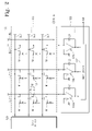
- FIG. 2 is a schematic circuit diagram of an x-ray detector according to an exemplary embodiment of the present invention shown in FIG. 1 ;
- FIGS. 3A to 3D and 4 A to 4 D are signal timing diagrams illustrating waveforms of the x-ray detector according to the exemplary embodiment of the present invention shown in FIG. 2 .
- first,” “second,” “third” etc. may be used herein to describe various elements, components, regions, layers and/or sections, these elements, components, regions, layers and/or sections should not be limited by these terms. These terms are only used to distinguish one element, component, region, layer or section from another element, component, region, layer or section. Thus, a first element, component, region, layer or section discussed below could be termed a second element, component, region, layer or section without departing from the teachings of the present invention.
- relative terms such as “lower” or “bottom” and “upper” or “top” may be used herein to describe one element's relationship to other elements as illustrated in the Figures. It will be understood that relative terms are intended to encompass different orientations of the device in addition to the orientation depicted in the Figures. For example, if the device in one of the figures is turned over, elements described as being on the “lower” side of other elements would then be oriented on the “upper” side of the other elements. The exemplary term “lower” can, therefore, encompass both an orientation of “lower” and “upper,” depending upon the particular orientation of the figure.
- Exemplary embodiments of the present invention are described herein with reference to cross section illustrations which are schematic illustrations of idealized embodiments of the present invention. As such, variations from the shapes of the illustrations as a result, for example, of manufacturing techniques and/or tolerances, are to be expected. Thus, embodiments of the present invention should not be construed as limited to the particular shapes of regions illustrated herein but are to include deviations in shapes which result, for example, from manufacturing. For example, a region illustrated or described as flat may, typically, have rough and/or nonlinear features. Moreover, sharp angles which are illustrated may be rounded. Thus, the regions illustrated in the figures are schematic in nature and their shapes are not intended to illustrate the precise shape of a region and are not intended to limit the scope of the present invention.
- FIG. 1 is a view showing an exemplary embodiment of an X-ray system.
- an X-ray system 200 includes an X-ray generator 210 that generates X-rays 211 in a direction toward a predetermined region 51 of a patient 50 (that is, an inspection region), an X-ray detector 100 that detects X-rays 211 which have passed through the predetermined region 51 of the patient 50 , and a display apparatus 220 that displays an image by receiving image signals corresponding to the X-rays 211 detected by the X-ray detector 100 .
- an X-ray system 200 is described with respect to the imaging of a patient 50 , it would be clear to one of ordinary skill in the art that such an exemplary embodiment of an X-ray system 200 may be applied to a wide range of applications wherein X-ray imaging is desired, e.g., luggage inspection, etc.
- the scintillator 170 provided between a flat panel 110 of the X-ray detector 100 and the patient 50 converts the X-ray 211 , which has passed through the patient 50 , into green light to provide the green light to the flat panel 110 .
- the X-ray detector 100 may be described in detail with reference to FIG. 2 .
- the X-ray detector 100 obtains image signals corresponding to X-rays 211 , which have passed through the patient 50 , and then provides the image signal to the display apparatus 220 . Accordingly, the display apparatus 220 may display the X-ray images corresponding to the image signals in real time. As an example of the present invention, the display apparatus 220 may include a liquid crystal display (“LCD”), and various other display types as would be known to one of ordinary skill in the art.
- LCD liquid crystal display
- FIG. 2 is a schematic circuit diagram of an x-ray detector according to an exemplary embodiment the present invention shown in FIG. 1 .
- an x-ray detector 100 includes a flat panel 110 which includes a plurality of light detecting pixels PP.
- Each light detecting pixel PP of the plurality of light detecting pixels PP detects an x-ray emitted from an x-ray generator 210 ( FIG. 1 ) and photoelectrically converts the detected x-ray to output an electrical signal proportional to the detected x-ray.
- the flat panel 110 further includes gate lines GL which extend substantially in parallel with each other in a first direction, e.g., a row direction, and data lines DL which extend substantially in parallel with each other in a second direction perpendicular to the first direction, e.g., in a column direction.
- a plurality of areas is formed in a substantially matrix configuration by the gate lines GL and the data lines DL in the flat panel 110 , and the light detecting pixels PP are disposed in respective areas of the plurality of areas.
- a first gate line GL 1 a first gate line GL 1 , a second gate line GL 2 and a third gate line GL 3 , as well as a first data line DL 1 , a second data line DL 2 and a third data line DL 3 are shown, but alternative exemplary embodiments are not limited thereto.
- the areas include one of the light detecting pixels PP, and each of the light detecting pixels PP includes a photodiode PD and a transistor Tr.
- the photodiode PD detects an x-ray emitted from an x-ray generator 210 and converts the detected x-ray into an electrical signal to output the electrical signal.
- the photodiode PD includes a first electrode connected to an input electrode of the transistor Tr and a second electrode connected to a bias line BL to which a bias voltage Vbias is applied.
- the bias voltage Vbias has a voltage level in a range of approximately ⁇ 5V to approximately ⁇ 10V.
- the bias voltage Vbias reverse biases the photodiode PD and, more particularly maintains the photodiode PD in a reverse bias state, as will be described below with reference to FIGS. 3 and 4 .
- a control electrode of the transistor Tr is electrically connected to a gate driver 120 through a corresponding gate line GL, and an output electrode of the transistor Tr is electrically connected to a readout integrated circuit 130 through a corresponding data line DL.
- a node to which the first electrode of the photodiode PD and the input electrode of the transistor Tr are connected is referred to as a coupling node N 1 .
- each light detecting pixel PP includes an associated coupling node N 1 disposed between the photodiode PD and the transistor Tr associated therewith.
- the gate driver 120 generates a gate signal and sequentially applies the gate signal to the first, second and third gate lines GL 1 , GL 2 and GL 3 , respectively.
- the gate signal is a voltage signal and swings between a gate-on voltage which turns on the transistor Tr and a gate-off voltage which turns off the transistor Tr.
- the gate-on voltage has a voltage level of approximately 15V
- the gate-off voltage has a voltage level of approximately ⁇ 10V, but alternative exemplary embodiments are not limited thereto.
- the electrical signal output from the photodiode PD is applied to a corresponding data line DL through the turned-on transistor Tr. Therefore, the data line DL transmits the electrical signal output from the transistor Tr to the readout integrated circuit 130 . Further, since the light detecting pixels PP are turned on row by row in response to the gate signal sequentially supplied to the gate lines GL from the gate driver 120 , the electrical signal is transmitted to the readout integrated circuit 130 on a row by row basis, e.g., based on the gate signal.
- the readout integrated circuit 130 includes a plurality of amplifiers 131 a , 131 b and 131 c and, more specifically, a first amplifier 131 a , a second amplifier 131 b and a third amplifier 131 c connected to the first data line DL 1 , the second data line DL 2 and the third data line DL 3 , respectively, as shown in FIG. 2 .
- the readout integrated circuit 130 includes a multiplexer 132 connected to respective output terminals of the plurality of amplifiers 131 a , 131 b and 131 c .
- the first, second and third amplifiers 131 a , 131 b and 131 c is an operational amplifier (“OP AMP”), but alternative exemplary embodiments are not limited thereto.
- a negative input terminal (“ ⁇ ”) of each of the first, second and third amplifiers 131 a , 131 b and 131 c , respectively, is connected to a corresponding data line DL, e.g., to the first data line DL 1 , the second data line DL 2 and the third data line DL 3 , respectively, to receive the electrical signal output from a corresponding light detecting pixel PP, and a positive input terminal (“+”) of each of the first, second and third amplifiers 131 a , 131 b and 131 c , respectively, receives a reference voltage.
- the reference voltage is a ground voltage.
- first, second and third capacitors C 1 , C 2 , and C 3 are connected between the negative input terminal ( ⁇ ) and an output terminal of each of the first amplifier 131 a , the second amplifier 131 b and the third amplifier 131 c.
- Input terminals of the multiplexer 132 are connected to corresponding output terminals of each of the first, second and third amplifiers 131 a , 131 b and 131 c , respectively, to receive a signal output therefrom.
- a signal OUT output from the multiplexer 132 is applied to a control circuit (not shown) arranged on a main board, for example, of the x-ray detector 100 and is converted to a digital signal by an analog-to-digital converter (not shown) in the control circuit.
- the digital signal is transmitted as an image signal to a display device 220 ( FIG. 1 ) connected to the x-ray detector 100 .
- the display device displays an x-ray image corresponding to the image signal provided from the x-ray detector 100 on a screen of the display device.
- FIGS. 3 a to 3 d are signal timing diagrams illustrating waveforms of an x-ray detector according to an exemplary embodiment of the present invention. More specifically, FIG. 3 a is a signal timing diagram showing when an x-ray is provided to the photodiode PD of the x-ray detector 100 according to an exemplary embodiment, FIG. 3 b is a signal timing diagram showing when a gate signal is applied to the gate line GL of the x-ray detector 100 ,
- FIG. 3 c is a signal timing diagram showing when a light is provided from a light generating sheet 115 ( FIG. 1 ) of the x-ray detector
- FIG. 3 d is a signal timing diagram showing an electric potential at the coupling node N 1 of the x-ray detector 100 .
- a driving period of the x-ray detector 100 (best shown in FIG. 2 ) includes an x-ray detecting period PI, a signal deleting period PE, and an offset control period P 0 .
- the x-ray detecting period PI includes a period during which an x-ray, generated during an x-ray generating period XR, from the x-ray generator is received by the light detecting pixel pp ( FIG. 2 ) and an electrical signal corresponding to the x-ray generated during the x-ray generating period XR is generated.
- the photodiode PD ( FIG. 2 ) is biased in a forward direction, and an electric potential at the coupling node N 1 to which the photodiode PD and the transistor Tr are connected decreases from a first voltage VA 1 at which the coupling node N 1 is at the beginning of the x-ray detecting period PI.
- the first voltage VA 1 is an initial voltage of the coupling node N 1 .
- the electric potential at the coupling node N 1 decreases to a second voltage VA 2 until a first time point t 1 , at which the generation of the x-ray is stopped, e.g., until the end of the x-ray generating period XR of the x-ray detecting period PI.
- the gate signal applied to the control electrode of the transistor Tr transitions from the gate-off voltage Voff to the gate-on voltage Von at a second time point t 2 .
- the transistor Tr is turned on (in response to the gate-on voltage Von) during a first gate-on period GE between the second time point t 2 and a third time point t 3 , e.g., during a time period in which the gate signal is maintained at the gate-on voltage Von.
- the electric potential at the coupling node N 1 gradually increases back to the first voltage VA 1 , as shown in FIG. 3 d.
- the transistor Tr is turned off at the third time point t 3 , when the gate signal transitions to the gate-off voltage Voff, and the electric potential at the coupling node N 1 is thereby lowered to a third voltage VA 3 .
- the third voltage VA 3 is less than the first voltage VA 1 but greater than the second voltage VA 2 . Since the transistor Tr is turned off at the third time point t 3 , the electric potential at the coupling node N 1 is maintained at the third voltage VA 3 , as shown in FIG. 3 d . Therefore, the x-ray detecting period PI is substantially defined as being from the initial time point t 0 to the third time point t 3 .
- the signal deleting period PE which is a period in which the electric potential charged to the coupling node N 1 during the x-ray detecting period PI is removed such that the electric potential at the coupling node N 1 returns to an initial state, thereby effectively preventing a previous signal, e.g., a previous signal from the light detecting pixel PP, from affecting, e.g., interfering with and/or mixing with, a next signal.
- the signal deleting period PE begins at a fourth time point t 4 , at which time the light generating sheet (not shown) generates a light which saturates the photodiode PD, as shown in FIG. 3 c.
- the light generating sheet includes an inorganic light emitting material and therewith provides the light to the flat panel 110 ( FIG. 2 ) of the x-ray detector 100 during a second flash period FE.
- the photodiode PD is again biased in the forward direction, and the electric potential at the coupling node N 1 decreases to a fourth voltage VA 4 until a fifth time point t 5 at which the supply of the light is stopped, as shown in FIG. 3 c .
- the electric potential at the coupling node N 1 is maintained at the fourth voltage VA 4 until a sixth time point t 6 .
- the gate signal transitions to the gate-on voltage Von, and the transistor Tr is turned on during a third gate-on period GT between the sixth time point t 6 and a seventh time point t 7 , as shown in FIG. 3 b .
- the electric potential at the coupling node N 1 thereby increases back to the first voltage VA 1 during the third gate-on period GT. Therefore, a previous signal is completely removed from the coupling node N 1 , and the electric potential at the coupling node N 1 is thereby initialized.
- the signal deleting period PE is defined from the fourth time point t 4 to the seventh time point t 7 .
- the offset control period P 0 begins after the signal deleting period PE.
- the offset control period P 0 includes at least one first flash period F 0 during, which the light is generated by the light generating sheet, and at least one second gate-on period G 0 , during which the gate signal is at the gate-on voltage to turn on the transistor Tr. More specifically, the first flash period F 0 is maintained during a time interval in which the photodiode PD ( FIG. 2 ) is saturated and the second gate-on period G 0 , during which the gate signal transitions to the gate-on voltage Von after the first flash period F 0 .
- the first flash period F 0 and/or the second gate-on period G 0 may occur more than once, e.g., repeatedly, during a single offset control period P 0 .
- the first flash periods F 0 may have a same time width dt, e.g., a duration dt, but alternative exemplary embodiments are not limited thereto.
- durations of the first flash periods F 0 and/or the second gate-on periods G 0 may be varied, as will be described in further detail below with reference to FIG. 4 .
- the electric potential at the coupling node N 1 decreases between an eighth time point t 8 , at which the first flash period F 0 begins, and is eventually lowered to the fourth voltage VA 4 at a ninth time point t 9 , at which the first flash period F 0 is finished. Then, the second gate-on period G 0 begins at a tenth time point t 10 at which the gate signal transitions to the gate-on voltage Von, as shown in FIG. 3 b .
- the electric potential at the coupling node N 1 increases during the second gate-on period G 0 and reaches the first voltage VA 1 at an eleventh time point t 11 , e.g., at a time point at which the second gate-on period G 0 ends.
- the electric potential at the coupling node N 1 is uniformly maintained at the first voltage VA 1 even when the second gate-on period G 0 is removed, since the first flash period F 0 and the second gate-on period G 0 occur.
- the offset control period P 0 is therefore defined as being from the eighth time point t 8 , at which the light, e.g., an optical flash, is generated, to a subsequent initial time point t 0 , e.g., when a next x-ray is generated in the next x-ray generating period XR.
- the electric potential at the coupling node N 1 of the x-ray detector 100 is uniformly maintained at the first voltage VA 1 at the initial time point t 0 when the next x-ray is generated in the offset control period P 0 . Therefore, an offset voltage deviation is substantially reduced and/or effectively prevented in the x-ray detector 100 according to an exemplary embodiment.
- FIGS. 4 a to 4 d are signal timing diagrams illustrating waveforms of an x-ray detector according to an alternative exemplary embodiment of the present invention.
- FIG. 4 a is a signal timing diagram showing when an x-ray is provided to the photodiode PD of the x-ray detector 100 according to an exemplary embodiment of the present invention
- FIG. 4 b is a signal timing diagram showing when a gate signal applied to the gate line GL of the x-ray detector 100
- FIG. 4 c is a signal timing diagram showing when a light is provided from a light generating sheet (not shown) according to an alternative exemplary embodiment of the present invention
- FIG. 4 a is a signal timing diagram showing when an x-ray is provided to the photodiode PD of the x-ray detector 100 according to an exemplary embodiment of the present invention
- FIG. 4 b is a signal timing diagram showing when a gate signal applied to the gate line GL of the x-ray detector 100
- FIG. 4 c
- FIG. 4 d is a signal timing diagram showing an electric potential at the coupling node N 1 of the x-ray detector 100 according to an alternative exemplary embodiment.
- the same reference characters in FIG. 4 refer to the same or like components as shown in FIG. 3 , and any repetitive detailed description thereof has been omitted.
- the driving period of the x-ray detector 100 (best shown in FIG. 2 ) includes an x-ray detecting period PI, a signal deleting period PE and an offset control period P 0 .
- the offset control period P 0 begins after the signal deleting period PE, as shown in FIG. 4 d .
- the offset control period P 0 includes a first flash period F 0 during which a light is generated from a light generating sheet 115 ( FIG. 1 ) and a second gate-on period G 0 during which a gate signal which turns on the transistor Tr is output.
- the second gate-on period G 0 according to an exemplary embodiment is a period during which the gate signal transitions to the gate-on voltage Von and, more particularly, begins after the first flash period F 0 , as shown in FIG. 4 c.
- first flash period F 0 and the second gate-on period P 0 occur repeatedly during a given offset control period P 0 .
- first flash periods F 0 which occur during the given offset control period P 0 have different time widths, e.g., durations, from each other. More specifically, consecutive first flash periods F 0 according to an exemplary embodiment have a first time width dt 1 , a second time width dt 2 and/or a third time width dt 3 .
- each first flash period F 0 is maintained over a time period during which the photodiode PD is saturated by the light from the light generating sheet.
- the electric potential at the coupling node N 1 decreases from an eighth time point t 8 , at which the first flash period F 0 begins, and is decreases to a fourth voltage VA 4 at a ninth time point t 9 , at which the first flash period F 0 ends, as shown in FIG. 4 c .
- the second gate-on period G 0 begins at a tenth time point t 10 , at which point the gate signal transitions to the gate-on voltage Von.
- the electric potential at the coupling node N 1 increases during the second gate-on period G 0 and reaches the first voltage VA 1 at an eleventh time point t 11 , at which the second gate-on period G 0 ends.
- the electric potential at the coupling node N 1 is uniformly maintained at the first voltage VA 1 at a time when the second gate-on period G 0 .
- the offset control period P 0 is defined as being the eighth time point t 8 , at which an optical flash, e.g., the light, is generated to a subsequent initial point t 0 at which point a next x-ray is generated during the next x-ray generating period XR, as shown in FIG. 4 a . Therefore, the electric potential at the coupling node N 1 of the x-ray detector according to an exemplary embodiment of the present invention is uniformly maintained at the first voltage VA 1 at the initial point t 0 when the next x-ray is generated during the next offset control period P 0 .
- the x-ray is provided from the x-ray generator 210 ( FIG. 1 ) at irregular intervals, the electric potential at the coupling node N 1 is uniformly maintained. As a result, an image distortion, caused by an offset voltage deviation in the coupling node N 1 , is effectively prevented.
- an offset control period is provided between two x-ray detecting periods which turn on a switching device of a light detecting pixel to output an electrical signal corresponding to an x-ray.
- the x-ray detecting period includes a first gate-on period transmitting the gate signal to turn on the switching device of the light detecting pixel, and the offset control period includes flash periods which apply light to the photodiode and a second gate-on period which transmits the gate signal which turns on the switching device of the light detecting pixel in a period where the light is not applied.
- an electric potential at a coupling node of a photodiode and a switching device is uniformly maintained at an end time point of a gate-on period, thereby effectively preventing image distortion caused by an offset voltage deviation.
Landscapes
- Engineering & Computer Science (AREA)
- Multimedia (AREA)
- Signal Processing (AREA)
- Physics & Mathematics (AREA)
- Health & Medical Sciences (AREA)
- Life Sciences & Earth Sciences (AREA)
- General Physics & Mathematics (AREA)
- High Energy & Nuclear Physics (AREA)
- Molecular Biology (AREA)
- Spectroscopy & Molecular Physics (AREA)
- Transforming Light Signals Into Electric Signals (AREA)
- Measurement Of Radiation (AREA)
Abstract
Description
Claims (16)
Applications Claiming Priority (2)
| Application Number | Priority Date | Filing Date | Title |
|---|---|---|---|
| KR10-2008-0027472 | 2008-03-25 | ||
| KR1020080027472A KR20090102185A (en) | 2008-03-25 | 2008-03-25 | Method of driding x-ray detector and x-ray detector using the same |
Publications (2)
| Publication Number | Publication Date |
|---|---|
| US20090245465A1 US20090245465A1 (en) | 2009-10-01 |
| US8071951B2 true US8071951B2 (en) | 2011-12-06 |
Family
ID=40810178
Family Applications (1)
| Application Number | Title | Priority Date | Filing Date |
|---|---|---|---|
| US12/409,546 Expired - Fee Related US8071951B2 (en) | 2008-03-25 | 2009-03-24 | Method of driving x-ray detector and x-ray detector using the same |
Country Status (5)
| Country | Link |
|---|---|
| US (1) | US8071951B2 (en) |
| EP (1) | EP2106123A3 (en) |
| JP (1) | JP5506179B2 (en) |
| KR (1) | KR20090102185A (en) |
| CN (1) | CN101545978A (en) |
Families Citing this family (14)
| Publication number | Priority date | Publication date | Assignee | Title |
|---|---|---|---|---|
| KR101107168B1 (en) * | 2010-01-04 | 2012-01-25 | 삼성모바일디스플레이주식회사 | X-ray detection device and driving method thereof |
| KR101107164B1 (en) | 2010-01-14 | 2012-01-25 | 삼성모바일디스플레이주식회사 | X-ray detection device and driving method thereof |
| KR101156445B1 (en) | 2010-05-14 | 2012-06-18 | 삼성모바일디스플레이주식회사 | Driving method for light sensing pixel and X-ray detector including thereof |
| KR101042958B1 (en) * | 2010-06-09 | 2011-06-20 | 삼성모바일디스플레이주식회사 | X-ray detector and x-ray image detection method |
| KR101158100B1 (en) * | 2010-06-28 | 2012-06-22 | (주)세현 | X-ray detecting apparatus and x-ray detecting system having the same |
| KR101126582B1 (en) | 2011-07-29 | 2012-03-23 | 주식회사 뷰웍스 | Apparatus for detecting x-ray and operating method thereof |
| KR101413202B1 (en) | 2012-06-27 | 2014-06-27 | 주식회사 레이언스 | X-ray detector and method for driving the same |
| US9078569B2 (en) * | 2012-08-20 | 2015-07-14 | Zhengrong Ying | Configurable data measurement and acquisition systems for multi-slice X-ray computed tomography systems |
| KR20150061704A (en) * | 2013-11-27 | 2015-06-05 | 삼성전자주식회사 | X-ray detector, imaging apparatus having the same and control method for the same |
| CN106575075B (en) * | 2014-07-21 | 2018-10-12 | 万睿视影像有限公司 | With the low-power imager that function is automatically sensed |
| JP6780291B2 (en) * | 2016-05-16 | 2020-11-04 | コニカミノルタ株式会社 | X-ray imaging device |
| WO2020228935A1 (en) | 2019-05-13 | 2020-11-19 | Direct Conversion Ab | Method of reading out data in a radiation detector, radiation detector and imaging apparatus |
| KR102344857B1 (en) | 2020-03-31 | 2021-12-29 | 신정훈 | Intraoral X-ray sensor and manufacturing method thereof |
| KR20230072148A (en) | 2021-11-17 | 2023-05-24 | 신정훈 | Intraoral X-ray sensor and manufacturing method thereof |
Citations (4)
| Publication number | Priority date | Publication date | Assignee | Title |
|---|---|---|---|---|
| EP1176814A2 (en) | 2000-07-28 | 2002-01-30 | Canon Kabushiki Kaisha | Photoelectric conversion device, radiation detection apparatus, image processing system, and driving method thereof |
| EP1378942A1 (en) | 2002-07-05 | 2004-01-07 | Kabushiki Kaisha Toshiba | Radation detector that adjusts offset component |
| US6980246B1 (en) | 1999-07-06 | 2005-12-27 | Trixell S.A.S. | Process for controlling a photosensitive device including a photosensitive point produced by techniques for depositing semiconductor materials |
| EP1179741B1 (en) | 2000-08-11 | 2007-09-19 | Canon Kabushiki Kaisha | Image sensing apparatus |
Family Cites Families (6)
| Publication number | Priority date | Publication date | Assignee | Title |
|---|---|---|---|---|
| JP3630832B2 (en) * | 1996-03-28 | 2005-03-23 | キヤノン株式会社 | Photoelectric conversion device |
| JP3740435B2 (en) * | 2001-06-07 | 2006-02-01 | キヤノン株式会社 | Radiation imaging apparatus, driving method thereof, and radiation imaging system |
| JP4211435B2 (en) * | 2002-08-30 | 2009-01-21 | 株式会社島津製作所 | Radiation detector |
| JP4416471B2 (en) * | 2003-10-17 | 2010-02-17 | キヤノン株式会社 | Digital X-ray imaging apparatus and drive control program thereof |
| JP4834518B2 (en) * | 2005-11-29 | 2011-12-14 | キヤノン株式会社 | Radiation imaging apparatus, control method therefor, and recording medium on which program for executing the same is recorded |
| JP4921180B2 (en) * | 2006-01-25 | 2012-04-25 | キヤノン株式会社 | Radiation detection apparatus and radiation imaging system |
-
2008
- 2008-03-25 KR KR1020080027472A patent/KR20090102185A/en not_active Withdrawn
- 2008-10-09 JP JP2008263031A patent/JP5506179B2/en active Active
-
2009
- 2009-01-09 CN CN200910000146A patent/CN101545978A/en active Pending
- 2009-01-17 EP EP09000631A patent/EP2106123A3/en not_active Withdrawn
- 2009-03-24 US US12/409,546 patent/US8071951B2/en not_active Expired - Fee Related
Patent Citations (5)
| Publication number | Priority date | Publication date | Assignee | Title |
|---|---|---|---|---|
| US6980246B1 (en) | 1999-07-06 | 2005-12-27 | Trixell S.A.S. | Process for controlling a photosensitive device including a photosensitive point produced by techniques for depositing semiconductor materials |
| EP1176814A2 (en) | 2000-07-28 | 2002-01-30 | Canon Kabushiki Kaisha | Photoelectric conversion device, radiation detection apparatus, image processing system, and driving method thereof |
| EP1176814A3 (en) | 2000-07-28 | 2008-05-28 | Canon Kabushiki Kaisha | Photoelectric conversion device, radiation detection apparatus, image processing system, and driving method thereof |
| EP1179741B1 (en) | 2000-08-11 | 2007-09-19 | Canon Kabushiki Kaisha | Image sensing apparatus |
| EP1378942A1 (en) | 2002-07-05 | 2004-01-07 | Kabushiki Kaisha Toshiba | Radation detector that adjusts offset component |
Non-Patent Citations (1)
| Title |
|---|
| Extended European Search Report for application No. 09000631.3-2202 dated Aug. 3, 2011. |
Also Published As
| Publication number | Publication date |
|---|---|
| JP2009236897A (en) | 2009-10-15 |
| KR20090102185A (en) | 2009-09-30 |
| EP2106123A2 (en) | 2009-09-30 |
| CN101545978A (en) | 2009-09-30 |
| US20090245465A1 (en) | 2009-10-01 |
| EP2106123A3 (en) | 2011-08-31 |
| JP5506179B2 (en) | 2014-05-28 |
Similar Documents
| Publication | Publication Date | Title |
|---|---|---|
| US8071951B2 (en) | Method of driving x-ray detector and x-ray detector using the same | |
| US7724874B2 (en) | Radiation imaging apparatus, driving method thereof and radiation imaging system | |
| DE102019117491B4 (en) | TOUCH-SENSITIVE DISPLAY DEVICE, MICROCONTROLLER AND CONTROL METHODS | |
| US9128196B2 (en) | Radiation imaging apparatus and radiation imaging system | |
| US20150179696A1 (en) | Photodetector circuit and semiconductor device | |
| US20160299587A1 (en) | Touch display screen and time division driving method thereof | |
| CA2766545A1 (en) | Sensing apparatus and sensing method | |
| CN101442603A (en) | Imaging apparatus, and radiation imaging system | |
| JP5178710B2 (en) | Display device | |
| CN110971843B (en) | Radiographic apparatus, control method thereof, and radiographic system | |
| US20140320685A1 (en) | Imaging apparatus and imaging system | |
| CN103828342B (en) | Imaging device, imaging system, and the method controlling imaging device | |
| US8624196B2 (en) | X-ray detector and driving method thereof | |
| KR20140087695A (en) | Display device including sensing unit and driving method thereof | |
| KR20110080052A (en) | X-ray detection device and driving method thereof | |
| US20180293948A1 (en) | Driving device for liquid crystal panel and driving method for the same | |
| CN102906674B (en) | With the display device of touch sensor | |
| US20130113768A1 (en) | Display device and drive method for same | |
| US20130120332A1 (en) | Display device | |
| US8723096B2 (en) | Active photosensing pixel with two-terminal photosensing transistor | |
| US8445829B2 (en) | Active photosensing pixel | |
| US20120113060A1 (en) | Sensor circuit and display apparatus | |
| KR101278899B1 (en) | Active photosensing pixel | |
| JP2007094407A5 (en) | ||
| CN102376277B (en) | Active light-sensing pixel, active light-sensing array and light-sensing method |
Legal Events
| Date | Code | Title | Description |
|---|---|---|---|
| AS | Assignment |
Owner name: SAMSUNG ELECTRONICS CO., LTD., KOREA, REPUBLIC OF Free format text: ASSIGNMENT OF ASSIGNORS INTEREST;ASSIGNORS:JUNG, KWAN-WOOK;GOO, KYUNG-SANG;CHOO, DAE-HO;REEL/FRAME:022437/0698 Effective date: 20081202 |
|
| ZAAA | Notice of allowance and fees due |
Free format text: ORIGINAL CODE: NOA |
|
| ZAAB | Notice of allowance mailed |
Free format text: ORIGINAL CODE: MN/=. |
|
| STCF | Information on status: patent grant |
Free format text: PATENTED CASE |
|
| FEPP | Fee payment procedure |
Free format text: PAYOR NUMBER ASSIGNED (ORIGINAL EVENT CODE: ASPN); ENTITY STATUS OF PATENT OWNER: LARGE ENTITY |
|
| AS | Assignment |
Owner name: SAMSUNG DISPLAY CO., LTD., KOREA, REPUBLIC OF Free format text: ASSIGNMENT OF ASSIGNORS INTEREST;ASSIGNOR:SAMSUNG ELECTRONICS CO., LTD.;REEL/FRAME:029093/0177 Effective date: 20120904 |
|
| FPAY | Fee payment |
Year of fee payment: 4 |
|
| MAFP | Maintenance fee payment |
Free format text: PAYMENT OF MAINTENANCE FEE, 8TH YEAR, LARGE ENTITY (ORIGINAL EVENT CODE: M1552); ENTITY STATUS OF PATENT OWNER: LARGE ENTITY Year of fee payment: 8 |
|
| FEPP | Fee payment procedure |
Free format text: MAINTENANCE FEE REMINDER MAILED (ORIGINAL EVENT CODE: REM.); ENTITY STATUS OF PATENT OWNER: LARGE ENTITY |
|
| LAPS | Lapse for failure to pay maintenance fees |
Free format text: PATENT EXPIRED FOR FAILURE TO PAY MAINTENANCE FEES (ORIGINAL EVENT CODE: EXP.); ENTITY STATUS OF PATENT OWNER: LARGE ENTITY |
|
| STCH | Information on status: patent discontinuation |
Free format text: PATENT EXPIRED DUE TO NONPAYMENT OF MAINTENANCE FEES UNDER 37 CFR 1.362 |
|
| FP | Lapsed due to failure to pay maintenance fee |
Effective date: 20231206 |