US8071458B1 - Method for forming an interfacial passivation layer on the Ge semiconductor - Google Patents
Method for forming an interfacial passivation layer on the Ge semiconductor Download PDFInfo
- Publication number
- US8071458B1 US8071458B1 US12/953,601 US95360110A US8071458B1 US 8071458 B1 US8071458 B1 US 8071458B1 US 95360110 A US95360110 A US 95360110A US 8071458 B1 US8071458 B1 US 8071458B1
- Authority
- US
- United States
- Prior art keywords
- layer
- germanium
- interfacial
- semiconductor
- germanium semiconductor
- Prior art date
- Legal status (The legal status is an assumption and is not a legal conclusion. Google has not performed a legal analysis and makes no representation as to the accuracy of the status listed.)
- Expired - Fee Related
Links
- 238000000034 method Methods 0.000 title claims abstract description 63
- 239000004065 semiconductor Substances 0.000 title claims abstract description 57
- 238000002161 passivation Methods 0.000 title claims abstract description 23
- 239000012212 insulator Substances 0.000 claims abstract description 48
- 230000008569 process Effects 0.000 claims abstract description 40
- 239000012530 fluid Substances 0.000 claims abstract description 37
- 238000000137 annealing Methods 0.000 claims abstract description 18
- VYPSYNLAJGMNEJ-UHFFFAOYSA-N Silicium dioxide Chemical compound O=[Si]=O VYPSYNLAJGMNEJ-UHFFFAOYSA-N 0.000 claims description 39
- 229910052732 germanium Inorganic materials 0.000 claims description 37
- GNPVGFCGXDBREM-UHFFFAOYSA-N germanium atom Chemical compound [Ge] GNPVGFCGXDBREM-UHFFFAOYSA-N 0.000 claims description 37
- YBMRDBCBODYGJE-UHFFFAOYSA-N germanium oxide Inorganic materials O=[Ge]=O YBMRDBCBODYGJE-UHFFFAOYSA-N 0.000 claims description 28
- 238000005516 engineering process Methods 0.000 claims description 17
- 229910052782 aluminium Inorganic materials 0.000 claims description 12
- XAGFODPZIPBFFR-UHFFFAOYSA-N aluminium Chemical compound [Al] XAGFODPZIPBFFR-UHFFFAOYSA-N 0.000 claims description 12
- CURLTUGMZLYLDI-UHFFFAOYSA-N Carbon dioxide Chemical compound O=C=O CURLTUGMZLYLDI-UHFFFAOYSA-N 0.000 claims description 10
- 229940119177 germanium dioxide Drugs 0.000 claims description 8
- BDERNNFJNOPAEC-UHFFFAOYSA-N propan-1-ol Chemical compound CCCO BDERNNFJNOPAEC-UHFFFAOYSA-N 0.000 claims description 8
- 238000002207 thermal evaporation Methods 0.000 claims description 8
- 238000004518 low pressure chemical vapour deposition Methods 0.000 claims description 7
- PVADDRMAFCOOPC-UHFFFAOYSA-N oxogermanium Chemical compound [Ge]=O PVADDRMAFCOOPC-UHFFFAOYSA-N 0.000 claims description 7
- 229910002092 carbon dioxide Inorganic materials 0.000 claims description 5
- 239000001569 carbon dioxide Substances 0.000 claims description 5
- 238000000407 epitaxy Methods 0.000 claims description 4
- XLYOFNOQVPJJNP-UHFFFAOYSA-N water Substances O XLYOFNOQVPJJNP-UHFFFAOYSA-N 0.000 claims description 4
- 229910044991 metal oxide Inorganic materials 0.000 claims description 3
- 150000004706 metal oxides Chemical group 0.000 claims description 3
- 229910052814 silicon oxide Inorganic materials 0.000 claims description 3
- 238000012545 processing Methods 0.000 claims description 2
- 239000000377 silicon dioxide Substances 0.000 description 18
- 230000007547 defect Effects 0.000 description 13
- 235000012239 silicon dioxide Nutrition 0.000 description 10
- 238000010586 diagram Methods 0.000 description 9
- 239000010408 film Substances 0.000 description 9
- 238000009792 diffusion process Methods 0.000 description 7
- 238000004519 manufacturing process Methods 0.000 description 7
- 239000003990 capacitor Substances 0.000 description 6
- 239000007800 oxidant agent Substances 0.000 description 5
- 230000001590 oxidative effect Effects 0.000 description 5
- 230000005540 biological transmission Effects 0.000 description 4
- 239000000969 carrier Substances 0.000 description 4
- 238000006243 chemical reaction Methods 0.000 description 4
- 230000003247 decreasing effect Effects 0.000 description 4
- 238000000151 deposition Methods 0.000 description 4
- 230000008021 deposition Effects 0.000 description 4
- 238000011161 development Methods 0.000 description 4
- 239000000758 substrate Substances 0.000 description 4
- XUIMIQQOPSSXEZ-UHFFFAOYSA-N Silicon Chemical compound [Si] XUIMIQQOPSSXEZ-UHFFFAOYSA-N 0.000 description 3
- 230000015572 biosynthetic process Effects 0.000 description 3
- 230000005669 field effect Effects 0.000 description 3
- CJNBYAVZURUTKZ-UHFFFAOYSA-N hafnium(iv) oxide Chemical compound O=[Hf]=O CJNBYAVZURUTKZ-UHFFFAOYSA-N 0.000 description 3
- 229910052710 silicon Inorganic materials 0.000 description 3
- 239000010703 silicon Substances 0.000 description 3
- 238000004833 X-ray photoelectron spectroscopy Methods 0.000 description 2
- 238000004458 analytical method Methods 0.000 description 2
- 238000000231 atomic layer deposition Methods 0.000 description 2
- 230000008901 benefit Effects 0.000 description 2
- 238000005229 chemical vapour deposition Methods 0.000 description 2
- 230000005284 excitation Effects 0.000 description 2
- 229910000449 hafnium oxide Inorganic materials 0.000 description 2
- WIHZLLGSGQNAGK-UHFFFAOYSA-N hafnium(4+);oxygen(2-) Chemical compound [O-2].[O-2].[Hf+4] WIHZLLGSGQNAGK-UHFFFAOYSA-N 0.000 description 2
- 239000012535 impurity Substances 0.000 description 2
- 239000000463 material Substances 0.000 description 2
- 238000001000 micrograph Methods 0.000 description 2
- 238000001451 molecular beam epitaxy Methods 0.000 description 2
- 239000002086 nanomaterial Substances 0.000 description 2
- 150000004767 nitrides Chemical class 0.000 description 2
- UCKMPCXJQFINFW-UHFFFAOYSA-N Sulphide Chemical compound [S-2] UCKMPCXJQFINFW-UHFFFAOYSA-N 0.000 description 1
- 238000009825 accumulation Methods 0.000 description 1
- 230000004913 activation Effects 0.000 description 1
- VXAUWWUXCIMFIM-UHFFFAOYSA-M aluminum;oxygen(2-);hydroxide Chemical compound [OH-].[O-2].[Al+3] VXAUWWUXCIMFIM-UHFFFAOYSA-M 0.000 description 1
- 230000015556 catabolic process Effects 0.000 description 1
- 239000003638 chemical reducing agent Substances 0.000 description 1
- 239000003795 chemical substances by application Substances 0.000 description 1
- 150000001875 compounds Chemical class 0.000 description 1
- 238000007796 conventional method Methods 0.000 description 1
- 230000008878 coupling Effects 0.000 description 1
- 238000010168 coupling process Methods 0.000 description 1
- 238000005859 coupling reaction Methods 0.000 description 1
- 238000006731 degradation reaction Methods 0.000 description 1
- 239000002019 doping agent Substances 0.000 description 1
- 230000000694 effects Effects 0.000 description 1
- BIXHRBFZLLFBFL-UHFFFAOYSA-N germanium nitride Chemical compound N#[Ge]N([Ge]#N)[Ge]#N BIXHRBFZLLFBFL-UHFFFAOYSA-N 0.000 description 1
- 238000005468 ion implantation Methods 0.000 description 1
- 239000007788 liquid Substances 0.000 description 1
- 229910052751 metal Inorganic materials 0.000 description 1
- 239000002184 metal Substances 0.000 description 1
- 238000012986 modification Methods 0.000 description 1
- 230000004048 modification Effects 0.000 description 1
- -1 nitride germanium oxide Chemical class 0.000 description 1
- 230000000704 physical effect Effects 0.000 description 1
- 229910021420 polycrystalline silicon Inorganic materials 0.000 description 1
- 238000002203 pretreatment Methods 0.000 description 1
- 238000011160 research Methods 0.000 description 1
- 230000004044 response Effects 0.000 description 1
- 238000004544 sputter deposition Methods 0.000 description 1
- 239000000126 substance Substances 0.000 description 1
- 238000005979 thermal decomposition reaction Methods 0.000 description 1
- 239000010409 thin film Substances 0.000 description 1
Images


Classifications
-
- H—ELECTRICITY
- H01—ELECTRIC ELEMENTS
- H01L—SEMICONDUCTOR DEVICES NOT COVERED BY CLASS H10
- H01L21/00—Processes or apparatus adapted for the manufacture or treatment of semiconductor or solid state devices or of parts thereof
- H01L21/02—Manufacture or treatment of semiconductor devices or of parts thereof
- H01L21/02104—Forming layers
- H01L21/02107—Forming insulating materials on a substrate
- H01L21/02109—Forming insulating materials on a substrate characterised by the type of layer, e.g. type of material, porous/non-porous, pre-cursors, mixtures or laminates
- H01L21/02112—Forming insulating materials on a substrate characterised by the type of layer, e.g. type of material, porous/non-porous, pre-cursors, mixtures or laminates characterised by the material of the layer
- H01L21/02123—Forming insulating materials on a substrate characterised by the type of layer, e.g. type of material, porous/non-porous, pre-cursors, mixtures or laminates characterised by the material of the layer the material containing silicon
- H01L21/02164—Forming insulating materials on a substrate characterised by the type of layer, e.g. type of material, porous/non-porous, pre-cursors, mixtures or laminates characterised by the material of the layer the material containing silicon the material being a silicon oxide, e.g. SiO2
-
- H—ELECTRICITY
- H01—ELECTRIC ELEMENTS
- H01L—SEMICONDUCTOR DEVICES NOT COVERED BY CLASS H10
- H01L21/00—Processes or apparatus adapted for the manufacture or treatment of semiconductor or solid state devices or of parts thereof
- H01L21/02—Manufacture or treatment of semiconductor devices or of parts thereof
- H01L21/02104—Forming layers
- H01L21/02107—Forming insulating materials on a substrate
- H01L21/02296—Forming insulating materials on a substrate characterised by the treatment performed before or after the formation of the layer
- H01L21/02318—Forming insulating materials on a substrate characterised by the treatment performed before or after the formation of the layer post-treatment
- H01L21/02343—Forming insulating materials on a substrate characterised by the treatment performed before or after the formation of the layer post-treatment treatment by exposure to a liquid
-
- H—ELECTRICITY
- H01—ELECTRIC ELEMENTS
- H01L—SEMICONDUCTOR DEVICES NOT COVERED BY CLASS H10
- H01L21/00—Processes or apparatus adapted for the manufacture or treatment of semiconductor or solid state devices or of parts thereof
- H01L21/02—Manufacture or treatment of semiconductor devices or of parts thereof
- H01L21/04—Manufacture or treatment of semiconductor devices or of parts thereof the devices having at least one potential-jump barrier or surface barrier, e.g. PN junction, depletion layer or carrier concentration layer
- H01L21/18—Manufacture or treatment of semiconductor devices or of parts thereof the devices having at least one potential-jump barrier or surface barrier, e.g. PN junction, depletion layer or carrier concentration layer the devices having semiconductor bodies comprising elements of Group IV of the Periodic System or AIIIBV compounds with or without impurities, e.g. doping materials
- H01L21/28—Manufacture of electrodes on semiconductor bodies using processes or apparatus not provided for in groups H01L21/20 - H01L21/268
- H01L21/28008—Making conductor-insulator-semiconductor electrodes
- H01L21/28255—Making conductor-insulator-semiconductor electrodes the insulator being formed after the semiconductor body, the semiconductor belonging to Group IV and not being elemental silicon, e.g. Ge, SiGe, SiGeC
Definitions
- the invention relates to a method for forming a protection layer on the semiconductor, particularly to a method for forming an interfacial passivation layer on the germanium semiconductor.
- the development trend for the manufacturing technology of the integrated circuit (IC) is still kept to the trend of miniaturizing transistor size, in order to reach the goal of high efficacy and high density.
- Due to the efficacy of conventional polycrystalline silicon/silicon dioxide/silicon channel metal-oxide-semiconductor field effect transistor is unable to be increased by the miniaturizing technology, thus, how to increase the mobility of carrier and the dielectric capacitance of gate has become the key technology and goal for the development of field effect transistor in the next generation.
- the mobility for the electron and hole of Ge semiconductor is 2 times and 4 times higher than those of silicon, respectively.
- the basic process is similar to the silicon semiconductor technology.
- the germanium metal-oxide-semiconductor field-effect transistor (Ge-MOSFET) has been considered as the most promising candidate for the next generation of semiconductor industry.
- germanium dioxide GeO 2
- silicon dioxide SiO 2
- high-k high dielectric constant
- hafnium dioxide HfO 2
- Al 2 O 3 aluminum dioxide
- the sulfide such as H 2 S or SF 6 is used to form an interface on semiconductor surface.
- the process is still a conventional method, and the interface has to be formed before gate insulator layer deposition.
- the interface is unable to be formed after the gate insulator deposition, and the defect generation in gate insulator could occur again during sequent thermal process.
- the plasma method is used to form the germanium nitride, the germanium dioxide or the nitride germanium oxide as the interface. Although it is a low-temperature process, it requires the vacuum system, only the interface is able to be formed. The interface is unable to be formed after the gate insulator deposition, and the defects could generate in gate insulator during sequent thermal process.
- the invention relates to a method for forming an interfacial passivation layer in the Ge semiconductor. It is able to form a high-quality interfacial layer made by low-temperature process between the Ge semiconductor and gate dielectric layer. Thus, it is able to be used in the advanced semiconductor technology.
- the invention can be applied for the pre-treatment of Ge surface before the formation of gate dielectric layer. It also can be applied after the formation of gate dielectric layer or after the high-temperature thermal annealing process.
- the quality of gate insulator layer can be improved, and flat and high-quality Ge/gate interfacial passivation layer can be formed in order to simplify the semiconductor process.
- the supercritical fluid technology of the invention can be applied to mend the degraded dielectric characteristics after the thermal annealing process, so that the gate-first process can be applied to the Ge transistor process.
- the Ge-MOSFET may have high gate capacitance, and have more smooth interfacial protection layer and better carrier mobility, in order to form a high efficient Ge-MOSFET component with high on-current.
- the invention can rebuild the interface destroyed by a series of high-temperature thermal process (such as higher than 400° C.) via low-temperature of supercritical fluid process, and passivate the electric defect caused by the Ge diffused into the insulator layer.
- the invention can add the oxidant or reducing agent into supercritical carbon dioxide fluid, it can penetrate through the gate insulator layer and form the protection chemical compound layer on the surface of Ge semiconductor at low temperature (such as below 200° C.).
- the invention employs low-temperature (about 150° C.) supercritical fluid technology to passivate the defect of gate insulator layer, and avoid the use of conventional high-temperature process (greater than 400° C.), in order to reduce the thermal budget and inhibit the Ge diffusion effect.
- the hafnium dioxide (HfO 2 ) deposited by the electronic gun can be used as the gate dielectric layer of Ge-MOSFET.
- the chemical bond is strengthened after the treatment, which proves that the gate insulator layer can be penetrated by the low-temperature supercritical fluid treatment technology.
- the invention can be applied in Ge-MOSFET field with high-k dielectric gate insulator layer.
- Due to the invention can form an interfacial passivation layer with good quality under low-temperature process of 150° C., thus the development of technology has great innovation and advancement.
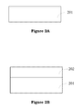
- FIG. 1A to FIG. 1D show the first embodiment for a method for forming an interfacial passivation layer on the Ge semiconductor of the invention.
- FIG. 2A to FIG. 2E show the second embodiment for a method for forming an interfacial passivation layer on the Ge semiconductor after thermal annealing of the invention.
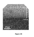
- FIG. 3A shows the transmission electron microscope image of SiO 2 /Ge interface before the supercritical fluid treatment.
- FIG. 3B shows the transmission electron microscope image of SiO 2 /Ge interface after the supercritical fluid treatment.
- FIG. 4A and FIG. 4B show the capacitance-voltage relation diagram after the supercritical fluid treatment under different frequency and temperature.
- FIG. 5 shows the “capacitance-voltage characteristic diagram”.
- the insert is the corresponding characteristic of gate leakage current density with and without SCF treatment after post dielectric annealing.
- FIG. 6 shows the bond analysis diagram of x-ray photoelectron spectroscopy for hafnium oxide MOSFET with and without SCF treatment.
- the invention relates to a method for forming an interfacial passivation layer on the germanium (Ge) semiconductor.
- the detail of FIG. 1A to FIG. 1D in the first embodiment is described as follows:
- the general epitaxy technology (such as Molecular Beam Epitaxy process, Metal-Organic Chemical Vapor Deposition process) is employed to deposit a Ge semiconductor layer 101 (about 2.5 ⁇ m thick).
- the Low Pressure Chemical Vapor Deposition System is employed to deposit a silicon dioxide (SiO 2 ) layer 102 (about 12 nm thick) on the Ge semiconductor layer 101 (including P-type Ge semiconductor layer or N-type Ge semiconductor layer), which is used as the gate insulator layer.
- LPCVD Low Pressure Chemical Vapor Deposition System
- the thermal evaporation process is employed to form an aluminum film 103 A on the silicon dioxide layer (insulator layer) 102 , which is used as the electrode 103 A above the aluminum film of MOS Capacitor.
- the thermal evaporation process is employed to form an aluminum film 103 B below the Ge semiconductor layer 101 , which is used as the electrode 103 B below the aluminum film of MOS Capacitor.
- the invention relates to a method for forming an interfacial passivation layer on the Ge semiconductor after thermal annealing.
- the detail of FIG. 2A to FIG. 2E in the second embodiment is described as follows:
- the general epitaxy technology (such as Molecular Beam Epitaxy process, Metal-Organic Chemical Vapor Deposition process) is employed to deposit a Ge semiconductor layer 201 (about 2.5 u, thick).
- the Low Pressure Chemical Vapor Deposition System is employed to deposit a silicon dioxide (SiO 2 ) layer 202 (about 12 nm thick) on the Ge semiconductor layer 201 (including P-type Ge semiconductor layer or N-type Ge semiconductor layer), which is used as the gate insulator layer.
- LPCVD Low Pressure Chemical Vapor Deposition System
- the annealing treatment is performed for the silicon dioxide layer (insulator layer) 202 and the Ge semiconductor layer 201 at about 400° C.
- the thermal evaporation process is employed to form an aluminum film 203 A on the silicon dioxide layer (insulator layer) 202 , which is used as the upper electrode 203 A above the aluminum film of MOS Capacitor.
- the thermal evaporation process is employed to form an aluminum film 203 B below the Ge semiconductor layer 201 , which is used as the bottom electrode 203 B below the aluminum film of MOS Capacitor.
- the electronic gun also can be used to deposit a hafnium dioxide (HfO 2 ) insulator layer (13 nm thick), which can be used to substitute the silicon dioxide layer (insulator layer) 202 as the gate dielectric layer.
- HfO 2 hafnium dioxide
- the insulator layer used in the invention includes the metal oxide, silicon oxide, and germanium oxide.
- the physical properties of supercritical fluid are similar to liquid and gas.
- the supercritical fluid has high diffusion coefficient and low surface tension, which can penetrate into nano-structure effectively, and prevent the damage of nano-structure.
- the supercritical fluid has high dissolving ability and high transmitting ability, which can carry the oxidant (H 2 O in the invention) deeply to the interface between the insulator and germanium substrate for the reaction effectively, in order to form a good interfacial passivation layer.
- the transmission electron microscope (TEM) image of SiO 2 /Ge interface before the supercritical fluid treatment is illustrated.
- FIG. 3B the transmission electron microscope (TEM) image of SiO 2 /Ge interface after the supercritical fluid treatment is illustrated. Compare these two figures, it is found that the Ge surface after the supercritical fluid treatment has much clearer and more smooth interfacial layer.
- the capacitance-voltage relation diagram after the supercritical fluid treatment is illustrated under different frequency and temperature.
- the capacitance in inversion area positive bias area
- the inversion capacitance is generated from a minor carriers via the surface defect of Ge semiconductor through the thermal excitation.
- the frequency is increased, the generation of carriers is unable to catch up with the frequency response, so that the inversion capacitance is decreased gradually.
- FIG. 4B when the temperature is reduced to 80K, there is no significant difference for the inversion capacitance no matter the supercritical fluid treatment is performed or not.
- the inversion capacitance is generated from a minor carriers via the surface defect of Ge semiconductor through the thermal excitation.
- the carriers are unable to be generated due to the energy loss.
- the frequency is as low as 10 KHz, the inversion capacitance is also unable to be appeared.
- the inversion capacitance of component is reduced after the supercritical fluid treatment at room temperature, and the speed of component is faster than the component without treatment. It is known that after the supercritical fluid treatment, the surface defect of component is reduced, and the generation of high-frequency inversion capacitance is inhibited.
- the accumulation capacitance after thermal annealing treatment (negative bias area) is lowest. It shows the annealing treatment will degrade the interface between the Ge and insulator layer. After thermal annealing treatment and supercritical fluid treatment, the accumulated capacitance will recover to nearly initial capacitance value. It shows that the supercritical fluid treatment can mend the degradation of interfacial layer on Ge semiconductor, and rebuild good interfacial layer between the Ge and insulator layer.
- the “gate leakage current diagram” at upper right area it is found that high-temperature thermal annealing process will increase the leakage current of Ge-MOSFET.
- the gate leakage current will be reduced significantly, even reduced to nearly the original value.
- the “capacitance-voltage characteristic diagram” and the “gate leakage current diagram” it is shown that high-temperature thermal annealing process will destroy the interface between the Ge and insulator layer, and may cause the thermal diffusion of Ge into the insulator layer to form new leakage current route.
- the supercritical fluid treatment it is able to rebuild good Ge interfacial layer effectively, and passivate the defect formed by Ge diffusion. Thus, it is able to reduce the gate leakage current.
- FIG. 6 shows the bond analysis diagram of x-ray photoelectron spectroscopy for hafnium oxide MOSFET. It is found from FIG. 6 that after the supercritical fluid treatment, Ge 3d (represent the bond among germanium element) is decreased by 18.86%, but GeO 2 (germanium oxide interfacial layer with less interfacial layer state defect intensity) is increase by 17.56%. It shows after the supercritical fluid treatment, the germanium element on the interface can be oxidized effectively, and high-quality germanium dioxide interfacial passivation layer can be formed. It also shows the supercritical fluid treatment is able to penetrate the deposited dielectric layer, and use the oxidant or nitride agent carried by the fluid molecule to react on the interface.
- the invention relates to a manufacturing process of Ge-MOSFET.
- the Ge semiconductor and LPCVD SiO 2 are employed in the MOS capacitor as gate dielectric insulator layer.
- the low-temperature supercritical fluid (SF) treatment technology can increase the quality of component interface, and mend the gate leakage current after high-temperature thermal annealing process.
- the good interfacial layer formed in the invention is able to reduce the interfacial defect between the gate insulator layer and Ge semiconductor.
- the low-temperature supercritical fluid is able to form high-quality interfacial layer between the Ge semiconductor and gate insulator layer, and is able to improve the quality of gate insulator layer degraded by the thermal annealing process.
Abstract
Description
Claims (9)
Applications Claiming Priority (2)
| Application Number | Priority Date | Filing Date | Title |
|---|---|---|---|
| TW99127661A | 2010-08-19 | ||
| TW099127661A TWI413185B (en) | 2010-08-19 | 2010-08-19 | A method for forming an interfacial passivation layer in the ge semiconductor |
Publications (1)
| Publication Number | Publication Date |
|---|---|
| US8071458B1 true US8071458B1 (en) | 2011-12-06 |
Family
ID=45034385
Family Applications (1)
| Application Number | Title | Priority Date | Filing Date |
|---|---|---|---|
| US12/953,601 Expired - Fee Related US8071458B1 (en) | 2010-08-19 | 2010-11-24 | Method for forming an interfacial passivation layer on the Ge semiconductor |
Country Status (2)
| Country | Link |
|---|---|
| US (1) | US8071458B1 (en) |
| TW (1) | TWI413185B (en) |
Cited By (5)
| Publication number | Priority date | Publication date | Assignee | Title |
|---|---|---|---|---|
| US8691636B2 (en) * | 2012-01-03 | 2014-04-08 | National Chiao Tung University | Method for removing germanium suboxide |
| US8987096B2 (en) * | 2012-02-07 | 2015-03-24 | United Microelectronics Corp. | Semiconductor process |
| CN112151384A (en) * | 2020-08-17 | 2020-12-29 | 西安交通大学 | Supercritical nitrogen oxide based improvement on 4H-SiC/SiO2Low-temperature processing method of interface and application thereof |
| US20210134974A1 (en) * | 2019-10-31 | 2021-05-06 | Taiwan Semiconductor Manufacturing Company, Ltd. | Transistors with Reduced Defect and Methods Forming Same |
| CN113555422A (en) * | 2021-07-14 | 2021-10-26 | 西安电子科技大学 | Based on supercritical CO2Treated Ga2O3Metal oxide semiconductor field effect transistor and preparation method thereof |
Family Cites Families (5)
| Publication number | Priority date | Publication date | Assignee | Title |
|---|---|---|---|---|
| US7122880B2 (en) * | 2002-05-30 | 2006-10-17 | Air Products And Chemicals, Inc. | Compositions for preparing low dielectric materials |
| US20050130449A1 (en) * | 2003-12-15 | 2005-06-16 | Ping Chuang | Method of forming an oxide layer using a mixture of a supercritical state fluid and an oxidizing agent |
| TWI416738B (en) * | 2006-03-21 | 2013-11-21 | Semiconductor Energy Lab | Nonvolatile semiconductor memory device |
| TWI431726B (en) * | 2006-06-01 | 2014-03-21 | Semiconductor Energy Lab | Nonvolatile semiconductor memory device |
| US7977121B2 (en) * | 2006-11-17 | 2011-07-12 | Air Products And Chemicals, Inc. | Method and composition for restoring dielectric properties of porous dielectric materials |
-
2010
- 2010-08-19 TW TW099127661A patent/TWI413185B/en not_active IP Right Cessation
- 2010-11-24 US US12/953,601 patent/US8071458B1/en not_active Expired - Fee Related
Non-Patent Citations (2)
| Title |
|---|
| Liu et al, Po-Tsun; Effects of Postgate Dielectric Treatment on Germanium-Based Metal-Oxide-Semiconductor Device by Supercritical Fluid Technology; Applied Physics Letters 96, 112902-1-112902-3, American Institute of Physics 2010. |
| Liu, P. et al. (Mar. 17, 2010). Effects of postgate dielectric treatment on germanium-based metal-oxide-semiconductor device by supercritical fluid technology. Applied Physics Letters, 96, 112902. * |
Cited By (8)
| Publication number | Priority date | Publication date | Assignee | Title |
|---|---|---|---|---|
| US8691636B2 (en) * | 2012-01-03 | 2014-04-08 | National Chiao Tung University | Method for removing germanium suboxide |
| US8987096B2 (en) * | 2012-02-07 | 2015-03-24 | United Microelectronics Corp. | Semiconductor process |
| US20210134974A1 (en) * | 2019-10-31 | 2021-05-06 | Taiwan Semiconductor Manufacturing Company, Ltd. | Transistors with Reduced Defect and Methods Forming Same |
| US11264478B2 (en) * | 2019-10-31 | 2022-03-01 | Taiwan Semiconductor Manufacturing Company, Ltd. | Transistors with reduced defect and methods forming same |
| CN112151384A (en) * | 2020-08-17 | 2020-12-29 | 西安交通大学 | Supercritical nitrogen oxide based improvement on 4H-SiC/SiO2Low-temperature processing method of interface and application thereof |
| CN112151384B (en) * | 2020-08-17 | 2022-02-11 | 西安交通大学 | Supercritical nitrogen oxide based improvement on 4H-SiC/SiO2Low-temperature processing method of interface and application thereof |
| CN113555422A (en) * | 2021-07-14 | 2021-10-26 | 西安电子科技大学 | Based on supercritical CO2Treated Ga2O3Metal oxide semiconductor field effect transistor and preparation method thereof |
| CN113555422B (en) * | 2021-07-14 | 2023-03-10 | 西安电子科技大学 | Based on supercritical CO 2 Treated Ga 2 O 3 Metal oxide semiconductor field effect transistor and preparation method thereof |
Also Published As
| Publication number | Publication date |
|---|---|
| TW201209917A (en) | 2012-03-01 |
| TWI413185B (en) | 2013-10-21 |
Similar Documents
| Publication | Publication Date | Title |
|---|---|---|
| US9779946B2 (en) | System and method for mitigating oxide growth in a gate dielectric | |
| US7723781B2 (en) | Vertical thin-film transistor with enhanced gate oxide | |
| US7820552B2 (en) | Advanced high-k gate stack patterning and structure containing a patterned high-k gate stack | |
| US9059314B2 (en) | Structure and method to obtain EOT scaled dielectric stacks | |
| TWI447913B (en) | Replacement metal gate transistors with reduced gate oxide leakage | |
| US7037816B2 (en) | System and method for integration of HfO2 and RTCVD poly-silicon | |
| US8071458B1 (en) | Method for forming an interfacial passivation layer on the Ge semiconductor | |
| US20080050870A1 (en) | Method for fabricating semiconductor device | |
| Alam et al. | Effect of surface preparation and interfacial layer on the quality of SiO2/GaN interfaces | |
| US6921703B2 (en) | System and method for mitigating oxide growth in a gate dielectric | |
| Ishii et al. | High electron mobility metal–insulator–semiconductor field-effect transistors fabricated on (111)-oriented InGaAs channels | |
| Watanabe et al. | Gate stack technology for advanced high-mobility Ge-channel metal-oxide-semiconductor devices–Fundamental aspects of germanium oxides and application of plasma nitridation technique for fabrication of scalable oxynitride dielectrics | |
| US7138339B2 (en) | Method of manufacturing semiconductor device including etching a conductive layer by using a gas including SiCl4 and NF3 | |
| US8691636B2 (en) | Method for removing germanium suboxide | |
| Liu et al. | Wet thermal annealing effect on TaN/HfO2/Ge metal—oxide—semiconductor capacitors with and without a GeO2 passivation layer | |
| Lee et al. | Liquid-phase-deposited SiO2 on AlGaAs and its application | |
| Huang et al. | Interface Trap Density Reduction Due to AlGeO Interfacial Layer Formation by Al Capping on Al 2 O 3/GeO x/Ge Stack | |
| Arith | 4H-SiC metal oxide semiconductor devices | |
| JP2005079563A (en) | Manufacturing method for electronic device | |
| Hellström et al. | Interfacial layer engineering using thulium silicate/germanate for high-k/metal gate MOSFETs | |
| Lim et al. | Improvements in electrical characteristics of plasma enhanced chemical vapor deposition-Tetraethylorthosilicate–SiO2 by atomic hydrogen passivation via hot-wire technique | |
| Lee et al. | Electrical Characteristics of Metal-Oxide-Semiconductor Capacitor with High-κ/Metal Gate Using Oxygen Scavenging Process | |
| JP2004265973A (en) | Method for manufacturing semiconductor device | |
| Ju et al. | A novel in situ plasma treatment for damage-free metal/high-k gate stack RIE process | |
| Lee et al. | Post-cleaning effect on a HfO2 gate stack using a NF3/NH3 plasma |
Legal Events
| Date | Code | Title | Description |
|---|---|---|---|
| AS | Assignment |
Owner name: NATIONAL CHIAO TUNG UNIVERSITY, TAIWAN Free format text: ASSIGNMENT OF ASSIGNORS INTEREST;ASSIGNORS:LIU, PO-TSUN;HUANG, CHEN-SHUO;HUANG, YI-LIN;AND OTHERS;SIGNING DATES FROM 20101028 TO 20101122;REEL/FRAME:025418/0768 |
|
| AS | Assignment |
Owner name: NATIONAL CHIAO TUNG UNIVERSITY, TAIWAN Free format text: ASSIGNMENT OF ASSIGNORS INTEREST;ASSIGNOR:NISHI, YOSHIO;REEL/FRAME:026672/0798 Effective date: 20110715 |
|
| ZAAA | Notice of allowance and fees due |
Free format text: ORIGINAL CODE: NOA |
|
| ZAAB | Notice of allowance mailed |
Free format text: ORIGINAL CODE: MN/=. |
|
| STCF | Information on status: patent grant |
Free format text: PATENTED CASE |
|
| FPAY | Fee payment |
Year of fee payment: 4 |
|
| MAFP | Maintenance fee payment |
Free format text: PAYMENT OF MAINTENANCE FEE, 8TH YR, SMALL ENTITY (ORIGINAL EVENT CODE: M2552); ENTITY STATUS OF PATENT OWNER: SMALL ENTITY Year of fee payment: 8 |
|
| FEPP | Fee payment procedure |
Free format text: MAINTENANCE FEE REMINDER MAILED (ORIGINAL EVENT CODE: REM.); ENTITY STATUS OF PATENT OWNER: SMALL ENTITY |
|
| LAPS | Lapse for failure to pay maintenance fees |
Free format text: PATENT EXPIRED FOR FAILURE TO PAY MAINTENANCE FEES (ORIGINAL EVENT CODE: EXP.); ENTITY STATUS OF PATENT OWNER: SMALL ENTITY |
|
| STCH | Information on status: patent discontinuation |
Free format text: PATENT EXPIRED DUE TO NONPAYMENT OF MAINTENANCE FEES UNDER 37 CFR 1.362 |
|
| FP | Lapsed due to failure to pay maintenance fee |
Effective date: 20231206 |