US8064863B1 - Image rejection calibration - Google Patents
Image rejection calibration Download PDFInfo
- Publication number
- US8064863B1 US8064863B1 US12/371,018 US37101809A US8064863B1 US 8064863 B1 US8064863 B1 US 8064863B1 US 37101809 A US37101809 A US 37101809A US 8064863 B1 US8064863 B1 US 8064863B1
- Authority
- US
- United States
- Prior art keywords
- receiver front
- phase
- test signal
- error
- input
- Prior art date
- Legal status (The legal status is an assumption and is not a legal conclusion. Google has not performed a legal analysis and makes no representation as to the accuracy of the status listed.)
- Active, expires
Links
Images


Classifications
-
- H—ELECTRICITY
- H04—ELECTRIC COMMUNICATION TECHNIQUE
- H04B—TRANSMISSION
- H04B1/00—Details of transmission systems, not covered by a single one of groups H04B3/00 - H04B13/00; Details of transmission systems not characterised by the medium used for transmission
- H04B1/06—Receivers
- H04B1/16—Circuits
- H04B1/30—Circuits for homodyne or synchrodyne receivers
Definitions
- the present invention relates to a radio frequency receiver, and more particularly relates to image rejection calibration in a radio frequency receiver.
- a received signal is downconverted to an intermediate frequency (IF), rather than to baseband, for signal processing using a mixing operation.
- IF intermediate frequency
- One inherent problem in heterodyne receivers is that when downconverting the received signal to the desired intermediate frequency, an image of the received signal is also converted to the desired intermediate frequency as a result of the mixing operation. More specifically, because the mixing operation does not preserve the polarity of the difference between its two input frequencies, the receive frequency and the image frequency, which are located at an equal distance from either side of a local oscillator (LO) frequency used in the mixing operation, are translated to the same IF frequency. Since power of the image signal may not be regulated and can be much higher than that of the desired signal, image rejection must be performed.
- LO local oscillator
- the present invention relates to image rejection calibration in a radio frequency receiver.
- the receiver includes a receiver front-end and an image rejection calibration system.
- the image rejection calibration system provides a first test signal to a radio frequency (RF) input of the receiver front-end, and obtains first measurements of a quadrature output signal output from the receiver front-end while the first test signal is applied to the RF input.
- the image rejection calibration system then applies a second test signal to the RF input of the receiver that is approximately 90 degrees out-of-phase with the first test signal, and obtains second measurements of the quadrature output signal output from the receiver front-end while the second test signal is applied to the RF input.
- the image rejection calibration system determines an amplitude error and a phase error of the receiver front-end.
- the image rejection calibration system then applies an amplitude correction and a phase correction to the receiver front-end to correct for the amplitude error and the phase error of the receiver front-end.
- the amplitude and phase errors of the receiver front-end are separated from amplitude and phase errors of the image rejection calibration system.
- the amplitude correction corrects for the amplitude error of the receiver front-end rather than a combined amplitude error of the receiver front-end and the image rejection calibration system
- the phase correction corrects for the phase error of the receiver front-end rather than a combined phase error of the receiver front-end and the image rejection calibration system
- the receiver includes a receiver front-end having a first stage and a second stage interconnected via a polyphase filter.
- the receiver includes an image rejection calibration system.
- the image rejection calibration system applies a first test signal to an RF input of the receiver front-end, where an image of the first test signal is at a frequency within a high attenuation frequency zone of the polyphase filter.
- the image rejection calibration system obtains first measurements of a quadrature output signal output from the receiver front-end while the first test signal is applied to the RF input of the receiver front-end.
- the image rejection calibration system then applies a second test signal that is approximately 90 degrees out-of-phase with the first test signal to the RF input of the receiver front-end.
- the image of the second test signal is at a frequency within a high-attenuation frequency zone of the polyphase filter.
- the image rejection calibration system obtains second measurements of the quadrature signal output from the receiver front-end while the second test signal is applied to the RF input. Since the images of the first and second test signals are located within the high-attenuation frequency zone of the polyphase filter, the first and second measurements are indicative of an amplitude error and a phase error of the second stage of the receiver front-end.
- the polyphase filter is set to a bypass mode.
- the image rejection calibration system obtains measurements of the quadrature output signal output from the receiver front-end while two test signals that are approximately 90 degrees out-of-phase are applied to the RF input of the receiver front-end, and determines an amplitude error and phase error of the first stage based on these measurements and the measurements indicative of the amplitude error and the phase error of the second stage.
- the image rejection calibration system then applies an amplitude correction and a phase correction to the first stage.
- the image rejection calibration system may also apply corrections for the amplitude and phase errors of the second stage or provide the amplitude and phase errors of the second stage to a digital processor for correction.
- FIG. 1 illustrates a radio frequency transceiver including a receiver having an image rejection calibration system according to one embodiment of the present invention
- FIG. 2 is a block diagram of the receiver of FIG. 1 wherein the receiver includes an image rejection calibration system according to one embodiment of the present invention
- FIG. 3 is a flow chart illustrating the operation of the image rejection calibration system of FIG. 2 according to one embodiment of the present invention
- FIG. 4 is a block diagram of digital image rejection calibration control circuitry of the image rejection calibration system of FIG. 2 according to one embodiment of the present invention
- FIG. 5 is a block diagram of measurement circuitry of the digital image rejection calibration control circuitry according to one embodiment of the present invention.
- FIGS. 6-9 are flow charts illustrating the operation of the image rejection calibration system of FIG. 2 according to a second embodiment of the present invention.
- the present invention relates to image rejection calibration for a radio frequency (RF) receiver.
- RF radio frequency
- the transceiver 10 can be partitioned into a digital processor 12 and a radio section 14 .
- a transmitter 16 receives transmit signals (I T and Q T ) from the digital processor 12 and outputs a corresponding RF transmit signal (X T ) to an antenna 18 via a duplexer or switch 20 .
- the radio section 14 also includes a receiver 22 that receives a received RF signal (X R ) from the antenna 18 and outputs corresponding receive signals (I R and Q R ) to the digital processor 12 .
- the transmitter 16 includes a modulator, which generates the RF transmit signal (X T ) from orthogonal baseband transmit signals (I T ) and (Q T ), and the receiver 22 includes a demodulator, which generates the orthogonal downconverted receive signals (I R ) and (Q R ) from the received RF signal (X R ).
- the present invention relates to calibration of the receiver 22 for the mismatch errors resulting in an amplitude, or gain, error (a R ) causing the in-phase receive signal (I R ) to be amplified by a factor of 1+a R relative to the quadrature-phase receive signal (Q R ) and a phase error ( ⁇ R ) causing the phase difference between the nominally orthogonal signals to be 90°+ ⁇ R .
- a R amplitude, or gain, error
- ⁇ R phase error
- FIG. 2 illustrates the receiver 22 according to one embodiment of the present invention.
- the receiver 22 includes a receiver front-end 24 and an image rejection calibration (IRC) system 26 that performs image rejection calibration according to one embodiment of the present invention.
- IRC image rejection calibration
- the receiver front-end 24 includes a low noise amplifier (LNA) 28 , a first stage 30 , a polyphase notch filter 32 , and a second stage 34 connected as shown.
- the first stage 30 includes I/Q mixing circuitry 36 that operates to downconvert an amplified received signal output by the LNA 28 to a desired very low intermediate frequency (VLIF) using two substantially orthogonal local oscillator (LO) signals from a LO generation circuit to provide a quadrature output signal at the VLIF.
- the LO generation circuit is formed by a LO 38 and a divider 40 . Note that the while in this embodiment the receiver 22 is a VLIF receiver, the present invention is not limited thereto.
- the receiver 22 may alternatively downconvert the received signal to baseband.
- the quadrature output signal output by the I/Q mixing circuitry 36 passes through a phase correction circuit 42 , which operates to provide a phase correction under control of the IRC system 26 as described below.
- a post mixing amplifier (PMA) 44 then amplifies the output of the phase correction circuit 42 .
- An amplitude correction (A CORRECTION ) is applied to vary a gain of the PMA 44 to correct for an amplitude error determined by the IRC system 26 .
- the output of the PMA 44 is then filtered by a second order Bessel filter 46 to provide a quadrature output signal of the first stage 30 of the receiver front-end 24 .
- the quadrature output signal from the first stage 30 is then filtered by a polyphase filter, which in this embodiment is the polyphase notch filter 32 .
- a polyphase filter is a filter having different responses for a main signal and an image of that main signal such that the image is attenuated with respect to the main signal.
- the output of the polyphase notch filter 32 is provided as a quadrature input signal to the second stage 34 of the receiver front-end 24 .
- the second stage 34 of the receiver front-end 24 includes R/2R networks 48 and 50 , variable gain amplifiers (VGAs) 52 and 54 , and analog-to-digital converters (ADCs) 56 and 58 connected as shown.
- VGAs variable gain amplifiers
- ADCs analog-to-digital converters
- the illustrated embodiments of the first and second stages 30 and 34 of the receiver front-end 24 are exemplary. As will be appreciated by one of ordinary skill in the art, the receiver front-end 24 may vary depending on the particular implementation. Further, while in this embodiment the receiver front-end 24 includes the first and second stages 30 and 34 that are separated by the polyphase notch filter 32 , the present invention is not limited thereto. In another embodiment, the receiver front-end 24 may not include a polyphase filter dividing the receiver front-end 24 into two stages.
- the IRC system 26 includes an IRC modulator 60 that provides a modulated signal to an RF phase shifter 62 .
- the RF phase shifter 62 has two states that are approximately 90 degrees apart.
- the output of the RF phase shifter 62 is provided to an RF input of the receiver front-end 24 via an injection amplifier 64 as a test signal.
- the RF input of the receiver front-end 24 is the input of the LNA 28 .
- the IRC modulator 60 includes digital intermediate frequency (IF) circuitry 66 and an I/Q modulator 68 .
- the digital IF circuitry 66 operates to generate in-phase and a quadrature-phase analog signals at the VLIF of the receiver 22 .
- the in-phase and quadrature-phase analog signals are square wave signals.
- the I/Q modulator 68 upconverts the in-phase and quadrature-phase analog signals from the digital IF circuitry 66 to the RF frequency of the receiver 22 using, in this embodiment, the same LO signals used by the receiver front-end 24 , and then combines the upconverted in-phase and quadrature-phase signals to provide the modulated signal to be output to the RF phase shifter 62 .
- the modulated signal output by the IRC modulator 60 is a single side-band signal. In the embodiment discussed below, the modulated signal is an upper side-band signal. However, in another embodiment, the modulated signal may be a lower side-band signal. Further, the IRC modulator 60 may be controllable to provide either the upper side-band or lower side-band signal as desired by controlling the phasing of the in-phase and quadrature-phase analog signals output by the digital IF circuitry 66 .
- the IRC system 26 includes digital IRC control circuitry 70 , which controls the IRC modulator 60 and the RF phase shifter 62 to provide test signals to the RF input of the receiver front-end 24 , measures amplitude and phase errors of a quadrature output signal output by the receiver front-end 24 via the ADCs 56 and 58 , determines amplitude and phase errors of the receiver front-end 24 , and applies correction factors to correct for the amplitude and phase errors of the receiver front-end 24 , as discussed below.
- the digital IRC control circuitry 70 is enabled to separate the amplitude and phase errors of the receiver front-end 24 from amplitude and phase errors of the IRC modulator 60 .
- the correction factors applied by the digital IRC control circuitry 70 correct for the amplitude and phase errors of the receiver front-end 24 rather than combined amplitude and phase errors of the receiver front-end 24 and the IRC modulator 60 .
- the IRC modulator 60 may be a non-ideal, relatively low power digital modulator without adversely affecting the accuracy of the image rejection calibration process.
- FIG. 3 is a flow chart illustrating the operation of the IRC system 26 of FIG. 2 according to one embodiment of the present invention. While this process is discussed with respect to the particular embodiment of the receiver 22 illustrated in FIG. 2 , the present invention is not limited thereto.
- the IRC system 26 may be utilized in any type of quadrature receiver.
- the digital IRC control circuitry 70 sets the polyphase notch filter 32 to a bypass mode (step 100 ). Of course, for embodiments where the receiver 22 does not include a polyphase filter dividing the receiver front-end 24 into two stages, step 100 is not needed.
- the digital IRC control circuitry 70 sets a phase shift of the RF phase shifter 62 to zero degrees (step 102 ).
- phase shifter 62 may use any two phase shifts that are approximately 90 degrees apart. Further, due to a phase error of the RF phase shifter 62 , the 90 degree phase shift has an error, which in an exemplary embodiment is ⁇ 4 degrees.
- the digital IRC control circuitry 70 obtains a first amplitude (or gain) error estimate (GE 0 ) and a first phase error estimate (PE 0 ) based on measurements of a quadrature output signal (I R , Q R ) output by the receiver front-end 24 while a first test signal is applied to the RF input of the receiver front-end 24 by the IRC modulator 60 and the RF phase shifter 62 (step 104 ).
- the digital IRC control circuitry 70 sets the phase shift of the RF phase shifter 62 to 90 degrees (step 106 ).
- the digital IRC control circuitry 70 obtains a second amplitude error estimate (GE 90 ) and a second phase error estimate (PE 90 ) based on measurements of the quadrature output signal (I R , Q R ) output by the receiver front-end 24 while a second test signal that is approximately 90 degrees out-of-phase with the first test signal is applied to the RF input of the receiver front-end 24 (step 108 ).
- GE 90 a second amplitude error estimate
- PE 90 phase error estimate
- the digital IRC control circuitry 70 determines an amplitude error (a R ) and a phase error ( ⁇ R ) of the receiver front-end 24 based on the first and second amplitude error estimates (GE 0 and GE 90 ) and the first and second phase error estimates (PE 0 and PE 90 ) (step 110 ) and applies corresponding amplitude and phase corrections (A CORRECTION and ⁇ CORRECTION ) to the receiver front-end 24 (step 112 ).
- the digital IRC control circuitry 70 is enabled to separate the amplitude error (a R ) of the receiver front-end 24 from any amplitude error of the IRC modulator 60 and separate the phase error ( ⁇ R ) of the receiver front-end 24 from any phase error of the IRC modulator 60 .
- the IRC system 26 corrects for the amplitude error (a R ) of the receiver front-end 24 rather than a combined amplitude error of the receiver front-end 24 and the IRC modulator 60 .
- the IRC system 26 corrects for the phase error ( ⁇ R ) of the receiver front-end 24 rather than a combined phase error of the receiver front-end 24 and the IRC modulator 60 .
- a T amplitude (or gain) error of the IRC modulator 60 ;
- ⁇ T1 phase error of the IRC modulator 60 ;
- ⁇ T2 phase error of the LO system used by the IRC modulator 60 ;
- a R amplitude (or gain) error of the receiver front-end 24 ;
- ⁇ R phase error of the receiver front-end 24 ;
- ⁇ phase error to 90 degrees of the RF phase shifter 62 .
- I 0 ⁇ je ⁇ j ⁇ ⁇ + ⁇ for a phase shift of 0 degrees
- Q 90 ⁇ je j ⁇ ⁇ + ⁇ for a phase shift of 90 degrees
- I 90 je j ⁇ ⁇ + ⁇ for a phase shift of 90 degrees
- Q 0 je ⁇ j ⁇ ⁇ + ⁇ for a phase shift of 0 degrees.
- the measurements of the quadrature output signal output from the receiver front-end 24 when the RF phase shifter 62 is set to 0 degrees may then be defined as:
- the digital IRC control circuitry 70 may then determine the amplitude error (a R ) of the receiver front-end 24 based on the equation:
- the digital IRC control circuitry 70 determines the amplitude error (a R ) of the receiver front-end 24 by first determining amplitude, or gain, error estimates using the measurements of the quadrature output signal output by the receiver front-end 24 based on the following equations:
- 0 ); and (20) PE 90 ang( I R ⁇ e ⁇ j ⁇ t
- the function ang( ) returns a phase of a complex term.
- the phase error ( ⁇ R ) of the receiver front-end 24 may be estimated as:
- FIG. 4 is a more detailed block diagram of the digital IRC control circuitry 70 of FIG. 2 according to one embodiment of the present invention.
- the digital IRC control circuitry 70 includes measurement circuitry 72 , registers 74 , and control circuitry 76 .
- the measurement circuitry 72 operates under the control of the control circuitry 76 to obtain measurements of the in-phase and quadrature-phase components of the quadrature output signal from the receiver front-end 24 ( FIG. 2 ) while the test signals are being applied to the RF input of the receiver front-end 24 .
- the measurement circuitry 72 obtains the measurements of the in-phase and quadrature-phase components of the quadrature output signal from the receiver front-end 24 while the test signals are being applied to the RF input of the receiver front-end 24 and outputs corresponding amplitude and phase error estimates (GE 0 , GE 90 , PE 0 , PE 90 ). Based on the output of the measurement circuitry 72 , the control circuitry 76 determines the amplitude error (a R ) and the phase error ( ⁇ R ) of the receiver front-end 24 .
- FIG. 5 is a more detailed block diagram of the measurement circuitry 72 of FIG. 4 according to one embodiment of the present invention.
- the measurement circuitry 72 includes multipliers 78 through 84 , accumulators 86 through 92 , and two coordinate rotation digital computers (CORDICs) 94 and 96 designated as a master CORDIC 94 and a slave CORDIC 96 .
- CORDICs coordinate rotation digital computers
- the multipliers 78 and 80 multiply the digital in-phase component (I R ) of the quadrature output signal from the receiver front-end 24 ( FIG.
- the master CORDIC 94 then processes the outputs of the accumulators 86 and 88 to provide a magnitude measurement of the term I R ⁇ e ⁇ j ⁇ t
- the multipliers 82 and 84 multiply the digital quadrature-phase component (Q R ) of the quadrature output signal from the receiver front-end 24 ( FIG. 2 ) with sine and cosine functions, respectively, and the accumulators 90 and 92 accumulate the outputs of the multipliers 82 and 84 , respectively.
- the outputs of the accumulators 90 and 92 in response to the test signal having the first phase shift of approximately 0 degrees provide a measured estimate of the term Q R ⁇ e ⁇ j ⁇ t
- the slave CORDIC 96 then processes the outputs of the accumulators 90 and 92 to provide a magnitude measurement of the term Q R ⁇ e ⁇ j ⁇ t
- the multipliers 78 and 80 multiply the digital in-phase component (I R ) of the quadrature output signal from the receiver front-end 24 ( FIG. 2 ) with sine and cosine functions, respectively, and the accumulators 86 and 88 accumulate the outputs of the multipliers 78 and 80 , respectively.
- the outputs of the accumulators 86 and 88 in response to the second test signal having the second phase shift of approximately 90 degrees provide a measured estimate of the term I R ⁇ e ⁇ j ⁇ t
- the master CORDIC 94 then processes the outputs of the accumulators 86 and 88 to provide a magnitude measurement of the term I R ⁇ e ⁇ j ⁇ t
- the multipliers 82 and 84 multiply the digital quadrature-phase component (Q R ) of the quadrature output signal from the receiver front-end 24 ( FIG. 2 ) with sine and cosine functions, respectively, and the accumulators 90 and 92 accumulate the outputs of the multipliers 82 and 84 , respectively.
- the outputs of the accumulators 90 and 92 in response to the test signal having the first phase shift of approximately 90 degrees provide a measured estimate of the term Q R ⁇ e ⁇ j ⁇ t
- the control circuitry 76 ( FIG. 4 ) is enabled to determine the amplitude error (a R ) of the receiver front-end 24 based on equation (16) or equations (17) through (19) above.
- the control circuitry 76 is enabled to determine the phase error ( ⁇ R ) of the receiver front-end 24 based on equations (20) through (22) above.
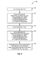
- FIG. 6 is a flow chart illustrating an image rejection calibration process according to another embodiment of the present invention.
- This embodiment is particularly beneficial for receivers, such as the receiver 22 of FIG. 2 , having a polyphase filter separating two stages of the receiver 22 and where the output of the receiver 22 is at an IF or VLIF such that image rejection calibration is also performed at IF or VLIF.
- the following discussion uses the receiver 22 of FIG. 2 as an example. However, it should be appreciated that this image rejection calibration process may be used for any quadrature receiver having two main stages separated by a polyphase filter.
- the digital IRC control circuitry 70 sets the polyphase notch filter 32 to a bypass mode (step 200 ).
- the IRC system 26 performs coarse error correction ( 202 ).
- the coarse error correction determines an amplitude and phase error of the receiver front-end 24 with the polyphase notch filter 32 bypassed and applies corresponding correction factors to the first stage 30 of the receiver front-end 24 .
- steps 200 and 202 are optional and may not be needed in some implementations.
- a substantially ideal quadrature test signal is applied to the input of the second stage 34 of the receiver front-end 24 .
- the amplitude and phase errors determined by the IRC system 26 during step 206 are estimates of the amplitude and phase errors of the second stage 34 of the receiver front-end 24 .
- FIG. 7 illustrates step 202 of FIG. 6 in more detail according to one embodiment of the present invention.
- the digital IRC control circuitry 70 sets the phase shift of the RF phase shifter 62 to zero degrees (step 300 ). Again, note that while phase shifts of 0 and 90 degrees are discussed herein, the RF phase shifter 62 may use any two phase shifts that are approximately 90 degrees apart.
- the digital IRC control circuitry 70 obtains a first amplitude (or gain) error estimate (GE 0 ) and a first phase error estimate (PE 0 ) based on measurements of a quadrature output signal (I R , Q R ) output by the receiver front-end 24 while a first test signal is applied to the RF input of the receiver front-end 24 by the IRC modulator 60 and the RF phase shifter 62 (step 302 ).
- GE 0 amplitude (or gain) error estimate
- PE 0 first phase error estimate
- the first amplitude error estimate (GE 0 ) is provided using the outputs of the master and slave CORDICs 94 and 96 based on equation (17) above, and the first phase error estimate (PE 0 ) is provided using the outputs of the master and slave CORDICs 94 and 96 using equation (20) above.
- the second amplitude error estimate (GE 90 ) is provided using the outputs of the master and slave CORDICs 94 and 96 based on equation (18) above, and the second phase error estimate (PE 90 ) is provided using the outputs of the master and slave CORDICs 94 and 96 using equation (21) above.
- the digital IRC control circuitry 70 determines an amplitude error (a R ) and a phase error ( ⁇ R ) of the receiver front-end 24 (step 308 ).
- the amplitude error (a R ) is determined using the first and second amplitude error estimates (GE 0 and GE 90 ) based on equation (19) above.
- the phase error ( ⁇ R ) may be determined using the first and second phase error estimates (PE 0 and PE 90 ) based on equation (22).
- FIG. 8 illustrates step 206 of FIG. 6 in more detail according to one embodiment of the present invention.
- the digital IRC control circuitry 70 sets the phase shift of the RF phase shifter 62 to 0 degrees (step 400 ). Again, note that while phase shifts of 0 and 90 degrees are discussed herein, the RF phase shifter 62 may use any two phase shifts that are approximately 90 degrees apart.
- the digital IRC control circuitry 70 obtains a first amplitude (or gain) error estimate (GE 0 ) and a first phase error estimate (PE 0 ) based on measurements of a quadrature output signal (I R , Q R ) output by the receiver front-end 24 while a first test signal is applied to the RF input of the receiver front-end 24 by the IRC modulator 60 and the RF phase shifter 62 (step 402 ).
- the test signals used for step 206 and, if desired, for steps 202 and 208 of FIG. 6 are provided such that the images of the test signals are within a high attenuation frequency zone of the polyphase notch filter 32 .
- the first amplitude error estimate (GE 0 ) is provided using the outputs of the master and slave CORDICs 94 and 96 based on equation (17) above, and the first phase error estimate (PE 0 ) is provided using the outputs of the master and slave CORDICs 94 and 96 using equation (20) above.
- the digital IRC control circuitry 70 sets the phase shift of the RF phase shifter 62 to 90 degrees (step 404 ). Once the RF phase shift is set to 90 degrees, the digital IRC control circuitry 70 obtains a second amplitude error estimate (GE 90 ) and a second phase error estimate (PE 90 ) based on measurements of the quadrature output signal (I R , Q R ) output by the receiver front-end 24 while a second test signal that is approximately 90 degrees out-of-phase with the first test signal is applied to the RF input of the receiver front-end 24 (step 406 ). Again, the test signals used for step 206 and, if desired, for steps 202 and 208 of FIG.
- GE 90 a second amplitude error estimate
- PE 90 phase error estimate
- the second amplitude error estimate (GE 90 ) is provided using the outputs of the master and slave CORDICs 94 and 96 based on equation (18) above, and the second phase error estimate (PE 90 ) is provided using the outputs of the master and slave CORDICs 94 and 96 using equation (21) above.
- the digital IRC control circuitry 70 determines an amplitude error (a R ) and a phase error ( ⁇ R ) of the receiver front-end 24 (step 408 ). More specifically, in this embodiment, the amplitude error (a R ) is determined using the first and second amplitude error estimates (GE 0 and GE 90 ) based on equation (19) above. Similarly, the phase error ( ⁇ R ) may be determined using the first and second phase error estimates (PE 0 and PE 90 ) based on equation (22).
- the resulting signals at the input of the second stage 34 of the receiver front-end 24 are substantially ideal quadrature signals.
- the amplitude error (a R ) and phase error ( ⁇ R ) determined in step 408 are substantially the amplitude error and phase error of the second stage 34 of the receiver front-end 24 .
- step 408 is optional. In some situations, step 408 may not be performed.
- the amplitude and phase error estimates (GE 0 , GE 90 , PE 0 , and PE 90 ) measured in steps 402 and 406 are stored for subsequent use in determining the amplitude and phase errors of the first stage 30 of the receiver front-end 24 . In this case, step 408 may not be performed unless, for example, it is also desirable to correct for the amplitude and phase errors of the second stage 34 .
- FIG. 9 illustrates step 210 of FIG. 6 in more detailed according to one embodiment of the present invention.
- the digital IRC control circuitry 70 sets the phase shift of the RF phase shifter 62 to zero degrees (step 500 ). Note that, as discussed above, the polyphase notch filter 32 is bypassed during step 210 of FIG. 6 .
- the digital IRC control circuitry 70 obtains a first amplitude (or gain) error estimate (GE 0 ) and a first phase error estimate (PE 0 ) based on measurements of a quadrature output signal (I R , Q R ) output by the receiver front-end 24 while a first test signal is applied to the RF input of the receiver front-end 24 by the IRC modulator 60 and the RF phase shifter 62 (step 502 ).
- GE 0 amplitude (or gain) error estimate
- PE 0 first phase error estimate
- the first amplitude error estimate (GE 0 ) is provided using the outputs of the master and slave CORDICs 94 and 96 based on equation (17) above, and the first phase error estimate (PE 0 ) is provided using the outputs of the master and slave CORDICs 94 and 96 using equation (20) above.
- the digital IRC control circuitry 70 sets the phase shift of the RF phase shifter 62 to 90 degrees (step 504 ). Once the RF phase shift is set to 90 degrees, the digital IRC control circuitry 70 obtains a second amplitude error estimate (GE 90 ) and a second phase error estimate (PE 90 ) based on measurements of the quadrature output signal (I R , Q R ) output by the receiver front-end 24 while a second test signal that is approximately 90 degrees out-of-phase with the first test signal is applied to the RF input of the receiver front-end 24 (step 506 ).
- GE 90 a second amplitude error estimate
- PE 90 phase error estimate
- the second amplitude error estimate (GE 90 ) is provided using the outputs of the master and slave CORDICs 94 and 96 based on equation (18) above, and the second phase error estimate (PE 90 ) is provided using the outputs of the master and slave CORDICs 94 and 96 using equation (21) above.
- the digital IRC control circuitry 70 determines an amplitude error (a R ) and a phase error ( ⁇ R ) of the first stage 30 of the receiver front-end 24 (step 508 ). More specifically, in this embodiment, the amplitude error (a R ) for the first stage 30 is determined based on the equation:
- phase error ( ⁇ R ) for the first stage 30 of the receiver front-end 24 may be determined based on the equation:
- the digital IRC control circuitry 70 applies corresponding correction factors to the first stage 30 (step 510 ).
- the digital IRC control circuitry 70 may apply correction factors for the amplitude and phase errors for the second stage 34 of the receiver front-end 24 in the second stage 34 , apply correction factors for the amplitude and phase errors of the second stage 34 to the digital processor 12 ( FIG. 1 ) for correction in the digital processor 12 , or provide the amplitude and phase errors of the second stage 34 to the digital processor 12 for correction.
Landscapes
- Engineering & Computer Science (AREA)
- Computer Networks & Wireless Communication (AREA)
- Signal Processing (AREA)
- Digital Transmission Methods That Use Modulated Carrier Waves (AREA)
Abstract
Description
X(t)=I(t)cos(ωc t)−Q(t)sin(ωc t), (1)
where ωc is the carrier frequency, t is time, and the weighting functions I(t) and Q(t) are the orthogonal components. In the
X T(t)=I T(t)cos(ωc t)−Q T(t)sin(ωc t); and (2)
X R(t)=I R(t)cos(ωc t+θ)−Q R(t)sin(ωc t+θ), (3)
where θ is a phase offset between the transmit and receive carriers ωc, which is unimportant in normal operation. For a non-ideal transceiver 10:
X T(t)=I′ T(t)cos(ωc t)−Q′ T(t)sin(ωc t); and (4)
X R(t)=I′ R(t)cos(ωc t+θ)−Q′ R(t)sin(ωc t+θ), (5)
where I′T and Q′T are the inputs to an ideal transmitter that would generate the same RF transmit signal (XT) as the
ε=a T −j(θT2−θT1); and (6)
α=2+a T +j(θT2+θT1). (7)
Note that these equations for c and a assume that the
I 0 =−je −jθ·ε+α for a phase shift of 0 degrees; (8)
Q 90 =−je jθ·ε+α for a phase shift of 90 degrees; (9)
I 90 =je jθ·ε+α for a phase shift of 90 degrees; and (10)
Q 0 =je −jθ·ε+α for a phase shift of 0 degrees. (11)
The measurements of the quadrature output signal output from the receiver front-
Similarly, the measurements of the quadrature output signal output from the receiver front-
where the function abs( ) returns an amplitude or magnitude of a complex term.
where GE0 is an amplitude error estimate for the test signal at a phase shift of 0 degrees and GE90 is an amplitude error estimate for the test signal at a phase shift of 90 degrees. Then, using equations (17) and (18), the amplitude error (aR) of the receiver front-
PE 0=ang(I R ·e −jωt|0)−ang(Q R ·e −jωt|0); and (20)
PE 90=ang(I R ·e −jωt|90)−ang(QR ·e −jωt|90) (21)
where PE0 is a phase error estimate for the test signal at a phase shift of 0 degrees and PE90 is a phase error estimate for the test signal at a phase shift of 90 degrees. The function ang( ) returns a phase of a complex term. Using equations (20) and (21), the phase error (θR) of the receiver front-
Similarly, the phase error (θR) for the
Claims (21)
Priority Applications (1)
| Application Number | Priority Date | Filing Date | Title |
|---|---|---|---|
| US12/371,018 US8064863B1 (en) | 2008-02-14 | 2009-02-13 | Image rejection calibration |
Applications Claiming Priority (2)
| Application Number | Priority Date | Filing Date | Title |
|---|---|---|---|
| US2859008P | 2008-02-14 | 2008-02-14 | |
| US12/371,018 US8064863B1 (en) | 2008-02-14 | 2009-02-13 | Image rejection calibration |
Publications (1)
| Publication Number | Publication Date |
|---|---|
| US8064863B1 true US8064863B1 (en) | 2011-11-22 |
Family
ID=44936855
Family Applications (1)
| Application Number | Title | Priority Date | Filing Date |
|---|---|---|---|
| US12/371,018 Active 2030-05-14 US8064863B1 (en) | 2008-02-14 | 2009-02-13 | Image rejection calibration |
Country Status (1)
| Country | Link |
|---|---|
| US (1) | US8064863B1 (en) |
Cited By (5)
| Publication number | Priority date | Publication date | Assignee | Title |
|---|---|---|---|---|
| US20110292290A1 (en) * | 2010-05-26 | 2011-12-01 | Seiko Epson Corporation | Frequency conversion circuit, frequency conversion method, and electronic apparatus |
| US9042500B1 (en) * | 2013-12-17 | 2015-05-26 | Motorola Solutions, Inc. | Very low intermediate frequency (VLIF) receiver and method of controlling a VLIF receiver |
| US9319027B1 (en) * | 2014-12-17 | 2016-04-19 | Silicon Laboratories Inc. | Injecting a tone for image rejection calibration |
| US20160315646A1 (en) * | 2015-04-23 | 2016-10-27 | Nxp B.V. | Wireless receiver and method |
| US11190285B1 (en) * | 2020-11-09 | 2021-11-30 | Hangzhou Geo-Chip Technology Co., Ltd. | Transmitter, receiver, signal transceiver and methods therefor |
Citations (5)
| Publication number | Priority date | Publication date | Assignee | Title |
|---|---|---|---|---|
| US20070080835A1 (en) * | 2005-10-07 | 2007-04-12 | Koji Maeda | Receiver |
| US7299021B2 (en) * | 2001-12-28 | 2007-11-20 | Nokia Corporation | Method and apparatus for scaling the dynamic range of a receiver for continuously optimizing performance versus power consumption |
| US7477881B2 (en) * | 2004-08-13 | 2009-01-13 | Samsung Electronics Co., Ltd. | Intermediate frequency receiver with improved image rejection ratio |
| US7580680B2 (en) * | 2005-06-08 | 2009-08-25 | Intel Corporation | Method of reducing imbalance in a quadrature frequency converter, method of measuring imbalance in such a converter, and apparatus for performing such method |
| US7636588B2 (en) * | 2003-03-04 | 2009-12-22 | Samsung Electronics Co., Ltd. | Method for saving power in a wireless telephone |
-
2009
- 2009-02-13 US US12/371,018 patent/US8064863B1/en active Active
Patent Citations (5)
| Publication number | Priority date | Publication date | Assignee | Title |
|---|---|---|---|---|
| US7299021B2 (en) * | 2001-12-28 | 2007-11-20 | Nokia Corporation | Method and apparatus for scaling the dynamic range of a receiver for continuously optimizing performance versus power consumption |
| US7636588B2 (en) * | 2003-03-04 | 2009-12-22 | Samsung Electronics Co., Ltd. | Method for saving power in a wireless telephone |
| US7477881B2 (en) * | 2004-08-13 | 2009-01-13 | Samsung Electronics Co., Ltd. | Intermediate frequency receiver with improved image rejection ratio |
| US7580680B2 (en) * | 2005-06-08 | 2009-08-25 | Intel Corporation | Method of reducing imbalance in a quadrature frequency converter, method of measuring imbalance in such a converter, and apparatus for performing such method |
| US20070080835A1 (en) * | 2005-10-07 | 2007-04-12 | Koji Maeda | Receiver |
Cited By (9)
| Publication number | Priority date | Publication date | Assignee | Title |
|---|---|---|---|---|
| US20110292290A1 (en) * | 2010-05-26 | 2011-12-01 | Seiko Epson Corporation | Frequency conversion circuit, frequency conversion method, and electronic apparatus |
| US9042500B1 (en) * | 2013-12-17 | 2015-05-26 | Motorola Solutions, Inc. | Very low intermediate frequency (VLIF) receiver and method of controlling a VLIF receiver |
| US20150171906A1 (en) * | 2013-12-17 | 2015-06-18 | Motorola Solutions, Inc | Very low intermediate frequency (vlif) receiver and method of controlling a vlif receiver |
| US9319027B1 (en) * | 2014-12-17 | 2016-04-19 | Silicon Laboratories Inc. | Injecting a tone for image rejection calibration |
| US20160315646A1 (en) * | 2015-04-23 | 2016-10-27 | Nxp B.V. | Wireless receiver and method |
| US9705544B2 (en) * | 2015-04-23 | 2017-07-11 | Nxp B.V. | Wireless receiver and method |
| US11190285B1 (en) * | 2020-11-09 | 2021-11-30 | Hangzhou Geo-Chip Technology Co., Ltd. | Transmitter, receiver, signal transceiver and methods therefor |
| CN114531164A (en) * | 2020-11-09 | 2022-05-24 | 杭州地芯科技有限公司 | Transmitter, receiver and signal transceiver and corresponding method thereof |
| CN114531164B (en) * | 2020-11-09 | 2023-12-29 | 杭州地芯科技有限公司 | Transmitter, receiver, signal transceiver and corresponding methods |
Similar Documents
| Publication | Publication Date | Title |
|---|---|---|
| US7856050B1 (en) | Receiver and transmitter calibration to compensate for frequency dependent I/Q imbalance | |
| US7346325B2 (en) | Receiver, receiving method and portable wireless apparatus | |
| US7782928B2 (en) | Method and apparatus for self-calibration in a mobile transceiver | |
| US7995645B2 (en) | Apparatus for measuring in-phase and quadrature (IQ) imbalance | |
| US7925217B2 (en) | Receiving circuit and method for compensating IQ mismatch | |
| US7376170B2 (en) | Digital imbalance correction method and device in a receiver for multi-carrier applications | |
| US8018990B2 (en) | Apparatus for measuring in-phase and quadrature (IQ) imbalance | |
| US8093943B2 (en) | Phase noise correction device and its method | |
| US9413294B2 (en) | Apparatus and method for correcting IQ imbalance | |
| US20040137869A1 (en) | Direct conversion receiver for calibrating phase and gain mismatch | |
| US20170257176A1 (en) | Method and device for calibrating iq imbalance and dc offset of rf tranceiver | |
| US6516186B1 (en) | Image-rejection receiver | |
| US9385656B2 (en) | Low complexity frequency selective IQ mismatch digital RX balancer and TX inverse balancer for non-ideal RF front-end | |
| US8064863B1 (en) | Image rejection calibration | |
| US20050152481A1 (en) | Method and apparatus of iq mismatch calibration | |
| US20090028231A1 (en) | Apparatus for measuring iq imbalance | |
| US7450919B1 (en) | I/Q mismatch correction using transmitter leakage and gain modulation | |
| US20080166978A1 (en) | Method and circuit for estimating in-phase/quadrature signal amplitude imbalance | |
| EP1916764B1 (en) | Method and apparatus for compensating for mismatch occurring in radio frequency quadrature transceiver | |
| US10225118B1 (en) | Carrier leakage correction method for quadrature modulator | |
| US8526533B2 (en) | Systems and methods for measuring I-Q mismatch | |
| EP0875988B1 (en) | Interference suppression in RF signals | |
| CN110535575B (en) | Method for calculating and compensating I/Q signal linear phase imbalance | |
| US20050047528A1 (en) | Direct conversion receiver and receiving method | |
| CN101390360A (en) | In phase and quadrature path imbalance compensation |
Legal Events
| Date | Code | Title | Description |
|---|---|---|---|
| AS | Assignment |
Owner name: RF MICRO DEVICES, INC., NORTH CAROLINA Free format text: ASSIGNMENT OF ASSIGNORS INTEREST;ASSIGNORS:REED, DAVID;KHLAT, NADIM;SIGNING DATES FROM 20090210 TO 20090310;REEL/FRAME:022438/0145 |
|
| STCF | Information on status: patent grant |
Free format text: PATENTED CASE |
|
| AS | Assignment |
Owner name: BANK OF AMERICA, N.A., AS ADMINISTRATIVE AGENT, TE Free format text: NOTICE OF GRANT OF SECURITY INTEREST IN PATENTS;ASSIGNOR:RF MICRO DEVICES, INC.;REEL/FRAME:030045/0831 Effective date: 20130319 |
|
| FPAY | Fee payment |
Year of fee payment: 4 |
|
| AS | Assignment |
Owner name: RF MICRO DEVICES, INC., NORTH CAROLINA Free format text: TERMINATION AND RELEASE OF SECURITY INTEREST IN PATENTS (RECORDED 3/19/13 AT REEL/FRAME 030045/0831);ASSIGNOR:BANK OF AMERICA, N.A., AS ADMINISTRATIVE AGENT;REEL/FRAME:035334/0363 Effective date: 20150326 |
|
| AS | Assignment |
Owner name: QORVO US, INC., NORTH CAROLINA Free format text: MERGER;ASSIGNOR:RF MICRO DEVICES, INC.;REEL/FRAME:039196/0941 Effective date: 20160330 |
|
| FEPP | Fee payment procedure |
Free format text: MAINTENANCE FEE REMINDER MAILED (ORIGINAL EVENT CODE: REM.); ENTITY STATUS OF PATENT OWNER: LARGE ENTITY |
|
| FEPP | Fee payment procedure |
Free format text: 7.5 YR SURCHARGE - LATE PMT W/IN 6 MO, LARGE ENTITY (ORIGINAL EVENT CODE: M1555); ENTITY STATUS OF PATENT OWNER: LARGE ENTITY |
|
| MAFP | Maintenance fee payment |
Free format text: PAYMENT OF MAINTENANCE FEE, 8TH YEAR, LARGE ENTITY (ORIGINAL EVENT CODE: M1552); ENTITY STATUS OF PATENT OWNER: LARGE ENTITY Year of fee payment: 8 |
|
| MAFP | Maintenance fee payment |
Free format text: PAYMENT OF MAINTENANCE FEE, 12TH YEAR, LARGE ENTITY (ORIGINAL EVENT CODE: M1553); ENTITY STATUS OF PATENT OWNER: LARGE ENTITY Year of fee payment: 12 |