US8063496B2 - Semiconductor integrated circuit device and method of fabricating the same - Google Patents
Semiconductor integrated circuit device and method of fabricating the same Download PDFInfo
- Publication number
- US8063496B2 US8063496B2 US12/230,429 US23042908A US8063496B2 US 8063496 B2 US8063496 B2 US 8063496B2 US 23042908 A US23042908 A US 23042908A US 8063496 B2 US8063496 B2 US 8063496B2
- Authority
- US
- United States
- Prior art keywords
- pad
- semiconductor substrate
- redistribution
- layer
- integrated circuit
- Prior art date
- Legal status (The legal status is an assumption and is not a legal conclusion. Google has not performed a legal analysis and makes no representation as to the accuracy of the status listed.)
- Active, expires
Links
Images


Classifications
-
- H—ELECTRICITY
- H10—SEMICONDUCTOR DEVICES; ELECTRIC SOLID-STATE DEVICES NOT OTHERWISE PROVIDED FOR
- H10P—GENERIC PROCESSES OR APPARATUS FOR THE MANUFACTURE OR TREATMENT OF DEVICES COVERED BY CLASS H10
- H10P14/00—Formation of materials, e.g. in the shape of layers or pillars
- H10P14/40—Formation of materials, e.g. in the shape of layers or pillars of conductive or resistive materials
-
- H—ELECTRICITY
- H10—SEMICONDUCTOR DEVICES; ELECTRIC SOLID-STATE DEVICES NOT OTHERWISE PROVIDED FOR
- H10W—GENERIC PACKAGES, INTERCONNECTIONS, CONNECTORS OR OTHER CONSTRUCTIONAL DETAILS OF DEVICES COVERED BY CLASS H10
- H10W20/00—Interconnections in chips, wafers or substrates
- H10W20/20—Interconnections within wafers or substrates, e.g. through-silicon vias [TSV]
-
- H—ELECTRICITY
- H10—SEMICONDUCTOR DEVICES; ELECTRIC SOLID-STATE DEVICES NOT OTHERWISE PROVIDED FOR
- H10W—GENERIC PACKAGES, INTERCONNECTIONS, CONNECTORS OR OTHER CONSTRUCTIONAL DETAILS OF DEVICES COVERED BY CLASS H10
- H10W20/00—Interconnections in chips, wafers or substrates
- H10W20/01—Manufacture or treatment
- H10W20/021—Manufacture or treatment of interconnections within wafers or substrates
- H10W20/023—Manufacture or treatment of interconnections within wafers or substrates the interconnections being through-semiconductor vias
- H10W20/0234—Manufacture or treatment of interconnections within wafers or substrates the interconnections being through-semiconductor vias comprising etching via holes that stop on pads or on electrodes
-
- H—ELECTRICITY
- H10—SEMICONDUCTOR DEVICES; ELECTRIC SOLID-STATE DEVICES NOT OTHERWISE PROVIDED FOR
- H10W—GENERIC PACKAGES, INTERCONNECTIONS, CONNECTORS OR OTHER CONSTRUCTIONAL DETAILS OF DEVICES COVERED BY CLASS H10
- H10W20/00—Interconnections in chips, wafers or substrates
- H10W20/01—Manufacture or treatment
- H10W20/021—Manufacture or treatment of interconnections within wafers or substrates
- H10W20/023—Manufacture or treatment of interconnections within wafers or substrates the interconnections being through-semiconductor vias
- H10W20/0242—Manufacture or treatment of interconnections within wafers or substrates the interconnections being through-semiconductor vias comprising etching via holes from the back sides of the chips, wafers or substrates
-
- H—ELECTRICITY
- H10—SEMICONDUCTOR DEVICES; ELECTRIC SOLID-STATE DEVICES NOT OTHERWISE PROVIDED FOR
- H10W—GENERIC PACKAGES, INTERCONNECTIONS, CONNECTORS OR OTHER CONSTRUCTIONAL DETAILS OF DEVICES COVERED BY CLASS H10
- H10W20/00—Interconnections in chips, wafers or substrates
- H10W20/20—Interconnections within wafers or substrates, e.g. through-silicon vias [TSV]
- H10W20/211—Through-semiconductor vias, e.g. TSVs
- H10W20/216—Through-semiconductor vias, e.g. TSVs characterised by dielectric material at least partially filling the via holes, e.g. covering the through-semiconductor vias in the via holes
-
- H—ELECTRICITY
- H10—SEMICONDUCTOR DEVICES; ELECTRIC SOLID-STATE DEVICES NOT OTHERWISE PROVIDED FOR
- H10W—GENERIC PACKAGES, INTERCONNECTIONS, CONNECTORS OR OTHER CONSTRUCTIONAL DETAILS OF DEVICES COVERED BY CLASS H10
- H10W20/00—Interconnections in chips, wafers or substrates
- H10W20/20—Interconnections within wafers or substrates, e.g. through-silicon vias [TSV]
- H10W20/211—Through-semiconductor vias, e.g. TSVs
- H10W20/217—Through-semiconductor vias, e.g. TSVs comprising ring-shaped isolation structures outside of the via holes
-
- H—ELECTRICITY
- H10—SEMICONDUCTOR DEVICES; ELECTRIC SOLID-STATE DEVICES NOT OTHERWISE PROVIDED FOR
- H10W—GENERIC PACKAGES, INTERCONNECTIONS, CONNECTORS OR OTHER CONSTRUCTIONAL DETAILS OF DEVICES COVERED BY CLASS H10
- H10W72/00—Interconnections or connectors in packages
- H10W72/01—Manufacture or treatment
- H10W72/012—Manufacture or treatment of bump connectors, dummy bumps or thermal bumps
-
- H—ELECTRICITY
- H10—SEMICONDUCTOR DEVICES; ELECTRIC SOLID-STATE DEVICES NOT OTHERWISE PROVIDED FOR
- H10D—INORGANIC ELECTRIC SEMICONDUCTOR DEVICES
- H10D30/00—Field-effect transistors [FET]
- H10D30/60—Insulated-gate field-effect transistors [IGFET]
-
- H—ELECTRICITY
- H10—SEMICONDUCTOR DEVICES; ELECTRIC SOLID-STATE DEVICES NOT OTHERWISE PROVIDED FOR
- H10W—GENERIC PACKAGES, INTERCONNECTIONS, CONNECTORS OR OTHER CONSTRUCTIONAL DETAILS OF DEVICES COVERED BY CLASS H10
- H10W70/00—Package substrates; Interposers; Redistribution layers [RDL]
- H10W70/01—Manufacture or treatment
- H10W70/05—Manufacture or treatment of insulating or insulated package substrates, or of interposers, or of redistribution layers
-
- H—ELECTRICITY
- H10—SEMICONDUCTOR DEVICES; ELECTRIC SOLID-STATE DEVICES NOT OTHERWISE PROVIDED FOR
- H10W—GENERIC PACKAGES, INTERCONNECTIONS, CONNECTORS OR OTHER CONSTRUCTIONAL DETAILS OF DEVICES COVERED BY CLASS H10
- H10W72/00—Interconnections or connectors in packages
- H10W72/20—Bump connectors, e.g. solder bumps or copper pillars; Dummy bumps; Thermal bumps
- H10W72/241—Dispositions, e.g. layouts
- H10W72/244—Dispositions, e.g. layouts relative to underlying supporting features, e.g. bond pads, RDLs or vias
-
- H—ELECTRICITY
- H10—SEMICONDUCTOR DEVICES; ELECTRIC SOLID-STATE DEVICES NOT OTHERWISE PROVIDED FOR
- H10W—GENERIC PACKAGES, INTERCONNECTIONS, CONNECTORS OR OTHER CONSTRUCTIONAL DETAILS OF DEVICES COVERED BY CLASS H10
- H10W72/00—Interconnections or connectors in packages
- H10W72/20—Bump connectors, e.g. solder bumps or copper pillars; Dummy bumps; Thermal bumps
- H10W72/251—Materials
- H10W72/252—Materials comprising solid metals or solid metalloids, e.g. PbSn, Ag or Cu
-
- H—ELECTRICITY
- H10—SEMICONDUCTOR DEVICES; ELECTRIC SOLID-STATE DEVICES NOT OTHERWISE PROVIDED FOR
- H10W—GENERIC PACKAGES, INTERCONNECTIONS, CONNECTORS OR OTHER CONSTRUCTIONAL DETAILS OF DEVICES COVERED BY CLASS H10
- H10W72/00—Interconnections or connectors in packages
- H10W72/20—Bump connectors, e.g. solder bumps or copper pillars; Dummy bumps; Thermal bumps
- H10W72/29—Bond pads specially adapted therefor
-
- H—ELECTRICITY
- H10—SEMICONDUCTOR DEVICES; ELECTRIC SOLID-STATE DEVICES NOT OTHERWISE PROVIDED FOR
- H10W—GENERIC PACKAGES, INTERCONNECTIONS, CONNECTORS OR OTHER CONSTRUCTIONAL DETAILS OF DEVICES COVERED BY CLASS H10
- H10W72/00—Interconnections or connectors in packages
- H10W72/90—Bond pads, in general
- H10W72/931—Shapes of bond pads
- H10W72/932—Plan-view shape, i.e. in top view
Definitions
- Embodiments of the present invention relate to a semiconductor integrated circuit device and a method of fabricating the same. More particularly, embodiments of the present invention relate to a semiconductor integrated circuit device with a simplified structure and a method of fabricating the same.
- semiconductor package technology has evolved from, e.g., a dual in line package (DIP), a small outline with J-lead (SOJ), and a quad flat package (QFP), into, e.g., a ball grid array (BGA) and a chip scale package (CSP).
- DIP dual in line package
- SOJ small outline with J-lead
- QFP quad flat package
- BGA ball grid array
- CSP chip scale package
- SiP system in package
- SiP package in package
- FCS-CSP flip chip stacked-CSP
- Package technology refers to implementation of a three-dimensional package structure of a system at a package level.
- the conventional implementation of package technology may include use of stack technology, embedded technology for embedding active and passive devices with chips, and through silicon via (TSV) technology.
- TSV through silicon via
- the TSV technology may connect individual parts or chips to each other using thousands of micro-wires to facilitate signal exchange therebetween.
- the conventional TSV technology may include forming hole patterns on a semiconductor substrate in order to form micro-wires and forming an insulation film in order to electrically isolate the micro-wires from the semiconductor substrate.
- the number of required processes in the conventional TLV may be large, so production of a semiconductor integrated circuit device may be complicated. Further, the large number of processes in the conventional TLV may increase production costs of the semiconductor integrated circuit device, while reducing processing efficiency thereof. Consequently, productivity of the semiconductor integrated circuit device may be reduced.
- Embodiments of the present invention are therefore directed to a semiconductor integrated circuit device and a method of fabricating the same, which substantially overcome one or more of the disadvantages of the related art.
- a semiconductor integrated circuit device including a semiconductor substrate having a main chip region and a pad region, a multi-layer pad structure on the pad region of the semiconductor substrate, a redistribution pad through the semiconductor substrate and in contact with a bottom surface of the multi-layer pad structure, the redistribution pad being electrically connected to the multi-layer pad structure, a trench belt through the semiconductor substrate and surrounding the redistribution pad, the trench belt electrically isolating the redistribution pad and a portion of the semiconductor substrate adjacent to the redistribution pad, and a connection terminal on the redistribution pad, the connection terminal electrically connecting the redistribution pad to an external source.
- the multi-layer pad structure may include a conductive material, the multi-layer pad structure being a stacked structure of a contact, a plurality of lines, and a plurality of vias connecting the lines to one other.
- the semiconductor integrated circuit device may further include a plurality of multi-layer pad structures on the pad region of the semiconductor substrate, the redistribution pad being electrically connected to each of the multi-layer pad structures.
- the semiconductor integrated circuit device may further include a pad contact hole through the semiconductor substrate, the pad contact hole exposing the bottom surface of the multi-layer pad structure, and the redistribution pad being on a portion of a bottom surface of the semiconductor substrate and on sidewalls of the pad contact hole.
- a depth of the trench belt may be greater than a thickness of the semiconductor substrate.
- the semiconductor integrated circuit device may further include a passivation film on a bottom surface of the semiconductor substrate to bury the trench belt, the connection terminal being configured through the passivation film.
- a semiconductor integrated circuit device including a semiconductor substrate having a main chip region and a pad region, a plurality of inter-layer insulation films on the semiconductor substrate, a multi-layer pad structure on the semiconductor substrate, the multi-layer pad structure penetrating through the inter-layer insulation films in the pad region of the semiconductor substrate, a pad contact hole through the semiconductor substrate, the pad contact hole exposing a bottom surface of the multi-layer pad structure, a redistribution pad in the pad contact hole and on portions of a bottom surface of the semiconductor substrate, the redistribution pad being electrically connected to the multi-layer pad structure, a trench belt through the semiconductor substrate and surrounding the redistribution pad, the trench belt electrically isolating the redistribution pad and a portion of the semiconductor substrate adjacent to the redistribution pad, a passivation film on the bottom surface of the semiconductor substrate and on the redistribution pad, the passivation film burying the trench belt and the pad
- the multi-layer pad structure may be a stacked structure of a contact, a plurality of lines, and a plurality of vias connecting the lines to one other.
- the connection terminal may be a solder ball.
- the pad region of the semiconductor substrate may include a plurality of multi-layer pad structures, the redistribution pad being electrically connected to each of the multi-layer pad structures. A depth of the trench belt is greater than a thickness of the semiconductor substrate.
- At least one of the above and other features and advantages of the present invention may be also realized by providing a method of fabricating a semiconductor integrated circuit device, including forming a multi-layer pad structure on a pad region of a semiconductor substrate, forming a redistribution pad through the semiconductor substrate and in contact with a bottom surface of the multi-layer pad structure, the redistribution pad being electrically connected to the multi-layer pad structure, forming a trench belt through the semiconductor substrate and surrounding the redistribution pad, the trench belt electrically isolating the redistribution pad and a portion of the semiconductor substrate adjacent to the redistribution pad, and forming a connection terminal on the redistribution pad and electrically connecting the redistribution pad to the outside.
- Forming the multi-layer pad structure may include forming an integrated circuit structure with a plurality of contacts, a plurality of lines, and a plurality of vias connecting the lines to one another.
- Forming the redistribution pad may include forming a pad contact hole through the semiconductor substrate, the pad contact hole exposing the bottom surface of the multi-layer pad structure, and conformally forming the redistribution pad in the pad contact hole and on portions of a bottom surface of the semiconductor substrate.
- the method may further include a plurality of multi-layer pad structures on the semiconductor substrate, such that the redistribution pad is electrically connected to each of the multi-layer pad structures.
- Forming the trench belt may include over-etching the semiconductor substrate, such that a depth of the trench belt is greater than a thickness of the semiconductor substrate.
- Forming the trench belt may include separating the trench belt from the pad contact hole by a predetermined distance.
- Forming the redistribution pad may include electro-plating a redistribution pad seed layer.
- the method may further include forming a passivation film on the bottom surface of the semiconductor substrate and on the redistribution pad, such that the trench belt is buried.
- the connection terminal may be formed through the passivation film, a portion of the connection terminal being exposed to an outside through the passivation film.
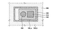
- FIG. 1 illustrates a schematic, top view of a wafer including a plurality of semiconductor integrated circuit devices according to an exemplary embodiment of the present invention
- FIG. 2 illustrates an enlarged, top view of a semiconductor integrated circuit device in portion A of FIG. 1 ;
- FIG. 3 illustrates a cross-sectional view along line III-III′ of FIG. 2 ;
- FIG. 4 illustrates a schematic, bottom view of a pad region of the semiconductor integrated circuit device of FIG. 3 ;
- FIG. 5 illustrates a schematic, bottom view of a pad region of a semiconductor integrated circuit device according to another exemplary embodiment of the present invention
- FIGS. 6A-10B illustrate sequential cross-sectional and bottom views of stages in a method of fabricating a semiconductor integrated circuit device according to an exemplary embodiment of the present invention.
- FIGS. 11-13 illustrate sequential cross-sectional and bottom views of stages in a method of fabricating a semiconductor integrated circuit device according to another exemplary embodiment of the present invention.
- each of the expressions “at least one,” “one or more,” and “and/or” are open-ended expressions that are both conjunctive and disjunctive in operation.
- each of the expressions “at least one of A, B, and C,” “at least one of A, B, or C,” “one or more of A, B, and C,” “one or more of A, B, or C” and “A, B, and/or C” includes the following meanings: A alone; B alone; C alone; both A and B together; both A and C together; both B and C together; and all three of A, B, and C together.
- Embodiments of the invention are described herein with reference to plan and cross-section illustrations of idealized embodiments of the invention. As such, variations from the structures illustrated in the drawing figures, e.g., due to manufacturing techniques and/or tolerances, are to be expected. Accordingly, embodiments of the invention should not be construed as limited to the particular shapes of regions illustrated herein but are to include deviations in shapes that result, for example, from manufacturing. Thus, the regions illustrated in the figures are schematic in nature and their shapes are not intended to illustrate the actual shape of a region of a device and are not intended to limit the scope of the invention.
- FIG. 1 illustrates a top view of a wafer 1 including a plurality of semiconductor integrated circuit devices C 1 through C 3 according to an exemplary embodiment of the present invention.
- FIG. 2 illustrates an enlarged view of portion A of FIG. 1 for explaining a semiconductor integrated circuit device 10 according to an exemplary embodiment of the present invention.
- FIG. 3 illustrates a cross-sectional view of the semiconductor integrated circuit device 10 taken along line III-III′ of FIG. 2 .
- FIG. 4 illustrates a bottom view of a pad region PR of the semiconductor integrated circuit device 10 in FIG. 3 .
- the wafer 1 may include a plurality of semiconductor integrated circuit devices, e.g., semiconductor integrated circuit devices C 1 through C 3 , divided by scribe lines SL.
- the semiconductor integrated circuit devices C 1 through C 3 may be semiconductor integrated circuit devices of a substantially same type, e.g., memory chips, or may be semiconductor integrated circuit devices of different types for performing different operation to complete one function, e.g., a memory chip, an application-specific integrated circuit (ASIC) chip, and a processor.
- ASIC application-specific integrated circuit
- embodiments of the present invention may be applied not only to a single semiconductor integrated circuit device, e.g., the semiconductor integrated circuit device 10 in portion A, but also to a M ⁇ N array chip of semiconductor integrated circuit devices required to form one module, e.g., a 2 ⁇ 3 array chip B.
- the semiconductor integrated circuit device 10 may include a semiconductor substrate 100 having a main chip region CR and the pad region PR.
- a multi-layer pad structure 310 , a redistribution pad 340 , a connection terminal 350 , a trench belt 330 , and a passivation film 360 may be formed on the pad region PR.
- An integrated circuit structure 20 may be formed on the main chip region CR.
- the semiconductor substrate 100 may be a silicon semiconductor substrate, a silicon on insulator (SOI) semiconductor substrate, a gallium arsenic semiconductor substrate, a silicon germanium semiconductor substrate, a ceramic semiconductor substrate, a quartz semiconductor substrate, or a display glass semiconductor substrate.
- the semiconductor substrate 100 may be a P-type semiconductor substrate.
- a P-type epitaxial layer (not shown) may be grown on the semiconductor substrate 100 .
- the semiconductor substrate 100 may include the main chip region CR and the pad region PR surrounding the main chip region CR, as illustrated in FIG. 2 .
- the integrated circuit structure 20 of the semiconductor integrated circuit device 10 may be formed on the main chip region CR of the semiconductor substrate 100 , and devices electrically connecting the integrated circuit structure 20 to the outside may be formed on the pad region PR. It is noted, however, that other configurations of the pad region PR with respect to the main chip region CR region according to a type and characteristics of the semiconductor integrated circuit device 10 are within the scope of the present invention.
- the integrated circuit structure 20 of the semiconductor integrated circuit device 10 may have any suitable structure.
- An exemplary structure of the integrated circuit structure 20 of the semiconductor integrated circuit device 10 may be as follows.
- a device isolation region 201 may be formed on the semiconductor substrate 100 in the main chip region CR to define an active region.
- the device isolation region 201 may be, e.g., a field oxide (FOX) or a shallow trench isolation (STI) region, formed, e.g., by a local oxidation of silicon (LOCOS) method.
- a transistor including a gate insulation film 211 , a gate electrode 212 , a spacer 213 , and a source/drain region 202 may be formed in the main chip region CR.
- the gate insulation film 211 may be formed in the main chip region CR on the semiconductor substrate 100 , and the gate electrode 212 made of, e.g., polycrystalline silicon, may be formed on the gate insulation film 211 .
- the spacer 213 may be formed on both sidewalls of the gate electrode 212 , and the source/drain region 202 may be formed by ion-implanting impurities using the gate electrode 212 with the spacer 213 as an ion implantation mask.
- a self-aligned contact 214 may be formed on a region of the semiconductor substrate 100 .
- the self-aligned contact 214 may be formed on a portion of the main chip region CR to contact the source/drain region 202 , e.g., the self-aligned contact 214 may overlap a portion of the active region of the integrated circuit structure 20 .
- a first inter-layer insulation film 110 may be formed on a portion of the semiconductor substrate 100 not including the self-aligned contact 214 .
- the first inter-layer insulation film 110 may be in the pad region PR and in a portion of the main chip region CR, e.g., the first inter-layer insulation film 110 may overlap the device isolation region 201 .
- the first inter-layer insulation film 110 may include an insulating material, e.g., one or more of a flowable oxide (FOX) film, a tonen silazene (TOSZ) film, an undoped silicate glass (USG) film, a borosilicate glass (BSG) film, a phosphosilicate glass (PSG) film, a borophosphosilicate glass (BPSG) film, a plasma enhanced-tetra ethyl ortho silicate (PE-TEOS) film, a fluoride silicate glass (FSG) film, and/or a high density plasma film.
- a flowable oxide (FOX) film e.g., a flowable oxide (FOX) film, a tonen silazene (TOSZ) film, an undoped silicate glass (USG) film, a borosilicate glass (BSG) film, a phosphosilicate glass (PSG) film, a borophosphosilicate glass (BP
- a second inter-layer insulation film 120 may be formed on the semiconductor substrate 100 , e.g., on the first inter-layer insulation film 110 and on the self-aligned contact 214 .
- the second inter-layer insulation film 120 may include a bitline contact 221 , and a bitline 222 may be formed on a portion of the second inter-layer insulation film 120 .
- the bitline contact 221 may electrically connect the self-aligned contact 214 to the bitline 222 , and may be formed of a conductive material, e.g., tungsten (W) or tungsten alloy.
- the bitline 222 may overlap the self-aligned contact 214 , and may be formed of, e.g., ruthenium (Ru), rhodium (Rh), osmium (Os), palladium (Pd), platinum (Pt), tungsten (W), molybdenum (Mo), titanium (Ti), tantalum (Ta), aluminum (Al), copper (Cu), hafnium (Hf), zirconium (Zr), iridium (Ir), tungsten nitride (WN), molybdenum-nitride (MoN), titanium nitride (TiN), tantalum nitride (TaN), aluminum nitride (AlN), hafnium nitride (HfN), zirconium nitride (ZrN), tantalum silicon nitride (TaSiN), ruthenium oxide (RuO 2 ), iridium oxide (IrO 2
- a third inter-layer insulation film 130 may be formed on the second inter-layer insulation film 120 to cover the bitline contact 221 and the bitline 222 , i.e., the bitline 222 may be between the second and third inter-layer insulating films 120 and 130 .
- a storage electrode contact 231 may be formed through the second and third inter-layer insulation films 120 and 130 to electrically connect a storage electrode 241 to the self-aligned contact 214 .
- the storage electrode contact 231 may be formed of a conductive material, e.g., polycrystalline silicon.
- the storage electrode 241 may be formed on the third inter-layer insulation film 130 , and may have a cylindrical shape in order to enhance integration density and capacitance.
- the storage electrode 241 may be formed of a conductive material, e.g., polycrystalline silicon, and/or of a metal material, e.g., Ru, Rh, Os, Pd, Pt, W, Mo, Ti, Ta, Al, Cu, Hf, Zr, Ir, WN, MoN, TiN, TaN, AlN, HfN, ZrN, TaSiN, RuO 2 , IrO 2 , or a combination of the same.
- the storage electrode 241 may also have a stacked structure of metal and polycrystalline silicon.
- a dielectric film 242 may be conformally formed on the storage electrode 241 and along a profile of the storage electrode 241 .
- the dielectric film 242 may be formed of a dielectric material having a high dielectric constant (high-k), so that a desired capacitance can be achieved even when the size of the storage electrode 241 is reduced.
- the dielectric film 242 may be formed of HfO 2 , HfSiO, HfAlO, ZrO 2 , ZrSiO, ZrAlO, Ta 2 O 5 , TiO 2 , Al 2 O 3 , Nb 2 O 5 , CeO 2 , Y 2 O 3 , InO 3 , IrO 2 , SrTiO 3 , PbTiO 3 , SrRuO 3 , CaRuO 3 , (BaSr)TiO 3 , Pb(Zr,Ti) O 3 , (Pb,La)(Zr,Ti)O 3 , (Sr,Ca)RuO 3 , or a stack, e.g., a laminate structure, thereof.
- the dielectric film 242 may be a stacked layer having high dielectric constant, e.g., Oxide-Nitride-Oxide (ONO).
- a plate electrode 243 may be formed on each storage electrode 241 , such that the dielectric film 242 may be formed between the plate electrode 243 and the storage electrode 241 .
- the plate electrode 243 may be formed of a substantially same conductive material as the storage electrode 241 .
- the plate electrode 243 may be formed of polycrystalline silicon and/or a metal material.
- a fourth inter-layer insulation film 140 may be formed on the third inter-layer insulation film 130 on which the plate electrode 243 is formed.
- the integrated circuit structure 20 formed on the main chip region CR of the semiconductor integrated circuit device 10 has been described above.
- other configurations of the integrated circuit structure 20 e.g., additional inter-layer insulation films may be formed on the fourth inter-layer insulation film 140 , in accordance with a purpose of semiconductor integrated circuit device 10 , are within the scope of the present invention.
- the integrated circuit structure 20 formed on the main chip region CR may be changed in various forms by a person of ordinary skill in the art.
- the multi-layer pad structure 310 , the redistribution pad 340 , the connection terminal 350 , and the trench belt 330 may be formed in the pad region PR of the semiconductor substrate 100 .
- the multi-layer pad structure 310 may be connected to the integrated circuit structure 20 via an inner line (not shown) and to an external source (not shown) via the redistribution pad 340 and the connection terminal 350 . Accordingly, the multi-layer pad structure 310 may facilitate signal transmission of the semiconductor integrated circuit device 10 .
- the multi-layer pad structure 310 may extend through the first to fourth inter-layer insulation films 110 to 140 to contact the semiconductor substrate 100 .
- the multi-layer pad structure 310 may include a plurality of stacked contacts (not shown), lines (not shown) and/or vias (not shown) connecting the lines and/or contacts.
- the lines, contacts, and/or vias may correspond to each of the first through fourth inter-layer insulation films 110 through 140 .
- Each line, contact, and/or via may be formed of a conductive material, e.g., Ru, Rh, Os, Pd, Pt, W, Mo, Ti, Ta, Al, Cu, Hf, Zr, Ir, WN, MoN, TiN, TaN, AlN, HfN, ZrN, TaSiN, RuO 2 , IrO 2 , or a combination thereof.
- a conductive material e.g., Ru, Rh, Os, Pd, Pt, W, Mo, Ti, Ta, Al, Cu, Hf, Zr, Ir, WN, MoN, TiN, TaN, AlN, HfN, ZrN, TaSiN, RuO 2 , IrO 2 , or a combination thereof.
- a bottom surface of the multi-layer pad structure 310 may contact an upper surface of the semiconductor substrate 100 , e.g., the bottom surface of the multi-layer pad structure 310 may be directly on the upper surface of the semiconductor substrate 100 , and may be electrically connected to the semiconductor substrate 100 .
- the electrical contact between the multi-layer pad structure 310 and the semiconductor substrate 100 may facilitate electrical contact between the multi-layer pad structure 310 and the redistribution pad 340 , as will be described in more detail below, thereby eliminating a need of a separate hole in the first inter-layer insulation film 110 and/or in the semiconductor substrate 100 to electrically connect the multi-layer pad structure 310 to the redistribution pad 340 . Accordingly, a laser process for forming a hole may not be required, so fabrication of the semiconductor integrated circuit device 10 may be simplified and production costs thereof may be reduced, thereby increasing processing efficiency and productivity.
- the multi-layer pad structure 310 may be formed by adding a pad pattern, i.e., a pattern for forming the multi-layer pad structure 310 , to a layout of a mask used for forming the integrated circuit structure 20 in the main chip region CR. Therefore, the mask used for forming the integrated circuit structure 20 and the multi-layer pad structure 310 may include a discontinuous surface corresponding to the integrated circuit structure 20 and the multi-layer pad structure 310 .
- the mask may be applied on an entire semiconductor substrate 100 during each processing step, so corresponding portions of the multi-layer pad structure 310 and of the integrated circuit structure 20 , i.e., parts of the multi-layer pad structure 310 and of the integrated circuit structure 20 formed on a substantially same vertical level with respect to the semiconductor substrate 100 , may be formed simultaneously. Accordingly, no separate process may be required to form the multi-pad structure 310 because the multi-layer pad structure 310 may be formed in the pad region PR at a substantially same time the integrated circuit structure 20 is being formed in the main chip region CR.
- the multi-layer pad structure 310 may exchange electrical signals with the integrated circuit structure 20 in the main chip region CR through an inner line (not illustrated). In addition, the multi-layer pad structure 310 may exchange electrical signals with an external source, i.e., a source external to the semiconductor integrated circuit device 10 , through the redistribution pad 340 .
- an external source i.e., a source external to the semiconductor integrated circuit device 10
- the redistribution pad 340 may be formed in the semiconductor substrate 100 , and may contact the bottom surface of the multi-layer pad structure 310 .
- the semiconductor substrate 100 may include a pad contact hole 320 extending from a bottom surface of the semiconductor substrate 100 toward the upper surface of the semiconductor substrate 100 to expose the bottom surface of the multi-layer pad structure 310 .
- the redistribution pad 340 may be positioned in the pad contact hole 320 to electrically connect to the multi-layer pad structure 310 at the upper surface of the semiconductor substrate 100 .
- the redistribution pad 340 may extend conformally inside the pad contact hole 320 , i.e., along sidewalls of the pad contact hole 320 and on the exposed bottom surface of the multi-layer pad structure 310 , and on portions of the bottom surface of the semiconductor substrate 100 , as illustrated in FIG. 3 . Accordingly, a portion of the redistribution pad 340 in direct contact with the bottom surface of the multi-layer pad structure 310 may be substantially level with the upper surface of the semiconductor substrate 100 . The redistribution pad 340 may not fill completely the pad contact hole 320 , as illustrated in FIG. 3 , so a space may be formed between portions of the redistribution pad 340 on opposing sidewalls of the pad contact hole 320 .
- the redistribution pad 340 may be exposed in the pad contact hole 320 .
- the redistribution pad 340 may be formed of a conductive material, e.g., Rh, Os, Pd, Pt, W, Mo, Ti, Ta, Al, Cu, Hf, Zr, Ir, WN, MoN, TiN, TaN, AlN, HfN, ZrN, TaSiN, RuO 2 , IrO 2 , or a combination thereof.
- the connection terminal 350 may be formed on the redistribution pad 340 , so the redistribution pad 340 may be between the connection terminal 350 and the bottom surface of the semiconductor substrate 100 .
- the connection terminal may be on a portion of the redistribution pad 340 extending on the bottom surface of the semiconductor substrate 100 .
- the connection terminal 350 may have any suitable shape, e.g., a solder ball, and may be formed of a conductive material, e.g., Pb, Sn, Ag, Cu, Zn, Bi, In, Al, or a combination thereof.
- connection terminal 350 may be electrically connected to the redistribution pad 340 , so the connection terminal 350 , the redistribution pad 340 , and the multi-layer pad structure 310 may be electrically inter-connected. Accordingly, a signal received from an external source through the connection terminal 350 may be delivered to the multi-layer pad structure 310 via the redistribution pad 340 . Similarly, the multi-layer pad structure 310 may transmit an electrical signal to the external source via the redistribution pad 340 and the connection terminal 350 . In this way, the connection terminal 350 may function as a passage of the semiconductor integrated circuit device 10 for exchanging signals with external sources.
- the trench belt 330 may be in the semiconductor substrate 100 .
- the trench belt 330 may extend from the bottom surface of the semiconductor substrate 100 through the semiconductor substrate 100 , and may penetrate into the first inter-layer insulation film 110 . More specifically, the trench belt 330 may completely penetrate through the semiconductor substrate 100 , so an upper surface of the trench belt 330 may be vertically higher than the upper surface of the semiconductor surface 100 with respect to the bottom surface of the semiconductor substrate 100 . In other words, as illustrated in FIG.
- a depth Dt of the trench belt 330 i.e., a vertical distance as measured between the bottom surface of the semiconductor substrate 100 and an upper surface of the trench belt 330 , may be greater than a thickness Ds of the semiconductor substrate 100 , i.e., a vertical distance as measured between the bottom and upper surfaces of the semiconductor substrate 100 . Accordingly, a portion of each sidewall of the trench belt 330 may overlap a portion of the first inter-layer insulation film 110 .
- the trench belt 330 may surround the redistribution pad 340 . Accordingly, the redistribution pad 340 and an internal semiconductor substrate 100 — a , i.e., a portion of the semiconductor substrate 100 immediately adjacent to the redistribution pad 340 , may be physically isolated from an external semiconductor substrate 100 — b by the trench belt 330 , as further illustrated in FIG. 4 .
- the trench belt 330 may be formed to separate the semiconductor substrate 100 into the internal and external semiconductor substrates 110 — a and 100 — b , as illustrated in FIG. 4 , so elements formed on the internal semiconductor substrate 110 — a may be completely isolated from elements formed on the external semiconductor substrate 110 — b.
- a passivation film 360 may be formed on the entire bottom surface of the semiconductor substrate 100 and on the redistribution pad 340 to bury the trench belt 330 and the pad contact hole 320 . Since the passivation film 360 buries the trench belt 330 , an upper surface of the internal semiconductor substrate 100 — a immediately adjacent to the redistribution pad 340 may contact the first inter-layer insulation film 110 , sidewalls of the internal semiconductor substrate 100 — a may contact the trench belt 330 , and a bottom surface of the internal semiconductor substrate 100 — a may contact the passivation film 360 .
- the redistribution pad 340 and the internal semiconductor substrate 100 — a may be electrically insulated from the external semiconductor substrate 100 — b .
- no separate insulation film may be required between the redistribution pad 340 and the semiconductor substrate 100 , so fabrication of the semiconductor integrated circuit device 10 may be simplified and costs thereof may be reduced, thereby increasing yield and productivity.
- the semiconductor integrated circuit device 10 may be advantageous in reducing the number of required holes, i.e., no additional hole and/or bump may be needed for connecting the redistribution pad 340 and the multi-layer pad structure 310 , and insulation films, i.e., no additional insulation may be needed between the redistribution pad 340 and the semiconductor substrate 100 . Therefore, the number of processing stages during fabrication of the semiconductor integrated circuit device 10 may be reduced and simplified, thereby reducing production costs and increasing processing efficiency and productivity.
- FIG. 5 illustrates a bottom view of a pad region of a semiconductor integrated circuit device 10 ′ according to another exemplary embodiment of the present invention.
- the semiconductor integrated circuit device 10 ′ may be substantially similar to the semiconductor integrated circuit device 10 described previously with reference to FIGS. 2-4 , with the exception of having one redistribution pad 341 connected to multiple multi-layer pad structures, e.g., first and second multi-layer pad structures 311 and 312 .
- Remaining elements of the semiconductor integrated circuit devices 10 ′ and 10 may be substantially identical to each other, i.e., elements indicated by like reference numerals, and thus, their detailed description will be omitted.
- the redistribution pad 341 may be connected to two or more multi-layer pad structures 311 and 312 .
- the redistribution pad 341 may be conformally formed in each of the first and second pad contact holes 321 and 322 , and may extend on a bottom surface of the semiconductor substrate 100 , as described previously with reference to the redistribution pad 340 of FIGS. 2-4 .
- the first and second multi-layer pad structures 311 and 312 may share a single redistribution pad, i.e., the redistribution pad 341 . Therefore, the first and second multi-layer pad structures 311 and 312 sharing the redistribution pad 341 may simultaneously transmit or receive signals. Accordingly, a plurality of signals may be processed at a substantially same time, so the signals may be transmitted or received more rapidly and accurately. Consequently, reliability of the semiconductor integrated circuit device can be enhanced.
- the semiconductor integrated circuit device 10 ′ may be advantageous in providing a simplified fabrication process, and a plurality of multi-layer pad structures capable of simultaneous operation. Accordingly, simultaneously signal exchange between the plurality of multi-layer pad structures and/or external sources may be improved. Therefore, the reliability of the semiconductor integrated circuit device can be enhanced.
- FIGS. 6A through 10B illustrate cross-sectional and bottom views of intermediate structures in a method of fabricating the semiconductor integrated circuit device 10 according to an exemplary embodiment of the present invention.
- the multi-layer pad structure 310 and the integrated circuit structure 20 may be respectively formed on the pad region PR and main chip region CR of the semiconductor substrate 100 .
- the semiconductor substrate 100 may be divided into the main chip region CR and the pad region PR surrounding the main chip region CR.
- the integrated circuit structure 20 and the multi-layer pad structure 310 may be formed simultaneously on the semiconductor substrate 100 .
- a substantially same mask may include a plurality of patterns having a layout corresponding to a desired structure of the multi-layer pad structure 310 and the integrated circuit structure 20 , so the multi-layer pad structure 310 and the integrated circuit structure 20 may be formed simultaneously.
- a discontinuous pad may be formed between every two inter-layer insulation films as a mask to form portions of the multi-layer pad structure 310 and the integrated circuit structure 20 .
- the number and/or form of pads stacked may vary according to processing and design requirements of the integrated circuit structure 20 .
- a single-layer pad material may be deposited on the entire upper surface of the second inter-layer insulation film 120 , followed by etching the single-layer pad material to form an etch mask (not shown) on the entire upper surface of the second inter-layer insulation film 120 .
- the etch mask may include discontinuous portions, i.e., patterns corresponding to the bitline contact 221 and a portion of the multi-layer pad structure 310 .
- the second inter-layer insulation film 120 may be etched through the etch mask to simultaneously form the bitline contact 221 and the portion of the multi-layer pad structure 310 , as illustrated in FIG. 6A .
- the pad contact hole 320 and the trench belt 330 may be formed in the semiconductor substrate 100 .
- the pad contact hole 320 and trench belt 330 may be formed by, e.g., a photolithography process. More specifically, a photoresist may be coated on the bottom surface of the semiconductor substrate 100 , followed by exposure and developments of the bottom surface of the semiconductor substrate 100 . Then, predetermined regions of the photoresist, i.e., regions corresponding to the pad contact hole 320 and the trench belt 330 , may be removed to form a photoresist pattern. Next, the pad contact hole 320 and the trench belt 330 may be formed using the photoresist pattern as an etch mask.
- the pad contact hole 320 may be formed by etching the bottom surface of the semiconductor substrate 100 in an upward direction until the bottom surface of the multi-layer pad structure 310 is exposed.
- the trench belt 330 may be formed by over-etching the bottom surface of the semiconductor substrate 100 , so that a depth Dt of the trench belt 330 may be greater than a thickness Ds of the semiconductor substrate 100 .
- an etching gas having a higher etching selectivity for the semiconductor substrate 100 and for the first inter-layer insulation film 110 than for the multi-layer pad structure 310 may be used to form the trench belt 330 and the pad contact hole 320 .
- the trench belt 330 may partially expose the first inter-layer insulation film 110 formed on the semiconductor substrate 100 .
- each sidewall of the trench belt 330 may overlap a portion of the first inter-layer insulation film 110 .
- the trench belt 330 may surround the pad contact hole 320 , and may be spaced apart from the pad contact hole 320 by a predetermined distance. The trench belt 330 may be spaced apart from the pad contact hole 320 in order to secure a region for the redistribution pad 340 , as will be described in more detail below with reference to FIGS. 8A-8B .
- the space surrounding the pad contact hole 320 i.e., the space between the pad contact hole 320 and the trench belt 330 , may be the internal semiconductor substrate 100 — a . Accordingly, the trench belt 330 may physically isolate and electrically insulate the pad contact hole 320 and the internal semiconductor substrate 100 — a from the external semiconductor substrate 100 — b.
- the redistribution pad 340 may be conformally formed in the pad contact hole 320 and on portions of the bottom surface of the semiconductor substrate 100 .
- the redistribution pad 340 may be formed in the pad contact hole 320 and on portions of the bottom surface of the internal semiconductor substrate 100 — a .
- the trench belt 330 may surround an entire perimeter of the redistribution pad 340 , and may be spaced apart from the redistribution pad 340 .
- the redistribution pad 340 may be formed of a conductive material, e.g., Rh, Os, Pd, Pt, W, Mo, Ti, Ta, Al, Cu, Hf, Zr, Ir, WN, MoN, TiN, TaN, AlN, HfN, ZrN, TaSiN, RuO 2 , IrO 2 , or a combination thereof.
- a seed layer (not illustrated) may be formed in the pad contact hole 320 and on portions of the bottom surface of the semiconductor substrate 100 , so the seed layer may be electro-plated to form the redistribution pad 340 .
- the redistribution pad 340 may provide a spatial margin for forming the connection terminal 350 , as will be discussed in more detail below with reference to FIGS. 9A-9B .
- the connection terminal 350 may be formed on a portion of the redistribution pad 340 .
- the connection terminal 350 may be formed on a portion of the redistribution pad 340 positioned on the bottom surface of the semiconductor substrate 100 , so the portion of the redistribution pad 340 may be between the connection terminal 350 and the bottom surface of the semiconductor surface 100 .
- the connection terminal 350 may completely overlap the redistribution pad 340 .
- the connection terminal 350 may be, e.g., a solder ball, formed of a conductive material, e.g., Pb, Sn, Ag, Cu, Zn, Bi, In, Al, or a combination thereof.
- the connection terminal 350 may be formed using, e.g., a vacuum evaporation method, an electro-plating method, or a screen-printing method.
- connection terminal 350 may facilitate electrical connection of the redistribution pad 340 to an external source.
- connection terminal 350 since the connection terminal 350 may function as a passage for transmitting electrical signals between the semiconductor integrated circuit device 10 and the external source, an electrical connection between the connection terminal 350 and the multi-layer pad structure 310 via the redistribution pad 340 , i.e., without additional holes and/or bumps, may reduce a number of manufacturing stages of the semiconductor integrated circuit device 10 , thereby simplifying the fabrication process and reducing costs thereof. Further, the simplified fabrication process may increase processing efficiency and yield.
- the passivation film 360 may be formed on the bottom surface of the semiconductor substrate 100 to bury the trench belt 330 and the pad contact hole 320 , and to cover the redistribution pad 340 , such that a portion of the connection terminal 350 may be exposed. Exposure of the connection terminal 350 via the passivation film 360 may facilitate use of the connection terminal 350 as a passage for exchanging electrical signals with the external source. For example, since the passivation film 360 is formed of an insulating material, exposure of the connection terminal 350 to the outside may facilitate transmission or receipt of various signals through the connection terminal 350 .
- the passivation film 360 may be formed using, e.g., a chemical vapor deposition (CVD) method, a physical vapor deposition (PVD) method, and so forth.
- the passivation film 360 may be formed of a conductive material, and may include, e.g., an oxide film and/or a nitride film.
- the passivation film 360 , the trench belt 330 , and the first insulation film 110 may encapsulate the internal semiconductor substrate 100 — a and the redistribution pad 340 , so the redistribution pad 340 and the internal semiconductor substrate 100 — a may be electrically isolated from the external semiconductor substrate 100 — b . Therefore, no additional isolation films, e.g., for preventing or substantially minimizing signal leakage from the redistribution pad 340 to the external semiconductor substrate 100 — b , may be needed to complete formation of the semiconductor integrated circuit device 10 . Consequently, the process of fabricating the semiconductor integrated circuit device 10 may be simplified.
- the method of fabricating the semiconductor integrated circuit device 10 according to embodiments of the present embodiment may be advantageous in omitting laser processing for connecting the redistribution pad 340 and the multi-layer pad structure 310 .
- formation of a bump and/or of an additional insulation film between the redistribution pad 340 and the semiconductor substrate 100 may be omitted. Therefore, a number of processes in fabricating the semiconductor integrated circuit device 10 may be simplified, thereby reducing production costs and increasing processing efficiency. Consequently, productivity may be greatly enhanced.
- FIGS. 11-13 illustrate bottom views of intermediate structures in a method of fabricating the semiconductor integrated circuit device 10 ′ according to another exemplary embodiment of the present invention.
- the method of fabricating the first and second multi-layer pad structures 311 and 312 and the integrated circuit structure 20 of the semiconductor integrated circuit device 10 ′ may be substantially similar to the method of fabricating the multi-layer pad structure 310 and the integrated circuit structure 20 described previously with reference to FIGS. 6A-6B , and therefore, will not be repeated.
- a trench belt 331 may be formed to penetrate through the semiconductor substrate 100 from the bottom surface thereof, and may surround two or more pad contact holes, e.g., first and second pad contact holes 321 and 322 . Formation of the trench belt 331 may be substantially similar to the formation of the trench belt 330 described previously with reference to FIGS. 7A-7B , with the exception of its cross-section and size due to surrounding a plurality of pad contact holes.
- the trench belt 331 may be T-shaped, as illustrated in FIG. 11 , so the first and second pad contact holes 321 and 322 may be positioned in opposing sides of the T.
- the first and second pad contact holes 321 and 322 may be formed by, e.g., etching the bottom surface of the semiconductor substrate 100 to expose bottom surfaces of the first and second multi-layer pad structures 311 and 312 , respectively.
- the trench belt 331 may be formed by over-etching the bottom surface of the semiconductor substrate 100 until the first inter-layer insulation film 110 is exposed, and may surround the first and second pad contact holes 321 and 322 .
- the trench belt 331 may physically isolate the inner semiconductor substrate 100 — a , i.e., a portion of the semiconductor substrate 100 immediately adjacent to the first and second pad contact holes 321 and 322 , from the external semiconductor substrate 100 — b.
- the redistribution pad 341 may be conformally formed in the first and second pad contact holes 321 and 322 , and may extend on the bottom surface of the semiconductor substrate 100 . Hence, the redistribution pad 341 may contact and may be electrically connected to the first and second multi-layer pad structures 311 and 312 exposed thorough respective first and second pad contact holes 321 and 322 .
- the redistribution pad 341 may have a T-shaped cross section surrounded by the trench belt 331 , as illustrated in FIG. 12 .
- connection terminal 350 may be formed on the redistribution pad 341 .
- the connection terminal 350 and the first and second pad contact holes 321 and 322 may correspond to three edges of the T-shaped cross section of the redistribution pad 341 , as illustrated in FIG. 13 .
- the connection terminal 350 may be, e.g., a solder ball, and may be made of a conductive material.
- the connection terminal 350 may be formed using the vacuum evaporation method, the electro-plating method, or the screen-printing method.
- a subsequent process of forming a passivation film, e.g., the passivation film 360 of FIG. 10B , on the bottom surface of the semiconductor substrate 100 to partially expose the connection terminal 350 may be substantially identical to formation of the passivation film 360 of the semiconductor integrated circuit device 10 described previously with reference to FIGS. 10A-10B .
- the fabrication process may be simplified, and a plurality of multi-layer pad structures may simultaneously exchange signals with each other. Therefore, a semiconductor integrated circuit device with enhanced reliability may be produced.
- a multi-layer pad structure and a trench belt may be formed, so no additional holes and/or bumps may be required.
Landscapes
- Internal Circuitry In Semiconductor Integrated Circuit Devices (AREA)
Abstract
Description
Claims (20)
Applications Claiming Priority (2)
| Application Number | Priority Date | Filing Date | Title |
|---|---|---|---|
| KR10-2007-0087907 | 2007-08-30 | ||
| KR1020070087907A KR101341586B1 (en) | 2007-08-30 | 2007-08-30 | Semiconductor integrated circuit device and fabricating method of the same |
Publications (2)
| Publication Number | Publication Date |
|---|---|
| US20090057899A1 US20090057899A1 (en) | 2009-03-05 |
| US8063496B2 true US8063496B2 (en) | 2011-11-22 |
Family
ID=40406154
Family Applications (1)
| Application Number | Title | Priority Date | Filing Date |
|---|---|---|---|
| US12/230,429 Active 2030-09-22 US8063496B2 (en) | 2007-08-30 | 2008-08-28 | Semiconductor integrated circuit device and method of fabricating the same |
Country Status (2)
| Country | Link |
|---|---|
| US (1) | US8063496B2 (en) |
| KR (1) | KR101341586B1 (en) |
Cited By (12)
| Publication number | Priority date | Publication date | Assignee | Title |
|---|---|---|---|---|
| US8716104B1 (en) | 2012-12-20 | 2014-05-06 | United Microelectronics Corp. | Method of fabricating isolation structure |
| US8884398B2 (en) | 2013-04-01 | 2014-11-11 | United Microelectronics Corp. | Anti-fuse structure and programming method thereof |
| US8912844B2 (en) | 2012-10-09 | 2014-12-16 | United Microelectronics Corp. | Semiconductor structure and method for reducing noise therein |
| US8916471B1 (en) | 2013-08-26 | 2014-12-23 | United Microelectronics Corp. | Method for forming semiconductor structure having through silicon via for signal and shielding structure |
| US9024416B2 (en) | 2013-08-12 | 2015-05-05 | United Microelectronics Corp. | Semiconductor structure |
| US9035457B2 (en) | 2012-11-29 | 2015-05-19 | United Microelectronics Corp. | Substrate with integrated passive devices and method of manufacturing the same |
| US9048223B2 (en) | 2013-09-03 | 2015-06-02 | United Microelectronics Corp. | Package structure having silicon through vias connected to ground potential |
| US9117804B2 (en) | 2013-09-13 | 2015-08-25 | United Microelectronics Corporation | Interposer structure and manufacturing method thereof |
| US9123730B2 (en) | 2013-07-11 | 2015-09-01 | United Microelectronics Corp. | Semiconductor device having through silicon trench shielding structure surrounding RF circuit |
| US9287173B2 (en) | 2013-05-23 | 2016-03-15 | United Microelectronics Corp. | Through silicon via and process thereof |
| US9343359B2 (en) | 2013-12-25 | 2016-05-17 | United Microelectronics Corp. | Integrated structure and method for fabricating the same |
| US10340203B2 (en) | 2014-02-07 | 2019-07-02 | United Microelectronics Corp. | Semiconductor structure with through silicon via and method for fabricating and testing the same |
Families Citing this family (7)
| Publication number | Priority date | Publication date | Assignee | Title |
|---|---|---|---|---|
| US7488680B2 (en) * | 2005-08-30 | 2009-02-10 | International Business Machines Corporation | Conductive through via process for electronic device carriers |
| US8062975B2 (en) * | 2009-04-16 | 2011-11-22 | Freescale Semiconductor, Inc. | Through substrate vias |
| US8263492B2 (en) | 2009-04-29 | 2012-09-11 | International Business Machines Corporation | Through substrate vias |
| KR101583719B1 (en) * | 2009-07-21 | 2016-01-11 | 삼성전자주식회사 | Semiconductor package and manufacturing method thereof |
| FR2953992B1 (en) * | 2009-12-15 | 2012-05-18 | Commissariat Energie Atomique | IMPLEMENTING TSV INTERCONNECTION STRUCTURES FORMED OF AN INSULATING CONTOUR AND A CONDUCTIVE ZONE LOCATED IN THE CONTOUR AND DISJOINTE OF THE CONTOUR |
| US8664113B2 (en) | 2011-04-28 | 2014-03-04 | GlobalFoundries, Inc. | Multilayer interconnect structure and method for integrated circuits |
| KR102795579B1 (en) | 2020-09-23 | 2025-04-15 | 에스케이하이닉스 주식회사 | Semiconductor device and method for fabricating the same |
Citations (5)
| Publication number | Priority date | Publication date | Assignee | Title |
|---|---|---|---|---|
| US5406025A (en) * | 1991-03-01 | 1995-04-11 | Carlstedt Elektronik Ab | VLSI-chips package with floatingly mounted chip means |
| JP2003332417A (en) | 2002-05-08 | 2003-11-21 | Toshiba Corp | Manufacturing method of semiconductor chip |
| JP2004342690A (en) | 2003-05-13 | 2004-12-02 | Rohm Co Ltd | Semiconductor chip manufacturing method, semiconductor device manufacturing method, semiconductor chip, and semiconductor device |
| KR20060054690A (en) | 2004-11-16 | 2006-05-23 | 강준모 | Semiconductor device having rear input / output terminal and manufacturing method thereof |
| US7294900B2 (en) * | 2004-06-14 | 2007-11-13 | Sanyo Electric Co., Ltd. | Compound semiconductor device and manufacturing method thereof |
-
2007
- 2007-08-30 KR KR1020070087907A patent/KR101341586B1/en active Active
-
2008
- 2008-08-28 US US12/230,429 patent/US8063496B2/en active Active
Patent Citations (6)
| Publication number | Priority date | Publication date | Assignee | Title |
|---|---|---|---|---|
| US5406025A (en) * | 1991-03-01 | 1995-04-11 | Carlstedt Elektronik Ab | VLSI-chips package with floatingly mounted chip means |
| JP2003332417A (en) | 2002-05-08 | 2003-11-21 | Toshiba Corp | Manufacturing method of semiconductor chip |
| JP2004342690A (en) | 2003-05-13 | 2004-12-02 | Rohm Co Ltd | Semiconductor chip manufacturing method, semiconductor device manufacturing method, semiconductor chip, and semiconductor device |
| US7122457B2 (en) | 2003-05-13 | 2006-10-17 | Renesas Technology Corporation | Semiconductor chip production method, semiconductor device production method, semiconductor chip, and semiconductor device |
| US7294900B2 (en) * | 2004-06-14 | 2007-11-13 | Sanyo Electric Co., Ltd. | Compound semiconductor device and manufacturing method thereof |
| KR20060054690A (en) | 2004-11-16 | 2006-05-23 | 강준모 | Semiconductor device having rear input / output terminal and manufacturing method thereof |
Cited By (13)
| Publication number | Priority date | Publication date | Assignee | Title |
|---|---|---|---|---|
| US8912844B2 (en) | 2012-10-09 | 2014-12-16 | United Microelectronics Corp. | Semiconductor structure and method for reducing noise therein |
| US9035457B2 (en) | 2012-11-29 | 2015-05-19 | United Microelectronics Corp. | Substrate with integrated passive devices and method of manufacturing the same |
| US8716104B1 (en) | 2012-12-20 | 2014-05-06 | United Microelectronics Corp. | Method of fabricating isolation structure |
| US8884398B2 (en) | 2013-04-01 | 2014-11-11 | United Microelectronics Corp. | Anti-fuse structure and programming method thereof |
| US9287173B2 (en) | 2013-05-23 | 2016-03-15 | United Microelectronics Corp. | Through silicon via and process thereof |
| US9123730B2 (en) | 2013-07-11 | 2015-09-01 | United Microelectronics Corp. | Semiconductor device having through silicon trench shielding structure surrounding RF circuit |
| US9024416B2 (en) | 2013-08-12 | 2015-05-05 | United Microelectronics Corp. | Semiconductor structure |
| US8916471B1 (en) | 2013-08-26 | 2014-12-23 | United Microelectronics Corp. | Method for forming semiconductor structure having through silicon via for signal and shielding structure |
| US9048223B2 (en) | 2013-09-03 | 2015-06-02 | United Microelectronics Corp. | Package structure having silicon through vias connected to ground potential |
| US9117804B2 (en) | 2013-09-13 | 2015-08-25 | United Microelectronics Corporation | Interposer structure and manufacturing method thereof |
| US9343359B2 (en) | 2013-12-25 | 2016-05-17 | United Microelectronics Corp. | Integrated structure and method for fabricating the same |
| US10340203B2 (en) | 2014-02-07 | 2019-07-02 | United Microelectronics Corp. | Semiconductor structure with through silicon via and method for fabricating and testing the same |
| US10685907B2 (en) | 2014-02-07 | 2020-06-16 | United Microelectronics Corp. | Semiconductor structure with through silicon via and method for fabricating and testing the same |
Also Published As
| Publication number | Publication date |
|---|---|
| KR101341586B1 (en) | 2013-12-16 |
| US20090057899A1 (en) | 2009-03-05 |
| KR20090022513A (en) | 2009-03-04 |
Similar Documents
| Publication | Publication Date | Title |
|---|---|---|
| US8063496B2 (en) | Semiconductor integrated circuit device and method of fabricating the same | |
| US11978758B2 (en) | Methods and apparatus for via last through-vias | |
| CN111415941B (en) | Multi-layer stacked three-dimensional memory device | |
| CN110858581B (en) | Semiconductor device and method for manufacturing the same | |
| US7932602B2 (en) | Metal sealed wafer level CSP | |
| US6847073B2 (en) | Semiconductor device using ferroelectric film in cell capacitor, and method for fabricating the same | |
| US20160093687A1 (en) | Capacitor structure and fabricating method thereof | |
| US12387980B2 (en) | Semiconductor device and method for fabricating the same | |
| US20170047309A1 (en) | Fabricating method of semiconductor device | |
| WO2007023950A1 (en) | Semiconductor device manufacturing method | |
| TWI821859B (en) | Semiconductor device including hard mask structure | |
| US20210287984A1 (en) | On integrated circuit (ic) device capacitor between metal lines | |
| US20250336855A1 (en) | Semiconductor package | |
| US11094624B2 (en) | Semiconductor device having capacitor | |
| US11177202B2 (en) | Multilayer structure and method for fabricating the same | |
| US12136568B2 (en) | Semiconductor structure and method for forming same | |
| US12062594B2 (en) | Integrated circuit device including a through-via structure | |
| KR20150107433A (en) | Semiconductor device and method for manufacturing the same | |
| KR100725364B1 (en) | Semiconductor chip package and manufacturing method thereof | |
| US10304743B2 (en) | Semiconductor device and manufacturing method thereof | |
| US20240422961A1 (en) | Semiconductor memory device | |
| US20250176209A1 (en) | Semiconductor memory device and method of manufacturing the same | |
| US12598985B2 (en) | Semiconductor structure and forming method thereof | |
| US20240188281A1 (en) | Integrated circuit device and method of manufacturing the same | |
| US20250176194A1 (en) | Semiconductor devices and methods of manufacturing the same |
Legal Events
| Date | Code | Title | Description |
|---|---|---|---|
| AS | Assignment |
Owner name: SAMSUNG ELECTRONICS CO., LTD., KOREA, REPUBLIC OF Free format text: ASSIGNMENT OF ASSIGNORS INTEREST;ASSIGNORS:CHEON, KEON-YONG;OH, TAE-SEOK;CHOI, JONG-WON;AND OTHERS;REEL/FRAME:021493/0501 Effective date: 20080819 |
|
| AS | Assignment |
Owner name: PHOENIX TECHNOLOGY HOLDINGS USA, INC., VIRGINIA Free format text: ASSIGNMENT OF ASSIGNORS INTEREST;ASSIGNOR:INTERSTATE CORRPACK LLC;REEL/FRAME:025475/0113 Effective date: 20101209 |
|
| STCF | Information on status: patent grant |
Free format text: PATENTED CASE |
|
| FPAY | Fee payment |
Year of fee payment: 4 |
|
| MAFP | Maintenance fee payment |
Free format text: PAYMENT OF MAINTENANCE FEE, 8TH YEAR, LARGE ENTITY (ORIGINAL EVENT CODE: M1552); ENTITY STATUS OF PATENT OWNER: LARGE ENTITY Year of fee payment: 8 |
|
| MAFP | Maintenance fee payment |
Free format text: PAYMENT OF MAINTENANCE FEE, 12TH YEAR, LARGE ENTITY (ORIGINAL EVENT CODE: M1553); ENTITY STATUS OF PATENT OWNER: LARGE ENTITY Year of fee payment: 12 |