US8058457B2 - Star-shaped oligothiophene-arylene derivatives and organic thin film transistors using the same - Google Patents

Star-shaped oligothiophene-arylene derivatives and organic thin film transistors using the same Download PDF

Info

Publication number
US8058457B2
US8058457B2 US12/656,831 US65683110A US8058457B2 US 8058457 B2 US8058457 B2 US 8058457B2 US 65683110 A US65683110 A US 65683110A US 8058457 B2 US8058457 B2 US 8058457B2
Authority
US
United States
Prior art keywords
group
thin film
oligothiophene
arylene
organic thin
Prior art date
Legal status (The legal status is an assumption and is not a legal conclusion. Google has not performed a legal analysis and makes no representation as to the accuracy of the status listed.)
Expired - Fee Related
Application number
US12/656,831
Other versions
US20100230663A1 (en
Inventor
Kook Min Han
Eun Jeong Jeong
Chang Ju Kim
Eun Kyung Lee
Current Assignee (The listed assignees may be inaccurate. Google has not performed a legal analysis and makes no representation or warranty as to the accuracy of the list.)
Samsung Electronics Co Ltd
Original Assignee
Samsung Electronics Co Ltd
Priority date (The priority date is an assumption and is not a legal conclusion. Google has not performed a legal analysis and makes no representation as to the accuracy of the date listed.)
Filing date
Publication date
Application filed by Samsung Electronics Co Ltd filed Critical Samsung Electronics Co Ltd
Priority to US12/656,831 priority Critical patent/US8058457B2/en
Publication of US20100230663A1 publication Critical patent/US20100230663A1/en
Application granted granted Critical
Publication of US8058457B2 publication Critical patent/US8058457B2/en
Anticipated expiration legal-status Critical
Expired - Fee Related legal-status Critical Current

Links

Images

Classifications

    • HELECTRICITY
    • H10SEMICONDUCTOR DEVICES; ELECTRIC SOLID-STATE DEVICES NOT OTHERWISE PROVIDED FOR
    • H10KORGANIC ELECTRIC SOLID-STATE DEVICES
    • H10K85/00Organic materials used in the body or electrodes of devices covered by this subclass
    • H10K85/60Organic compounds having low molecular weight
    • H10K85/649Aromatic compounds comprising a hetero atom
    • H10K85/655Aromatic compounds comprising a hetero atom comprising only sulfur as heteroatom
    • HELECTRICITY
    • H10SEMICONDUCTOR DEVICES; ELECTRIC SOLID-STATE DEVICES NOT OTHERWISE PROVIDED FOR
    • H10KORGANIC ELECTRIC SOLID-STATE DEVICES
    • H10K85/00Organic materials used in the body or electrodes of devices covered by this subclass
    • H10K85/60Organic compounds having low molecular weight
    • H10K85/649Aromatic compounds comprising a hetero atom
    • CCHEMISTRY; METALLURGY
    • C07ORGANIC CHEMISTRY
    • C07DHETEROCYCLIC COMPOUNDS
    • C07D409/00Heterocyclic compounds containing two or more hetero rings, at least one ring having sulfur atoms as the only ring hetero atoms
    • C07D409/14Heterocyclic compounds containing two or more hetero rings, at least one ring having sulfur atoms as the only ring hetero atoms containing three or more hetero rings
    • CCHEMISTRY; METALLURGY
    • C07ORGANIC CHEMISTRY
    • C07DHETEROCYCLIC COMPOUNDS
    • C07D487/00Heterocyclic compounds containing nitrogen atoms as the only ring hetero atoms in the condensed system, not provided for by groups C07D451/00 - C07D477/00
    • C07D487/02Heterocyclic compounds containing nitrogen atoms as the only ring hetero atoms in the condensed system, not provided for by groups C07D451/00 - C07D477/00 in which the condensed system contains two hetero rings
    • C07D487/04Ortho-condensed systems
    • HELECTRICITY
    • H10SEMICONDUCTOR DEVICES; ELECTRIC SOLID-STATE DEVICES NOT OTHERWISE PROVIDED FOR
    • H10KORGANIC ELECTRIC SOLID-STATE DEVICES
    • H10K10/00Organic devices specially adapted for rectifying, amplifying, oscillating or switching; Organic capacitors or resistors having potential barriers
    • H10K10/40Organic transistors
    • H10K10/46Field-effect transistors, e.g. organic thin-film transistors [OTFT]
    • H10K10/462Insulated gate field-effect transistors [IGFETs]
    • H10K10/466Lateral bottom-gate IGFETs comprising only a single gate
    • HELECTRICITY
    • H10SEMICONDUCTOR DEVICES; ELECTRIC SOLID-STATE DEVICES NOT OTHERWISE PROVIDED FOR
    • H10KORGANIC ELECTRIC SOLID-STATE DEVICES
    • H10K85/00Organic materials used in the body or electrodes of devices covered by this subclass
    • H10K85/10Organic polymers or oligomers
    • H10K85/111Organic polymers or oligomers comprising aromatic, heteroaromatic, or aryl chains, e.g. polyaniline, polyphenylene or polyphenylene vinylene
    • H10K85/113Heteroaromatic compounds comprising sulfur or selene, e.g. polythiophene
    • HELECTRICITY
    • H10SEMICONDUCTOR DEVICES; ELECTRIC SOLID-STATE DEVICES NOT OTHERWISE PROVIDED FOR
    • H10KORGANIC ELECTRIC SOLID-STATE DEVICES
    • H10K85/00Organic materials used in the body or electrodes of devices covered by this subclass
    • H10K85/60Organic compounds having low molecular weight
    • H10K85/615Polycyclic condensed aromatic hydrocarbons, e.g. anthracene
    • HELECTRICITY
    • H10SEMICONDUCTOR DEVICES; ELECTRIC SOLID-STATE DEVICES NOT OTHERWISE PROVIDED FOR
    • H10KORGANIC ELECTRIC SOLID-STATE DEVICES
    • H10K85/00Organic materials used in the body or electrodes of devices covered by this subclass
    • H10K85/60Organic compounds having low molecular weight
    • H10K85/649Aromatic compounds comprising a hetero atom
    • H10K85/654Aromatic compounds comprising a hetero atom comprising only nitrogen as heteroatom
    • HELECTRICITY
    • H10SEMICONDUCTOR DEVICES; ELECTRIC SOLID-STATE DEVICES NOT OTHERWISE PROVIDED FOR
    • H10KORGANIC ELECTRIC SOLID-STATE DEVICES
    • H10K85/00Organic materials used in the body or electrodes of devices covered by this subclass
    • H10K85/60Organic compounds having low molecular weight
    • H10K85/649Aromatic compounds comprising a hetero atom
    • H10K85/656Aromatic compounds comprising a hetero atom comprising two or more different heteroatoms per ring
    • H10K85/6565Oxadiazole compounds
    • HELECTRICITY
    • H10SEMICONDUCTOR DEVICES; ELECTRIC SOLID-STATE DEVICES NOT OTHERWISE PROVIDED FOR
    • H10KORGANIC ELECTRIC SOLID-STATE DEVICES
    • H10K85/00Organic materials used in the body or electrodes of devices covered by this subclass
    • H10K85/60Organic compounds having low molecular weight
    • H10K85/649Aromatic compounds comprising a hetero atom
    • H10K85/657Polycyclic condensed heteroaromatic hydrocarbons
    • H10K85/6572Polycyclic condensed heteroaromatic hydrocarbons comprising only nitrogen in the heteroaromatic polycondensed ring system, e.g. phenanthroline or carbazole

Definitions

  • the present invention relates to a star-shaped oligothiophene-arylene derivative and an organic thin film transistor using the derivative. More particularly, the present invention relates to a star-shaped oligothiophene-arylene derivative in which an oligothiophene having p-type semiconductor characteristics is bonded to an arylene having n-type semiconductor characteristics positioned in the central moiety of the molecule and forms a star shape with the arylene, thereby simultaneously exhibiting both p-type and n-type semiconductor characteristics.
  • OTFTs General organic thin film transistors
  • BC bottom-contact
  • TC top-contact
  • Inorganic semiconductor materials such as silicon (Si) have been commonly used as materials for channel layers of OTFTs.
  • Si silicon
  • organic semiconductor materials are currently replacing inorganic semiconductor materials in order to fabricate large area, flexible displays at reduced costs.
  • the regioregular polythiophene P3H5 shows a charge carrier mobility of about 0.01 cm 2 /Vs but a high off-state leakage current (10 ⁇ 9 A or more), leading to a low I on /I off ratio of 400 or less, it is not applicable to the fabrication of electronic devices.
  • Ar is a C 2-30 arylene interrupted by at least one nitrogen atom which may be substituted with hydrogen, hydroxyl, amine, C 1-20 linear, branched or cyclic alkyl, alkoxy, C 1-20 alkoxyalkyl, alkylamine, ester or amide;
  • Ar 1 is a C 2-30 aryl group which may be interrupted by at least one heteroatom and may be substituted with hydrogen, hydroxyl, amine, C 1-20 linear, branched or cyclic alkyl, alkoxy, C 1-20 alkoxyalkyl, alkylamine, ester or amide;
  • Ar 2 is a C 5-30 aryl group which may be interrupted by at least one heteroatom and may be substituted with hydrogen, hydroxyl, amine, C 1-20 linear, branched or cyclic alkyl, alkoxy, C 1-20 alkoxyalkyl, alkylamine, ester or amide; the substituents R are independently hydrogen, hydroxyl, amine, C 1-20 linear, branched or cyclic alkyl, alkoxy, C 1-20 alkoxyalkyl, alkylamine, ester or amide;
  • n is an integer between 3 and 8;
  • n 1 and n 3 are each independently an integer between 0 and 6;
  • n 2 is an integer between 2 and 8.
  • an organic thin film transistor in which the single molecular compound is used as a material for an organic active layer, thereby enabling spin-coating at room temperature and simultaneously satisfying the requirements of high charge carrier mobility and low off-state leakage current.
  • FIG. 1 is a cross-sectional view showing the structure of an organic thin film transistor fabricated in Example 1 of the present invention
  • FIG. 2 is a 1 H-NMR spectrum of an oligothiophene-arylene derivative prepared in Preparative Example 3 of the present invention.
  • FIG. 3 is a graph showing the current transfer characteristics of an organic thin film transistor fabricated in Example 1 of the present invention.
  • the embodiments of the present invention provide a star-shaped oligothiophene-arylene derivative in which an oligothiophene having p-type semiconductor characteristics is bonded to an arylene having n-type semiconductor characteristics positioned in the central moiety of the molecule and forms a star shape with the arylene.
  • the star-shaped oligothiophene-arylene derivative is represented by Formula 1 below:
  • Ar is a C 2-30 arylene interrupted by at least one nitrogen atom which may be substituted with hydrogen, hydroxyl, amine, C 1-20 linear, branched or cyclic alkyl, alkoxy, C 1-20 alkoxyalkyl, alkylamine, ester or amide;
  • Ar 1 is a C 2-30 aryl group which may be interrupted by at least one heteroatom and may be substituted with hydrogen, hydroxyl, amine, C 1-20 linear, branched or cyclic alkyl, alkoxy, C 1-20 alkoxyalkyl, alkylamine, ester or amide;
  • Ar 2 is a C 5-30 aryl group which may be interrupted by at least one heteroatom and may be substituted with hydrogen, hydroxyl, amine, C 1-20 linear, branched or cyclic alkyl, alkoxy, C 1-20 alkoxyalkyl, alkylamine, ester or amide;
  • substituents R are independently hydrogen, hydroxyl, amine, C 1-20 linear, branched or cyclic alkyl, alkoxy, C 1-20 alkoxyalkyl, alkylamine, ester or amide;
  • n is an integer between 3 and 8;
  • n 1 and n 3 are each independently an integer between 0 and 6;
  • n 2 is an integer between 2 and 8.
  • non-limiting representative examples of compounds corresponding to Ar include compounds represented by Formula 2 below:
  • R 1 to R 4 are independently hydrogen, hydroxyl, amine, C 1-20 linear, branched or cyclic alkyl, alkoxy, C 1-20 alkoxyalkyl, alkylamine, ester or amide.
  • Specific examples of the compounds of Formula 2 include, but are not limited to, thiadiazoles, oxazoles, isoxazoles, oxadiazoles, imidazoles, pyrazoles, thiadiazoles, triazoles, tetrazoles, pyridines, pyridazines, pyrimidines, pyrazines, triazines, quinolines, isoquinolines, quinoxalines, naphthyridines, benzoimidazoles, pyrimidopyrimidines, benzothiadiazoles, benzoselenadiazoles, benzotriazoles, benzothiazoles, benzoxazoles, phenanthrolines, phenazines, and phenanthridines.
  • non-limiting representative examples of compounds corresponding to Ar 1 include compounds represented by Formula 3 below:
  • R 5 to R 13 are independently hydrogen, hydroxyl, amine, C 1-20 linear, branched or cyclic alkyl, alkoxy, C 1-20 alkoxyalkyl, alkylamine, ester or amide.
  • Specific examples of the compounds of Formula 3 include, but are not limited to, thiophenes, thiazoles, thiadiazoles, oxazoles, isoxazoles, oxadiazoles, imidazoles, pyrazoles, thiadiazoles, triazoles, tetrazoles, pyridines, pyridazines, pyrimidines, pyrazines, triazines, quinolines, isoquinolines, quinoxalines, naphthyridines, benzoimidazoles, pyrimidopyrimidines, benzothiadiazoles, benzoselenadiazoles, benzotriazoles, benzothiazoles, benzoxazoles, phenanthrolines, phenazines, phenanthridines, benzenes, naphthalenes, and fluorenes.
  • non-limiting representative examples of compounds corresponding to Ar 2 include compounds represented by Formula 4 below:
  • R 14 to R 21 are independently hydrogen, hydroxyl, amine, C 1-20 linear, branched or cyclic alkyl, alkoxy, C 1-20 alkoxyalkyl, alkylamine, ester or amide.
  • Specific examples of the compounds of Formula 4 include, but are not limited to, C 5-30 aromatic compounds, for example, benzenes, naphthalenes, anthracenes, and fluorenes.
  • the star-shaped oligothiophene-arylene derivative of the embodiments of the present invention can be synthesized by chemical or electrochemical oxidation and condensation using an organometallic compound of a transition metal, such as nickel or palladium, which are representative polymerization processes of heteroaromatic compounds.
  • star-shaped oligothiophene-arylene derivative of the embodiments of the present invention is synthesized by polymerizing compounds of Formulae 5 to 8 below: Ar X 1 ) m Formula 5
  • Ar is as defined in Formula 1, X 1 is Br, Cl, or I, and m is an integer between 3 and 8;
  • Ar 1 is as defined in Formula 1, X 2 is a trialkyltin group, a dioxaborane group, or boronic acid, and n 1 is an integer between 0 and 6;
  • R is as defined in Formula 1, X 3 is a trialkyltin group, a dioxaborane group, or boronic acid, and n 2 is an integer between 2 and 8; and
  • Ar 2 is as defined in Formula 1
  • X 4 is a trialkyltin group, a dioxaborane group, or boronic acid
  • n 3 is an integer between 0 and 6
  • L is a ligand selected from the group consisting of triphenylphosphine (PPh 3 ), triphenylarsine (AsPh 3 ), triphenylphosphite (P(OPh) 3 ), diphenylphosphinoferrocene (dppf), diphenylphosphino butane (dppb), acetate (OAc), and dibenzylideneacetone (dba); PdL 2 X 2 Formula 10
  • the star-shaped oligothiophene-arylene derivative is synthesized by the Suzuki coupling reaction.
  • One example of a star-shaped oligothiophene-arylene derivative that can be synthesized by the Suzuki coupling reaction is the compound represented by Formula 12 below:
  • Halide-substituted arylene derivatives e.g., the compound of Formula 5
  • boron-substituted compounds e.g., the compounds of Formulae 6 to 8
  • Compounds used to prepare the oligothiophene-arylene derivative of Formula 12, an embodiment of the present invention, are those represented by Formulae 13 and 14 below:
  • the star-shaped oligothiophene-arylene derivative of the embodiments of the present invention can be used as a novel organic semiconductor material for an active layer of an OTFT.
  • General organic thin film transistors have structures of a substrate/a gate electrode/a gate insulating layer/an organic active layer/source-drain electrodes, a substrate/a gate electrode/a gate insulating layer/source-drain electrodes/an organic active layer, and the like, but are not limited to these structures.
  • the star-shaped oligothiophene-arylene derivative of the embodiments of the present invention can be formed into a thin film by, for example, screen printing, printing, spin coating, dipping, or ink spraying.
  • the gate insulating layer constituting the OTFT can be made of common high-dielectric constant insulators.
  • suitable insulators include, but are not limited to, ferroelectric insulators, e.g., Ba 0.33 Sr 0.66 TiO 3 (BST), Al 2 O 3 , Ta 2 O 5 , La 2 O 5 , Y 2 O 3 , and TiO 2 ; inorganic insulators, e.g., PbZr 0.33 Ti 0.66 O 3 (PZT), Bi 4 Ti 3 O 12 , BaMgF 4 , SrBi 2 (TaNb) 2 O 9 , Ba(ZrTi)O 3 (BZT), BaTiO 3 , SrTiO 3 , Bi 4 Ti 3 O 12 , SiO 2 , SiN x , and AlON; and organic insulators, e.g., polyirpides, benzocyclobutenes (BCBs), parylenes, polyacrylates, polyviny
  • the substrate can be made of, but is not limited to, glass, polyethylenenaphthalate (PEN), polyethyleneterephthalate (PET), polycarbonate, polyvinylalcohol, polyacrylate, polyimide, polynorbornene, polyethersulfone (PES), and the like.
  • the gate electrode and source-drain electrodes can be made of common metals. Specific examples of such metals include, but are not limited to, gold (Au), silver (Ag), aluminum (Al), nickel (Ni), indium tin oxide (ITO), and molybdenum/tungsten (Mo/W).
  • n-BuLi in tetrahydrofuran THF was added to 3-hexyl thiophene at ⁇ 20° C., and then N,N,N′,N′-tetramethylethylenediamine (TMEDA) was added thereto.
  • THF tetrahydrofuran
  • TMEDA N,N,N′,N′-tetramethylethylenediamine
  • the oligothiophene borolane 1 and 2-bromothiophene were added to a mixture of toluene and water, and then tetrakis(triphenylphosphine)palladium (0) (Pd(PPh 3 ) 4 , Aldrich) as a catalyst and potassium carbonate were added thereto.
  • the reaction mixture was allowed to react at 110° C. for 8 hours to obtain the compound 2a.
  • n-BuLi in tetrahydrofuran was added to the compound 2a at ⁇ 20° C., and then N,N,N′,N′-tetramethylethylenediamine (TMEDA) was added thereto.
  • TEDA N,N,N′,N′-tetramethylethylenediamine
  • the mixture was heated to 70° C. for 3 hours.
  • dioxaborolane was added to the mixture at ⁇ 78° C. and was slowly allowed to warm to room temperature to afford the oligothiophene borolane 2.
  • Thiophen-2-yl-magnesium bromide was added to a mixture of hexanal and THF to obtain the compound 3a.
  • Zinc iodide, sodium cyanoborohydride and 1,2-dichloroethane were added to the compound 3a, and then the mixture was heated to 85° C. for 3 hours to obtain the compound 3b.
  • Lithium diisopropylamide (LDA) in THF was added to the compound 3b at ⁇ 78° C., and then dioxaborolane was added thereto to obtain the thiophene borolane 3.
  • molybdenum/tungsten (Mo/W) were deposited on a glass substrate that had been previously washed by a sputtering process to form a gate electrode having a thickness of 1,000 ⁇ . Thereafter, a polyacrylate-based polymer was deposited on the gate electrode by a spin-coating process to form a gate insulating film, and was then dried at 150° C. for one hour.
  • Gold (Au) as a material for source-drain electrodes was deposited on the gate insulating layer to a thickness of 500 ⁇ by a sputtering process.
  • the oligothiophene-arylene derivative 1 prepared in Preparative Example 3 was dissolved in toluene to obtain a 2 wt % solution.
  • the solution was applied to the resulting structure at 1,000 rpm to a thickness of 800 ⁇ , and baked at 100° C. for one hour to fabricate an OTFT as schematically illustrated in FIG. 1 .
  • An organic thin film transistor was fabricated in the same manner as in Example 1, except that polyhexylthiophene HT-P3HT (Aldrich) was used.
  • the charge carrier mobility of the devices fabricated in Example 1 and Comparative Example 1 was measured.
  • the current transfer characteristics of the devices were evaluated using a KEITHLEY semiconductor characterization system (4200-SCS), and curves were plotted. The obtained results are shown in Table 1.
  • the charge carrier mobility was calculated using the curve from the following current equations in the saturation region.
  • the charge carrier mobility was calculated from the slope of a graph representing the relationship between (I SD ) 1/2 and V G from the following current equations in the saturation region:
  • I SD WC 0 2 ⁇ L ⁇ ⁇ ⁇ ( V G - V T ) 2
  • I SD source-drain current
  • ⁇ and ⁇ FET charge carrier mobility
  • C o capacitance of the oxide film
  • W channel width
  • L channel length
  • V G gate voltage
  • V T threshold voltage
  • Off-state leakage current (I off ) is a current flowing in the off-state, and was determined from the minimum current in the off-state.
  • the oligothiophene-arylene derivatives of the present invention showed a considerably low off-state leakage current of 1 ⁇ 10 ⁇ 12 A and a high charge carrier mobility of 0.00005.
  • the star-shaped oligothiophene-arylene derivative of the present invention is a low-molecular weight organic semiconductor material with a novel structure.
  • the oligothiophene-arylene derivative can be spin-coated at room temperature, is stable, and exhibits low off-state leakage current, it can be used as a material for an active layer of an OTFT.

Landscapes

  • Chemical & Material Sciences (AREA)
  • Organic Chemistry (AREA)
  • Physics & Mathematics (AREA)
  • Spectroscopy & Molecular Physics (AREA)
  • Engineering & Computer Science (AREA)
  • Materials Engineering (AREA)
  • Thin Film Transistor (AREA)
  • Electroluminescent Light Sources (AREA)
  • Nitrogen Condensed Heterocyclic Rings (AREA)
  • Polyoxymethylene Polymers And Polymers With Carbon-To-Carbon Bonds (AREA)

Abstract

A star-shaped oligothiophene-arylene derivative in which an oligothiophene having p-type semiconductor characteristics is bonded to an arylene having n-type semiconductor characteristics positioned in the central moiety of the molecule and forms a star shape with the arylene, thereby simultaneously exhibiting both p-type and n-type semiconductor characteristics. Further, an organic thin film transistor using the oligothiophene-arylene derivative. The star-shaped oligothiophene-arylene derivative can be spin-coated at room temperature, leading to the fabrication of organic thin film transistors simultaneously satisfying the requirements of high charge carrier mobility and low off-state leakage current.

Description

This non-provisional application is a divisional application of U.S. application Ser. No. 11/116,326, filed Apr. 28, 2005, now U.S. Pat. No. 7,692,029, the entire contents of which are incorporated herein by reference, which claims priority under 35 U.S.C. §119(a) on Korean Patent Application No. 2004,98674 filed on Nov. 29, 2004, the entire contents of which is herein expressly are incorporated herein by reference.
BACKGROUND OF THE INVENTION
1. Field of the Invention
The present invention relates to a star-shaped oligothiophene-arylene derivative and an organic thin film transistor using the derivative. More particularly, the present invention relates to a star-shaped oligothiophene-arylene derivative in which an oligothiophene having p-type semiconductor characteristics is bonded to an arylene having n-type semiconductor characteristics positioned in the central moiety of the molecule and forms a star shape with the arylene, thereby simultaneously exhibiting both p-type and n-type semiconductor characteristics.
2. Description of the Related Art
General organic thin film transistors (OTFTs) comprise a substrate, a gate electrode, an insulating layer, source/drain electrodes, and a channel layer. Organic thin film transistors are classified into bottom-contact (BC) OTFTs wherein a channel layer is formed on source and drain electrodes, and top-contact (TC) OTFTs wherein metal electrodes are formed on a channel layer by mask deposition.
Inorganic semiconductor materials, such as silicon (Si), have been commonly used as materials for channel layers of OTFTs. However, since the preparation of such inorganic semiconductor materials involves high costs and requires a high-temperature vacuum process to fabricate OTFTs, organic semiconductor materials are currently replacing inorganic semiconductor materials in order to fabricate large area, flexible displays at reduced costs.
Recently, studies on organic semiconductor materials for channel layers of OTFTs have been actively undertaken and the characteristics of the devices have been reported. Of these, a great deal of research is currently concentrated on low molecular weight materials and oligomers, e.g., melocyanines, phthalocyanines, perylenes, pentacenes, C60, thiophene oligomers, and the like. Lucent Technologies Inc. and 3M Inc. developed devices with charge carrier mobilities as high as 3.2-5.0 cm2/Vs using a pentacene single crystal (Mat. Res. Soc. Symp. Proc. 2003, Vol. 771, L6.5.1-L6.5.11). In addition, CNRS, France, reported a device having a relatively high charge carrier mobility of 0.01-0.1 cm2/Vs and a relatively high on/off current ratio (Ion/Ioff ratio) using an oligothiophene derivative (J. Am. Chem. Soc., 1993, Vol. 115, pp. 8716-9721).
However, since the prior art devices are largely dependent on vacuum processes for thin film formation, the fabrication of the devices incurs considerable costs.
On the other hand, high molecular weight-based organic thin film transistors (charge carrier mobility: 0.01-0.02 cm2/Vs) employing a polythiophene-based material (F8T2) have already been fabricated and tested (PCT Publication WO 00/79617, Science, 2000, vol. 290, pp. 2132-2126). U.S. Pat. No. 6,107,117 discloses the fabrication of an organic thin film transistor with a charge carrier mobility of 0.01-0.04 cm2/Vs by employing polythiophene P3HT, which is a representative regioregular polymer.
Since the regioregular polythiophene P3H5 shows a charge carrier mobility of about 0.01 cm2/Vs but a high off-state leakage current (10−9 A or more), leading to a low Ion/Ioff ratio of 400 or less, it is not applicable to the fabrication of electronic devices.
Low molecular weight organic semiconductor materials for organic thin film transistors that can be spin-coated at room temperature and simultaneously satisfy the requirements of high charge carrier mobility and low off-state leakage current, have not hitherto been reported.
OBJECTS AND SUMMARY
Therefore, embodiments of the present invention have been made to satisfy the above-mentioned need in the art to which the present invention pertains. It is an object of the embodiments of the present invention to provide a star-shaped oligothiophene-arylene derivative in which an oligothiophene having p-type semiconductor characteristics is bonded to an arylene having n-type semiconductor characteristics positioned in the central moiety of the molecule and forms a star shape with the arylene, thereby enabling spin-coating at room temperature and simultaneously exhibiting both high charge carrier mobility and low leakage current.
In accordance with one aspect of the present invention, there is provided a star-shaped oligothiophene-arylene derivative represented by Formula 1 below:
Figure US08058457-20111115-C00001
wherein
Ar is a C2-30 arylene interrupted by at least one nitrogen atom which may be substituted with hydrogen, hydroxyl, amine, C1-20 linear, branched or cyclic alkyl, alkoxy, C1-20 alkoxyalkyl, alkylamine, ester or amide;
Ar1 is a C2-30 aryl group which may be interrupted by at least one heteroatom and may be substituted with hydrogen, hydroxyl, amine, C1-20 linear, branched or cyclic alkyl, alkoxy, C1-20 alkoxyalkyl, alkylamine, ester or amide;
Ar2 is a C5-30 aryl group which may be interrupted by at least one heteroatom and may be substituted with hydrogen, hydroxyl, amine, C1-20 linear, branched or cyclic alkyl, alkoxy, C1-20 alkoxyalkyl, alkylamine, ester or amide; the substituents R are independently hydrogen, hydroxyl, amine, C1-20 linear, branched or cyclic alkyl, alkoxy, C1-20 alkoxyalkyl, alkylamine, ester or amide;
n is an integer between 3 and 8;
n1 and n3 are each independently an integer between 0 and 6; and
n2 is an integer between 2 and 8.
In accordance with another aspect of the present invention, there is provided a method for preparing the star-shaped oligothiophene-arylene derivative.
In accordance with yet another aspect of the embodiments of the present invention, there is provided an organic thin film transistor in which the single molecular compound is used as a material for an organic active layer, thereby enabling spin-coating at room temperature and simultaneously satisfying the requirements of high charge carrier mobility and low off-state leakage current.
BRIEF DESCRIPTION OF THE DRAWINGS
The above and other objects, features and other advantages of the present invention will be more clearly understood from the following detailed description taken in conjunction with the accompanying drawings, in which:
FIG. 1 is a cross-sectional view showing the structure of an organic thin film transistor fabricated in Example 1 of the present invention;
FIG. 2 is a 1H-NMR spectrum of an oligothiophene-arylene derivative prepared in Preparative Example 3 of the present invention; and
FIG. 3 is a graph showing the current transfer characteristics of an organic thin film transistor fabricated in Example 1 of the present invention.
DESCRIPTION OF THE PREFERRED EMBODIMENTS
Hereinafter, the embodiments of the present invention will be described in detail.
The embodiments of the present invention provide a star-shaped oligothiophene-arylene derivative in which an oligothiophene having p-type semiconductor characteristics is bonded to an arylene having n-type semiconductor characteristics positioned in the central moiety of the molecule and forms a star shape with the arylene.
The star-shaped oligothiophene-arylene derivative is represented by Formula 1 below:
Figure US08058457-20111115-C00002
wherein
Ar is a C2-30 arylene interrupted by at least one nitrogen atom which may be substituted with hydrogen, hydroxyl, amine, C1-20 linear, branched or cyclic alkyl, alkoxy, C1-20 alkoxyalkyl, alkylamine, ester or amide;
Ar1 is a C2-30 aryl group which may be interrupted by at least one heteroatom and may be substituted with hydrogen, hydroxyl, amine, C1-20 linear, branched or cyclic alkyl, alkoxy, C1-20 alkoxyalkyl, alkylamine, ester or amide;
Ar2 is a C5-30 aryl group which may be interrupted by at least one heteroatom and may be substituted with hydrogen, hydroxyl, amine, C1-20 linear, branched or cyclic alkyl, alkoxy, C1-20 alkoxyalkyl, alkylamine, ester or amide;
the substituents R are independently hydrogen, hydroxyl, amine, C1-20 linear, branched or cyclic alkyl, alkoxy, C1-20 alkoxyalkyl, alkylamine, ester or amide;
n is an integer between 3 and 8;
n1 and n3 are each independently an integer between 0 and 6; and
n2 is an integer between 2 and 8.
In the star-shaped oligothiophene-arylene derivative of Formula 1 according to the embodiments of the present invention, non-limiting representative examples of compounds corresponding to Ar include compounds represented by Formula 2 below:
Figure US08058457-20111115-C00003
wherein
R1 to R4 are independently hydrogen, hydroxyl, amine, C1-20 linear, branched or cyclic alkyl, alkoxy, C1-20 alkoxyalkyl, alkylamine, ester or amide.
Specific examples of the compounds of Formula 2 include, but are not limited to, thiadiazoles, oxazoles, isoxazoles, oxadiazoles, imidazoles, pyrazoles, thiadiazoles, triazoles, tetrazoles, pyridines, pyridazines, pyrimidines, pyrazines, triazines, quinolines, isoquinolines, quinoxalines, naphthyridines, benzoimidazoles, pyrimidopyrimidines, benzothiadiazoles, benzoselenadiazoles, benzotriazoles, benzothiazoles, benzoxazoles, phenanthrolines, phenazines, and phenanthridines.
In the star-shaped oligothiophene-arylene derivative of Formula 1 according to the embodiments of the present invention, non-limiting representative examples of compounds corresponding to Ar1 include compounds represented by Formula 3 below:
Figure US08058457-20111115-C00004
Figure US08058457-20111115-C00005
wherein
R5 to R13 are independently hydrogen, hydroxyl, amine, C1-20 linear, branched or cyclic alkyl, alkoxy, C1-20 alkoxyalkyl, alkylamine, ester or amide.
Specific examples of the compounds of Formula 3 include, but are not limited to, thiophenes, thiazoles, thiadiazoles, oxazoles, isoxazoles, oxadiazoles, imidazoles, pyrazoles, thiadiazoles, triazoles, tetrazoles, pyridines, pyridazines, pyrimidines, pyrazines, triazines, quinolines, isoquinolines, quinoxalines, naphthyridines, benzoimidazoles, pyrimidopyrimidines, benzothiadiazoles, benzoselenadiazoles, benzotriazoles, benzothiazoles, benzoxazoles, phenanthrolines, phenazines, phenanthridines, benzenes, naphthalenes, and fluorenes.
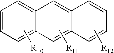
In the star-shaped oligothiophene-arylene derivative of Formula 1 according to the present invention, non-limiting representative examples of compounds corresponding to Ar2 include compounds represented by Formula 4 below:
Figure US08058457-20111115-C00006
wherein
R14 to R21 are independently hydrogen, hydroxyl, amine, C1-20 linear, branched or cyclic alkyl, alkoxy, C1-20 alkoxyalkyl, alkylamine, ester or amide.
Specific examples of the compounds of Formula 4 include, but are not limited to, C5-30 aromatic compounds, for example, benzenes, naphthalenes, anthracenes, and fluorenes.
The star-shaped oligothiophene-arylene derivative of the embodiments of the present invention can be synthesized by chemical or electrochemical oxidation and condensation using an organometallic compound of a transition metal, such as nickel or palladium, which are representative polymerization processes of heteroaromatic compounds.
That is, the star-shaped oligothiophene-arylene derivative of the embodiments of the present invention is synthesized by polymerizing compounds of Formulae 5 to 8 below:
Ar
Figure US08058457-20111115-Parenopenst
X1)m  Formula 5
wherein Ar is as defined in Formula 1, X1 is Br, Cl, or I, and m is an integer between 3 and 8;
Figure US08058457-20111115-C00007
wherein Ar1 is as defined in Formula 1, X2 is a trialkyltin group, a dioxaborane group, or boronic acid, and n1 is an integer between 0 and 6;
Figure US08058457-20111115-C00008
wherein R is as defined in Formula 1, X3 is a trialkyltin group, a dioxaborane group, or boronic acid, and n2 is an integer between 2 and 8; and
Figure US08058457-20111115-C00009
wherein Ar2 is as defined in Formula 1, X4 is a trialkyltin group, a dioxaborane group, or boronic acid, and n3 is an integer between 0 and 6,
at 70-130° C. in the presence of at least one catalyst represented by Formulae 9 to 11 below:
PdL4  Formula 9
wherein L is a ligand selected from the group consisting of triphenylphosphine (PPh3), triphenylarsine (AsPh3), triphenylphosphite (P(OPh)3), diphenylphosphinoferrocene (dppf), diphenylphosphino butane (dppb), acetate (OAc), and dibenzylideneacetone (dba);
PdL2X2  Formula 10
wherein L is as defined in Formula 9, and X is I, Br or Cl; and
PdL2  Formula 11
wherein L is as defined in Formula 9.
Specifically, the star-shaped oligothiophene-arylene derivative of the embodiments of the present invention is synthesized through the reaction paths depicted by the following Reaction Scheme 1:
Figure US08058457-20111115-C00010
Figure US08058457-20111115-C00011
The star-shaped oligothiophene-arylene derivative is synthesized by the Suzuki coupling reaction. One example of a star-shaped oligothiophene-arylene derivative that can be synthesized by the Suzuki coupling reaction is the compound represented by Formula 12 below:
Figure US08058457-20111115-C00012
Halide-substituted arylene derivatives (e.g., the compound of Formula 5) and boron-substituted compounds (e.g., the compounds of Formulae 6 to 8) are used to synthesize the star-shaped oligothiophene-arylene derivative of Formula 12. Compounds used to prepare the oligothiophene-arylene derivative of Formula 12, an embodiment of the present invention, are those represented by Formulae 13 and 14 below:
Figure US08058457-20111115-C00013
Figure US08058457-20111115-C00014
The star-shaped oligothiophene-arylene derivative of the embodiments of the present invention can be used as a novel organic semiconductor material for an active layer of an OTFT. General organic thin film transistors have structures of a substrate/a gate electrode/a gate insulating layer/an organic active layer/source-drain electrodes, a substrate/a gate electrode/a gate insulating layer/source-drain electrodes/an organic active layer, and the like, but are not limited to these structures.
At this time, the star-shaped oligothiophene-arylene derivative of the embodiments of the present invention can be formed into a thin film by, for example, screen printing, printing, spin coating, dipping, or ink spraying.
The gate insulating layer constituting the OTFT can be made of common high-dielectric constant insulators. Specific examples of suitable insulators include, but are not limited to, ferroelectric insulators, e.g., Ba0.33Sr0.66TiO3 (BST), Al2O3, Ta2O5, La2O5, Y2O3, and TiO2; inorganic insulators, e.g., PbZr0.33Ti0.66O3 (PZT), Bi4Ti3O12, BaMgF4, SrBi2(TaNb)2O9, Ba(ZrTi)O3 (BZT), BaTiO3, SrTiO3, Bi4Ti3O12, SiO2, SiNx, and AlON; and organic insulators, e.g., polyirpides, benzocyclobutenes (BCBs), parylenes, polyacrylates, polyvinylalcohols, polyvinylphenols, and the like.
The substrate can be made of, but is not limited to, glass, polyethylenenaphthalate (PEN), polyethyleneterephthalate (PET), polycarbonate, polyvinylalcohol, polyacrylate, polyimide, polynorbornene, polyethersulfone (PES), and the like.
The gate electrode and source-drain electrodes can be made of common metals. Specific examples of such metals include, but are not limited to, gold (Au), silver (Ag), aluminum (Al), nickel (Ni), indium tin oxide (ITO), and molybdenum/tungsten (Mo/W).
Embodiments of the present invention will now be described in more detail with reference to the following examples. However, these examples are given for the purpose of illustration and are not to be construed as limiting the scope of the invention.
Preparative Example 1 Preparation of Oligothiophene Borolanes 1 and 2
Figure US08058457-20111115-C00015
n-BuLi in tetrahydrofuran (THF) was added to 3-hexyl thiophene at −20° C., and then N,N,N′,N′-tetramethylethylenediamine (TMEDA) was added thereto. The mixture was heated to 70° C. for 3 hours. Subsequently, dioxaborolane was added to the mixture at −78° C. and was slowly allowed to warm to room temperature to obtain the oligothiophene borolane 1.
The oligothiophene borolane 1 and 2-bromothiophene were added to a mixture of toluene and water, and then tetrakis(triphenylphosphine)palladium (0) (Pd(PPh3)4, Aldrich) as a catalyst and potassium carbonate were added thereto. The reaction mixture was allowed to react at 110° C. for 8 hours to obtain the compound 2a.
n-BuLi in tetrahydrofuran was added to the compound 2a at −20° C., and then N,N,N′,N′-tetramethylethylenediamine (TMEDA) was added thereto. The mixture was heated to 70° C. for 3 hours. Subsequently, dioxaborolane was added to the mixture at −78° C. and was slowly allowed to warm to room temperature to afford the oligothiophene borolane 2.
1H-NMR (300 MHz, CDCl3) δ (ppm) 0.89 (t, 3H, J=6.8 Hz), 6H), 1.21-1.35 (m, 18H), 1.59-1.66 (m, 2H), 2.58 (t, 2H, J=7.8 Hz), 6.68 (s, 1H), 7.00 (s, 1H), 7.20 (d, 1H, J=3.5 Hz), 7.47 (d, 1H, J=3.5 Hz)
Preparative Example 2 Preparation of Oligothiophene Borolanes 3 and 4
Figure US08058457-20111115-C00016
Thiophen-2-yl-magnesium bromide was added to a mixture of hexanal and THF to obtain the compound 3a. Zinc iodide, sodium cyanoborohydride and 1,2-dichloroethane were added to the compound 3a, and then the mixture was heated to 85° C. for 3 hours to obtain the compound 3b. Lithium diisopropylamide (LDA) in THF was added to the compound 3b at −78° C., and then dioxaborolane was added thereto to obtain the thiophene borolane 3. Thereafter, the thiophene borolane 3 and 2-bromobithiophene were reacted under the same conditions as in the preparation of the compound 2a indicated in Preparative Example 1 to obtain the compound 4a. Lithium diisopropylamide (LDA) in THF was added to the compound 4a at −78° C., and then dioxaborolane was added thereto to afford the oligothiophene borolane 4.
1H-NMR (300 MHz, CDCl3) δ (ppm) 0.89 (t, 3H, J=6.8 Hz), 1.25-1.43 (m, 18H), 1.60-1.75 (m, 2H), 2.78 (t, 2H, J=7.5 Hz), 6.65 (d, 1H, J=3.5 Hz), 7.04 (d, 1H, J=3.5 Hz), 7.15 (d, 1H, J=3.5 Hz), 7.49 (d, 1H, J=3.5 Hz)
Preparative Example 3 Preparation of Oligothiophene-Arylene Derivative 1
Figure US08058457-20111115-C00017
Figure US08058457-20111115-C00018
2,4,6,8-Tetrachloro-pyrimido[5,4-d]pyrimidine (TCl) and the oligothiophene borolane 2 were subjected to condensation by the Suzuki coupling reaction to obtain the compound 1a. To the compound 1a was added N-bromosuccinimide (NBS) in chloroform to obtain the dibromide 1b. The dibromide 1b and the oligothiophene borolane 4 were mixed with toluene and water, and then Pd(PPh3)4 as a catalyst and potassium carbonate in a solvent were added thereto. The resulting mixture was heated to 110° C. for 8 hours and washed with an aqueous ammonium chloride solution. The obtained organic layer was distilled under reduced pressure and purified by silica gel column chromatography, affording the derivative 1.
1H-NMR (300 MHz, CDCl3) δ (ppm) 0.85-0.94 (m, 24H), 1.29-1.42 (m, 48H), 1.56-1.63 (m, 8H), 1.63-1.76 (m, 8H), 2.53-2.65 (m, 8H), 2.73-2.81 (m, 8H), 6.50-6.60 (m, 4H), 6.81-6.90 (m, 20H), 7.52 (s, 2H), 8.28 (s, 2H)
Fabrication of OTFTs Example 1 Fabrication of Organic Thin Film Transistor Using Oligothiophene-Arylene Derivative 1
First, molybdenum/tungsten (Mo/W) were deposited on a glass substrate that had been previously washed by a sputtering process to form a gate electrode having a thickness of 1,000 Å. Thereafter, a polyacrylate-based polymer was deposited on the gate electrode by a spin-coating process to form a gate insulating film, and was then dried at 150° C. for one hour. Gold (Au) as a material for source-drain electrodes was deposited on the gate insulating layer to a thickness of 500 Å by a sputtering process. Separately, the oligothiophene-arylene derivative 1 prepared in Preparative Example 3 was dissolved in toluene to obtain a 2 wt % solution. The solution was applied to the resulting structure at 1,000 rpm to a thickness of 800 Å, and baked at 100° C. for one hour to fabricate an OTFT as schematically illustrated in FIG. 1.
Comparative Example 1
An organic thin film transistor was fabricated in the same manner as in Example 1, except that polyhexylthiophene HT-P3HT (Aldrich) was used.
Evaluation of Electrical Properties of OTFTs
The charge carrier mobility of the devices fabricated in Example 1 and Comparative Example 1 was measured. The current transfer characteristics of the devices were evaluated using a KEITHLEY semiconductor characterization system (4200-SCS), and curves were plotted. The obtained results are shown in Table 1. The charge carrier mobility was calculated using the curve from the following current equations in the saturation region.
The charge carrier mobility was calculated from the slope of a graph representing the relationship between (ISD)1/2 and VG from the following current equations in the saturation region:
I SD = WC 0 2 L μ ( V G - V T ) 2 I SD = μ C 0 W 2 L ( V G - V T ) slope = μ C 0 W 2 L μ FET = ( slope ) 2 2 L C 0 W
In the above equations, ISD: source-drain current, μ and μFET: charge carrier mobility, Co: capacitance of the oxide film, W: channel width, L: channel length; VG: gate voltage, and VT: threshold voltage.
Off-state leakage current (Ioff) is a current flowing in the off-state, and was determined from the minimum current in the off-state.
TABLE 1
Charge carrier mobility Off-state leakage
Organic active layer (cm2/Vs) current (A)
Example 1 0.00005 1 × 10⁻¹²
Comparative Example 1 0.01 1 × 10⁻⁸ 
(HT-P3HT)
As can be seen from the data shown in Table 1, the oligothiophene-arylene derivatives of the present invention showed a considerably low off-state leakage current of 1×10⁻¹² A and a high charge carrier mobility of 0.00005.
As apparent from the foregoing, the star-shaped oligothiophene-arylene derivative of the present invention is a low-molecular weight organic semiconductor material with a novel structure. In addition, since the oligothiophene-arylene derivative can be spin-coated at room temperature, is stable, and exhibits low off-state leakage current, it can be used as a material for an active layer of an OTFT.
Although the preferred embodiments of the present invention have been disclosed for illustrative purposes, those skilled in the art will appreciate that various modifications, additions and substitutions are possible, without departing from the scope and spirit of the invention as disclosed in the accompanying claims.

Claims (5)

1. An organic thin film transistor comprising a substrate, a gate electrode, a gate insulating layer, an organic active layer and source-drain electrodes wherein the organic active layer is made of a star-shaped oligothiophene-arylene compound including an oligothiophene having p-type semiconductor characteristics bonded to an arylene having n-type semiconductor characteristics, the oligothiophene positioned in a central moiety of the molecule, represented by Formula 1 below, to form a star shape with the arylene:
Figure US08058457-20111115-C00019
wherein Ar is selected from groups represented by Formula 2 below:
Figure US08058457-20111115-C00020
wherein R1, R2, R3, and R4 are independently hydrogen, hydroxyl, amine group, C1-20 linear, branched or cyclic alkyl, alkoxy, C1-20 alkoxyalkyl, alkylamine group, ester group or amide group,
wherein Ar1 is selected from groups represented by Formula 3 below:
Figure US08058457-20111115-C00021
wherein R5, R6, R7, R8, R9, R10, R11, R12, R13 are independently hydrogen, a hydroxyl group, an amine group, a C1-20 linear, branched or cyclic alkyl group, an alkoxy group, a C1-20 alkoxyalkyl group, an alkylamine group, an ester group or an amide group,
wherein Ar2 is selected from groups represented by Formula 4 below:
Figure US08058457-20111115-C00022
wherein R14, R15, R16, R17, R18, R19, R20, R21, are independently hydrogen, a hydroxyl group, an amine group, a C1-20 linear, branched or cyclic alkyl group, an alkoxy group, a C1-20 alkoxyalkyl group, an alkylamine group, an ester group or an amide group,
R is hydrogen, a hydroxyl group, an amine group, a C1-20 linear, branched or cyclic alkyl group, an alkoxy group, a C1-20 alkoxyalkyl group, an alkylamine group, an ester group or an amide group,
n is an integer between 3 and 8,
n1 and n3 are each independently an integer between 0 and 6, and
n2 is an integer between 2 and 8.
2. The organic thin film transistor according to claim 1, wherein the organic active layer is formed into a thin film by screen printing, printing, spin coating, dipping, or ink spraying.
3. The organic thin film transistor according to claim 1, wherein the gate insulating layer is made of a ferroelectric insulator selected from the group consisting of Ba0.33Sr0.66TiO3, Al2O3, Ta2O5, La2O5, Y2O3, and TiO2; an inorganic insulator selected from the group consisting of PbZr0.33Ti0.66O3, Bi4Ti3O12, BaMgF4, SrBi2(TaNb)2O9, Ba(ZrTi)O3, BaTiO3, SrTiO3, Bi4Ti3O12, SiO2, SiNX, and AlON; or an organic insulator selected from the group consisting of polyimides, benzocyclobutenes, parylenes, polyacrylates, polyvinylalcohols, and polyvinyiphenols.
4. The organic thin film transistor according to claim 1, wherein the substrate is made of a material selected from the group consisting of glass, polyethylenenaphthalate, polyethyleneterephthalate, polycarbonate, polyvinylalcohol, polyacrylate, polyimide, polynorbornene, and polyethersulfone.
5. The organic thin film transistor according to claim 1, wherein the gate electrode and source-drain electrodes are independently made of a material selected from the group consisting of gold, silver, aluminum, nickel, indium tin oxide, and molybdenum/tungsten.
US12/656,831 2004-11-29 2010-02-17 Star-shaped oligothiophene-arylene derivatives and organic thin film transistors using the same Expired - Fee Related US8058457B2 (en)

Priority Applications (1)

Application Number Priority Date Filing Date Title
US12/656,831 US8058457B2 (en) 2004-11-29 2010-02-17 Star-shaped oligothiophene-arylene derivatives and organic thin film transistors using the same

Applications Claiming Priority (4)

Application Number Priority Date Filing Date Title
KR1020040098674A KR101151082B1 (en) 2004-11-29 2004-11-29 Star-shaped (Oligothiophene-Arylene) derivatives and Organic Thin Film Transistor using the same
KR04-98674 2004-11-29
US11/116,326 US7692029B2 (en) 2004-11-29 2005-04-28 Star-shaped oligothiophene-arylene derivatives and organic thin film transistors using the same
US12/656,831 US8058457B2 (en) 2004-11-29 2010-02-17 Star-shaped oligothiophene-arylene derivatives and organic thin film transistors using the same

Related Parent Applications (1)

Application Number Title Priority Date Filing Date
US11/116,326 Division US7692029B2 (en) 2004-11-29 2005-04-28 Star-shaped oligothiophene-arylene derivatives and organic thin film transistors using the same

Publications (2)

Publication Number Publication Date
US20100230663A1 US20100230663A1 (en) 2010-09-16
US8058457B2 true US8058457B2 (en) 2011-11-15

Family

ID=36566525

Family Applications (2)

Application Number Title Priority Date Filing Date
US11/116,326 Active 2028-02-11 US7692029B2 (en) 2004-11-29 2005-04-28 Star-shaped oligothiophene-arylene derivatives and organic thin film transistors using the same
US12/656,831 Expired - Fee Related US8058457B2 (en) 2004-11-29 2010-02-17 Star-shaped oligothiophene-arylene derivatives and organic thin film transistors using the same

Family Applications Before (1)

Application Number Title Priority Date Filing Date
US11/116,326 Active 2028-02-11 US7692029B2 (en) 2004-11-29 2005-04-28 Star-shaped oligothiophene-arylene derivatives and organic thin film transistors using the same

Country Status (4)

Country Link
US (2) US7692029B2 (en)
JP (1) JP4939044B2 (en)
KR (1) KR101151082B1 (en)
CN (1) CN1978439A (en)

Cited By (2)

* Cited by examiner, † Cited by third party
Publication number Priority date Publication date Assignee Title
US20100234595A1 (en) * 2009-03-16 2010-09-16 Fuji Xerox Co., Ltd. Nitrogen-containing heterocyclic compound
US20120015399A1 (en) * 2009-02-06 2012-01-19 National University Corporation Hokkaido University Fluorescent solvatochromic pigment

Families Citing this family (13)

* Cited by examiner, † Cited by third party
Publication number Priority date Publication date Assignee Title
KR20060081441A (en) * 2005-01-07 2006-07-13 삼성전자주식회사 Novel thiophene-thiazole derivatives and organic thin film transistors using the same
KR101139038B1 (en) * 2005-06-28 2012-05-02 삼성전자주식회사 Pyrimidopyrimidine Derivatives and Organic Thin Film Transistor Using The Same
CN100544052C (en) * 2006-06-21 2009-09-23 中国科学院化学研究所 Field-effect transistor of organic semiconductor material and preparation method thereof
JP5117763B2 (en) * 2007-05-21 2013-01-16 山本化成株式会社 Organic transistor
CN102549791B (en) 2009-08-28 2015-01-07 新加坡科技研究局 Ambipolar polymeric semiconductor materials and organic electronic devices
KR101867784B1 (en) 2009-08-28 2018-06-15 에이전시 포 사이언스, 테크놀로지 앤드 리서치 Polymeric semiconductors, devices, and related methods
JP5778162B2 (en) * 2009-10-22 2015-09-16 エージェンシー フォー サイエンス,テクノロジー アンド リサーチ N-type materials and organic electronic devices
WO2011130922A1 (en) * 2010-04-23 2011-10-27 海洋王照明科技股份有限公司 Copolymer comprising anthracene and benzoselenadiazole, preparing method and uses thereof
EP2576645B1 (en) * 2010-06-04 2015-03-18 Tongji University Copolymer of pyrene and pyrrole and method of producing the copolymer
US9336921B2 (en) 2013-12-17 2016-05-10 Dow Global Technologies Llc Electrically conducting composites, methods of manufacture thereof and articles comprising the same
US9330809B2 (en) 2013-12-17 2016-05-03 Dow Global Technologies Llc Electrically conducting composites, methods of manufacture thereof and articles comprising the same
KR101577900B1 (en) * 2014-06-24 2015-12-29 동국대학교 산학협력단 Thin-film transistor using sectional etching and preparing there of
CN108602826A (en) * 2016-02-04 2018-09-28 默克专利有限公司 [1,5]Naphthyridine compounds and polymers as semiconductors

Citations (5)

* Cited by examiner, † Cited by third party
Publication number Priority date Publication date Assignee Title
US6107117A (en) 1996-12-20 2000-08-22 Lucent Technologies Inc. Method of making an organic thin film transistor
WO2000079617A1 (en) 1999-06-21 2000-12-28 Cambridge University Technical Services Limited Aligned polymers for an organic tft
WO2004013122A2 (en) 2002-07-26 2004-02-12 Infineon Technologies Ag Octupolar molecules used as organic semi-conductors
US7368510B2 (en) * 2004-07-08 2008-05-06 Samsung Electronics Co., Ltd. Organic semiconductor copolymers containing oligothiophene and n-type heteroaromatic units
US7541424B2 (en) * 2004-10-19 2009-06-02 Samsung Electronics Co., Ltd. Oligothiophene-arylene derivatives and organic thin film transistors using the same

Patent Citations (5)

* Cited by examiner, † Cited by third party
Publication number Priority date Publication date Assignee Title
US6107117A (en) 1996-12-20 2000-08-22 Lucent Technologies Inc. Method of making an organic thin film transistor
WO2000079617A1 (en) 1999-06-21 2000-12-28 Cambridge University Technical Services Limited Aligned polymers for an organic tft
WO2004013122A2 (en) 2002-07-26 2004-02-12 Infineon Technologies Ag Octupolar molecules used as organic semi-conductors
US7368510B2 (en) * 2004-07-08 2008-05-06 Samsung Electronics Co., Ltd. Organic semiconductor copolymers containing oligothiophene and n-type heteroaromatic units
US7541424B2 (en) * 2004-10-19 2009-06-02 Samsung Electronics Co., Ltd. Oligothiophene-arylene derivatives and organic thin film transistors using the same

Non-Patent Citations (20)

* Cited by examiner, † Cited by third party
Title
Audebert, et al.; First example-tetrazine; Elsevier Science B.V.; 2004; Chem Abstract 140:339765.
Bang Lin Lee, et al. "Synthesis of New Alternating CT-Type Copolymers of Thiophene and Pyrido[3,4b]pyrazine Units: Their Optical and Electrochemical Properties in Comparison with Similar CT Copolymers of Thiophene with Pyridine and Quinoxaline", Macromolecules, vol. 32, pp. 1375-1382, 1999.
Cherioux et al., Chem. Commun., 2225-2226, 1998.
Cherioux, et al., "Synthesis and characterisation of an octupolar polymer and new molecular octupoles with off-resonant third order optical nonlinearities", Jul. 1999, pp. 2083-2084.
David J. Brennan et al., "Polyfluorenes as Organic Semiconductors for Polymeric Field Effect Transistors", Mat. Res. Soc. Symp. Proc., 2003 Materials Research Societs, pp. L6.1.1-L.6.1.6, vol. 771.
David J. Brennan, et al., "Polyfluorenes as Organic Semiconductors for Polymeric Field Effect Transistors", Mat. Res. Soc. Symo. Proc. vol. 771, 2003 Materials Research Society, pp. L6.1.1-L6.1.6.
Divisia-Blohorn, et al.; Conjugated-interactions; American Chemical Society; 2003; Chem Abstract 139: 59502.
Francis Garnier et al., "Molecular Engineering of Organic Semiconductors Design of Self-Assembly Properties in Conjugated Thiophene Oligomers", J. Am. Chem. Soc., 1993, pp. 8718-8721, vol. 115.
Francis Garnier, et al., "Molecular Engineering of Organic Semiconductors: Design of Self-Assembly Properties in Conjugates Thiophene Oligomers" J. Am. Chem. Soc. 1993 vol. 115, pp. 8716-8721.
H. Sirringhaus et al., "High-Resolution Inkjet Printing of All-Polymer Transistor Circuits", Science, Dec. 15, 2000, pp. 2123-2126, vol. 290.
H. Sirringhaus, et al., "High-Resolution Inkjet Printing of All-Polymer Transistor Circuits," Science, vol. 290, Dec. 15, 2000, pp. 2123-2126.
Halik, et al.; Octupolar molecules-semiconductors; Infineon Technologies AG, Germany ; Feb. 2004; Chem Abstract 140: 173273.
Office Action dated Jun. 21, 2011 for corresponding Japanese Patent Application No. 2005-343010.
Sandrine Martin et al., "Source/Drain Contacts in Organic Polymer Thin Film Transistors", Mat. Res. Soc. Symp. Proc., 2003 Materials Research Society, pp. L6.2.1-L6.2.5, vol. 771.
Sandrine Martin, et al., "Source/drain contacts in organic polymer thin film transistors" Mat. Res. Soc. Symo. Proc. vol. 771, 2003 Materials Research Society, pp. L6.2.1-L6.2.6.
Sauvage, et al.; Comjugated polyrotaxanes; Royal Society of Chemistry; 2002; Chem Abstract 138: 39668.
Sergei A. Ponomarenko et al., "Star-Shaped Oligothiophenes for Solution-Processible Organic Field-Effect Transistors", Advanced Functional Materials, vol. 13, pp. 591-596, 2003.
Suzuki, et al.; Organic luminescence device; Canon Kabushiki Kaisha, Japan; 2003; Chem Abstract 138: 245328.
Tommie W. Kelley et al., "High Performance Organic Thin Film Transistors", Mat. Res. Soc. Symp. Proc., 2003 Materials Research Society, pp. L6.5.1-L6.5.11, vol. 771.
Tommie W. Kelley, et al., "High Performance Organic Thin Film Transistors", Mat. Res. Soc. Symo. Proc. vol. 771, 2003 Materials Research Society, pp. L6.5.1-L6.5.11.

Cited By (4)

* Cited by examiner, † Cited by third party
Publication number Priority date Publication date Assignee Title
US20120015399A1 (en) * 2009-02-06 2012-01-19 National University Corporation Hokkaido University Fluorescent solvatochromic pigment
US20100234595A1 (en) * 2009-03-16 2010-09-16 Fuji Xerox Co., Ltd. Nitrogen-containing heterocyclic compound
US8222409B2 (en) * 2009-03-16 2012-07-17 Fuji Xerox Co., Ltd. Nitrogen-containing heterocyclic compound
US8420814B2 (en) 2009-03-16 2013-04-16 Fuji Xerox Co., Ltd. Nitrogen-containing heterocyclic compound

Also Published As

Publication number Publication date
CN1978439A (en) 2007-06-13
US20060113527A1 (en) 2006-06-01
JP4939044B2 (en) 2012-05-23
US20100230663A1 (en) 2010-09-16
KR20060059551A (en) 2006-06-02
US7692029B2 (en) 2010-04-06
KR101151082B1 (en) 2012-06-01
JP2006151981A (en) 2006-06-15

Similar Documents

Publication Publication Date Title
US8058457B2 (en) Star-shaped oligothiophene-arylene derivatives and organic thin film transistors using the same
US7923529B2 (en) Oligothiophene-arylene derivatives and organic thin film transistors using the same
US8008426B2 (en) Organic semiconductor polymer having liquid crystal properties, organic active layer, organic thin film transistor, and electronic device including the same, and methods of fabricating the same
US7719000B2 (en) Organic semiconductor materials using stacking-inducing compounds, compositions comprising such materials, organic semiconductor thin films formed using such compositions, and organic electronic devices incorporating such thin films
US7030409B2 (en) Organic semiconductor polymer for organic thin film transistor containing quinoxaline ring in the backbone chain
EP1434285A2 (en) Organic semiconductor polymer and organic thin film transistor
US20120077949A1 (en) Organic semiconductor copolymers containing oligothiophene and n-type heteroaromatic units
KR101450137B1 (en) Copolymer for organic semiconductor and organic thin film transistor and organic electronic device using same
KR20130057951A (en) Organic semiconductor compound, organic thin film including the organic semiconductor compound electronic device including the organic thin film and method of manufacturing the organic thin film
US7632947B2 (en) Pyrimidopyrimidine derivatives, organic thin film transistors using pyrimidopyrimidine derivatives and method for fabricating the same
KR101072477B1 (en) Organic semiconductor compounds substituted alkylthiophen group in side-chain of polymer and organic thin film transistor utilizing same
JP4891618B2 (en) Thiophene-thiazole derivatives and organic thin film transistors using them
US9705094B2 (en) Organic semiconductor compound, organic thin film including same, and electronic device including the organic thin film
KR101254100B1 (en) Novel organic semiconductor and Organic thin film transistor using the same
US9790236B2 (en) Organic semiconductor compound, and transistor and electronic device including the same
KR20060108173A (en) Novel polythiophene derivatives and organic thin film transistors using the same

Legal Events

Date Code Title Description
ZAAA Notice of allowance and fees due

Free format text: ORIGINAL CODE: NOA

ZAAB Notice of allowance mailed

Free format text: ORIGINAL CODE: MN/=.

STCF Information on status: patent grant

Free format text: PATENTED CASE

FEPP Fee payment procedure

Free format text: PAYOR NUMBER ASSIGNED (ORIGINAL EVENT CODE: ASPN); ENTITY STATUS OF PATENT OWNER: LARGE ENTITY

FPAY Fee payment

Year of fee payment: 4

MAFP Maintenance fee payment

Free format text: PAYMENT OF MAINTENANCE FEE, 8TH YEAR, LARGE ENTITY (ORIGINAL EVENT CODE: M1552); ENTITY STATUS OF PATENT OWNER: LARGE ENTITY

Year of fee payment: 8

FEPP Fee payment procedure

Free format text: MAINTENANCE FEE REMINDER MAILED (ORIGINAL EVENT CODE: REM.); ENTITY STATUS OF PATENT OWNER: LARGE ENTITY

LAPS Lapse for failure to pay maintenance fees

Free format text: PATENT EXPIRED FOR FAILURE TO PAY MAINTENANCE FEES (ORIGINAL EVENT CODE: EXP.); ENTITY STATUS OF PATENT OWNER: LARGE ENTITY

STCH Information on status: patent discontinuation

Free format text: PATENT EXPIRED DUE TO NONPAYMENT OF MAINTENANCE FEES UNDER 37 CFR 1.362

FP Lapsed due to failure to pay maintenance fee

Effective date: 20231115