US8054358B2 - Solid state image pickup device - Google Patents
Solid state image pickup device Download PDFInfo
- Publication number
- US8054358B2 US8054358B2 US12/275,681 US27568108A US8054358B2 US 8054358 B2 US8054358 B2 US 8054358B2 US 27568108 A US27568108 A US 27568108A US 8054358 B2 US8054358 B2 US 8054358B2
- Authority
- US
- United States
- Prior art keywords
- terminal
- transistor
- output
- terminal connected
- source
- Prior art date
- Legal status (The legal status is an assumption and is not a legal conclusion. Google has not performed a legal analysis and makes no representation as to the accuracy of the status listed.)
- Active, expires
Links
- 239000007787 solid Substances 0.000 title 1
- 230000003321 amplification Effects 0.000 claims abstract description 67
- 238000003199 nucleic acid amplification method Methods 0.000 claims abstract description 67
- 238000009792 diffusion process Methods 0.000 claims abstract description 44
- 238000012546 transfer Methods 0.000 claims abstract description 25
- 239000000654 additive Substances 0.000 claims description 23
- 230000000996 additive effect Effects 0.000 claims description 23
- 238000010276 construction Methods 0.000 claims description 14
- 239000000758 substrate Substances 0.000 claims description 12
- 230000008878 coupling Effects 0.000 claims description 8
- 238000010168 coupling process Methods 0.000 claims description 8
- 238000005859 coupling reaction Methods 0.000 claims description 8
- 239000004065 semiconductor Substances 0.000 claims description 6
- 239000011159 matrix material Substances 0.000 claims description 4
- 238000010586 diagram Methods 0.000 description 10
- 238000000079 presaturation Methods 0.000 description 9
- 239000006185 dispersion Substances 0.000 description 6
- 238000004088 simulation Methods 0.000 description 5
- 238000012937 correction Methods 0.000 description 4
- 230000000694 effects Effects 0.000 description 4
- 230000035945 sensitivity Effects 0.000 description 4
- 230000006870 function Effects 0.000 description 3
- 238000004519 manufacturing process Methods 0.000 description 3
- 238000012360 testing method Methods 0.000 description 3
- 238000011282 treatment Methods 0.000 description 3
- 229920006395 saturated elastomer Polymers 0.000 description 2
- 238000000342 Monte Carlo simulation Methods 0.000 description 1
- 230000008901 benefit Effects 0.000 description 1
- 230000000295 complement effect Effects 0.000 description 1
- 230000000593 degrading effect Effects 0.000 description 1
- 230000001419 dependent effect Effects 0.000 description 1
- 238000013461 design Methods 0.000 description 1
- 230000006866 deterioration Effects 0.000 description 1
- 230000006872 improvement Effects 0.000 description 1
- 239000012535 impurity Substances 0.000 description 1
- 230000007246 mechanism Effects 0.000 description 1
- 239000002184 metal Substances 0.000 description 1
- 229910044991 metal oxide Inorganic materials 0.000 description 1
- 150000004706 metal oxides Chemical class 0.000 description 1
- 238000000034 method Methods 0.000 description 1
- 238000012986 modification Methods 0.000 description 1
- 230000004048 modification Effects 0.000 description 1
- 238000012545 processing Methods 0.000 description 1
- 238000000926 separation method Methods 0.000 description 1
- 229910052710 silicon Inorganic materials 0.000 description 1
- 239000010703 silicon Substances 0.000 description 1
Images


Classifications
-
- H—ELECTRICITY
- H04—ELECTRIC COMMUNICATION TECHNIQUE
- H04N—PICTORIAL COMMUNICATION, e.g. TELEVISION
- H04N25/00—Circuitry of solid-state image sensors [SSIS]; Control thereof
- H04N25/50—Control of the SSIS exposure
- H04N25/57—Control of the dynamic range
-
- H—ELECTRICITY
- H04—ELECTRIC COMMUNICATION TECHNIQUE
- H04N—PICTORIAL COMMUNICATION, e.g. TELEVISION
- H04N25/00—Circuitry of solid-state image sensors [SSIS]; Control thereof
- H04N25/60—Noise processing, e.g. detecting, correcting, reducing or removing noise
- H04N25/67—Noise processing, e.g. detecting, correcting, reducing or removing noise applied to fixed-pattern noise, e.g. non-uniformity of response
- H04N25/671—Noise processing, e.g. detecting, correcting, reducing or removing noise applied to fixed-pattern noise, e.g. non-uniformity of response for non-uniformity detection or correction
- H04N25/672—Noise processing, e.g. detecting, correcting, reducing or removing noise applied to fixed-pattern noise, e.g. non-uniformity of response for non-uniformity detection or correction between adjacent sensors or output registers for reading a single image
-
- H—ELECTRICITY
- H04—ELECTRIC COMMUNICATION TECHNIQUE
- H04N—PICTORIAL COMMUNICATION, e.g. TELEVISION
- H04N25/00—Circuitry of solid-state image sensors [SSIS]; Control thereof
- H04N25/70—SSIS architectures; Circuits associated therewith
- H04N25/76—Addressed sensors, e.g. MOS or CMOS sensors
- H04N25/77—Pixel circuitry, e.g. memories, A/D converters, pixel amplifiers, shared circuits or shared components
-
- H—ELECTRICITY
- H10—SEMICONDUCTOR DEVICES; ELECTRIC SOLID-STATE DEVICES NOT OTHERWISE PROVIDED FOR
- H10F—INORGANIC SEMICONDUCTOR DEVICES SENSITIVE TO INFRARED RADIATION, LIGHT, ELECTROMAGNETIC RADIATION OF SHORTER WAVELENGTH OR CORPUSCULAR RADIATION
- H10F39/00—Integrated devices, or assemblies of multiple devices, comprising at least one element covered by group H10F30/00, e.g. radiation detectors comprising photodiode arrays
- H10F39/10—Integrated devices
- H10F39/12—Image sensors
- H10F39/18—Complementary metal-oxide-semiconductor [CMOS] image sensors; Photodiode array image sensors
Definitions
- the technical field of this invention is a solid-state image pickup device. Especially, the present invention pertains to a CMOS type or CCD type solid-state image pickup device.
- CMOS Complementary Metal Oxide Semiconductor
- CCD Charge Coupling Device
- CMOS image sensors or other solid-state image pickup devices A very important factor in such CMOS image sensors or other solid-state image pickup devices is whether the signal charge obtained at the photodiode of each pixel can be transferred to the output without any loss. This character determines the image quality. The linearity between the voltage corresponding to the signal charge and the output voltage from the pixel is thus an important factor.
- FIG. 11 is a circuit diagram illustrating a source follower circuit used for reading the charge accumulated in each pixel as a voltage.
- This source follower includes one NMOS transistor M 1 .
- the gate electrode of transistor M 1 is connected to a floating diffusion region that stores the charge of each pixel.
- the voltage V in corresponds to the stored charge.
- a predetermined voltage VR is applied via a selecting transistor not shown to one end of the source/drain path.
- the other end of the source/drain path connects to output line V out .
- the gate-source voltage V gs equals threshold voltage V th ⁇ V out ⁇ .
- the output voltage V out becomes V in ⁇ V th ⁇ V out ⁇ .
- V th is influenced by the bias of the substrate as shown in equation (1).
- V th V th0 + ⁇ ⁇ ( ⁇ 2 ⁇ ⁇ ⁇ F + V out ⁇ - ⁇ 2 ⁇ ⁇ ⁇ F ⁇ ) ⁇ ⁇
- ⁇ Si is the dielectric constant of silicon
- N sub is impurity concentration in the substrate
- C ox is the capacitance of the gate oxide film
- n i is the true carrier density
- k is the Boltzmann constant
- T represents the absolute temperature.
- V th is a function of the output voltage and does not have a constant value. This leads to deterioration in the linearity between the voltage of the signal charge and output voltage of the pixel. As a result, the image quality of the solid-state image pickup device depends upon the performance of the source follower.
- the problem addressed by the present invention is improving the linearity of the source follower in a CMOS image sensor or other solid-state image pickup device to improve the image quality.
- This invention is a solid-state image pickup device including: plural pixels integrated in an array configuration on a semiconductor substrate, each pixel having a photodiode that receives light, generates and stores a photoelectric charge, a transfer transistor that transfers photoelectric charge from the photodiode, a floating diffusion that transfers the photoelectric charge via the transfer transistor and an amplification transistor having a gate electrode connected to the floating diffusion; a compensating circuit having an amplifier receiving the output of the amplification transistor as input and a compensating transistor having a gate electrode connected to the output of the amplifier with negative feedback of the output of the compensating transistor to the amplifier.
- the amplification transistor and the compensating transistor preferably have substantially the same ratio of gate width to gate length.
- the current source for the amplification transistor and the current source for the compensating transistor preferably have substantially the same current.
- the compensating circuit is preferably set for each column of the pixels integrated in an array configuration.
- the pixel preferably has a selecting transistor connected in series with the amplification transistor for selecting the pixel according to a selection driving line input.
- the pixel preferably also has an additive capacitance element connected to the photodiode via the floating diffusion storing the photoelectric charge transferred via the transfer transistor from the photodiode and a capacitive coupling transistor that couples or separates the floating diffusion and the additive capacitance element.
- the pixel preferably also has a reset transistor connected to the additive capacitance element or the floating diffusion for discharge of photoelectric charge in the additive capacitance element and/or the floating diffusion.
- the solid-state image pickup device includes: M ⁇ N image pickup elements set in a matrix configuration with M and N being integers greater than 2; N output circuits for receiving the outputs of the image pickup elements; each the image pickup element having a photodiode, a floating diffusion region, a transfer transistor for transferring electric charge from the photodiode to the floating diffusion region, a reset transistor for resetting the potential of the floating diffusion region, an amplification transistor having a control terminal connected to the floating diffusion region and outputting a voltage corresponding to the potential of the floating diffusion region, and a selecting transistor connected in series with the amplification transistor selecting the image pickup element; each the output circuit has an amplifier with and input receiving the output of the amplification transistor, and an output transistor having its control terminal connected to the output of the amplifier with its output fed to the other input of the amplifier; the structure of the amplification transistor of the image pickup element and the output transistor of the output circuit being the same; and the output of the amplifier is fed as the output of the image pickup element.
- the solid-state image pickup device includes: a pixel region with M ⁇ N pixels set in a matrix configuration where M and N are integers 2 or more; N amplifiers for receiving the outputs of the Mth row of pixels as one input and selectively receiving the outputs of the 1st through (M ⁇ 1)th rows of pixels as another input; each pixel having a photodiode, a floating diffusion region, a transfer transistor for transferring electric charge from the photodiode to the floating diffusion region, a reset transistor for resetting the potential of the floating diffusion region and an amplification transistor having its control terminal connected to the floating diffusion region for outputting a voltage corresponding to the potential of the floating diffusion region; the output of the amplifier being fed to the control terminal of an amplification transistor of the Mth row of pixels; and the N amplifiers are respectively set as a row corresponding to the Mth row of pixels.
- the solid-state image pickup device of the present invention has a compensating circuit set on the output side of an amplification transistor. This improves the linearity between the voltage corresponding to the signal charge and the output voltage from the pixel enabling improved image quality.
- FIG. 1 is a plan view illustrating the layout of the CMOS image sensor of a first embodiment of the present invention
- FIG. 2 is a circuit diagram equivalent to FIG. 1 illustrating a pixel of a CMOS image sensor
- FIG. 3 is a diagram illustrating the equivalent circuit of the amplification transistor (source follower transistor) and the compensating circuit of each pixel of FIG. 1 ;
- FIG. 4 is an circuit diagram illustrating the circuit of the overall CMOS image sensor in the first embodiment of this invention.
- FIG. 5 is a plan view illustrating the layout of the CMOS image sensor of a second embodiment of this invention.
- FIG. 6 is a circuit diagram used in simulation of an embodiment of this invention.
- FIG. 7( a ) shows the input-output curve in the first embodiment of this invention
- FIG. 7( b ) shows the linearity error in the first embodiment of this invention
- FIG. 8( a ) shows the input-output curve in the second embodiment of this invention
- FIG. 8( b ) shows the linearity error in the second embodiment of this invention
- FIG. 9( a ) shows the input-output curve in the third embodiment of this invention.
- FIG. 9( b ) shows the linearity error in the third embodiment of this invention.
- FIG. 10( a ) shows the input-output curve in the fourth embodiment of this invention.
- FIG. 10( b ) shows the linearity error in the fourth embodiment of this invention.
- FIG. 11 illustrates a circuit diagram of the prior art showing a source follower for reading the charge accumulated in each pixel of a solid-state image pickup device as a voltage.
- PX is a pixel; CC, CC 1 and CC 2 are compensating pixels; DC, DC 1 and DC 2 are dummy pixels; Tr 1 is a transfer transistor; Tr 2 is a capacitive coupling transistor; Tr 3 is a reset transistor; Tr 4 (M 1 ) is an amplification transistor; Tr 5 is a selecting transistor; AP is an amplifier; M 2 is a compensating transistor; VR is a power source voltage; ⁇ T , ⁇ S , ⁇ R , ⁇ X , ⁇ S1+N1 , ⁇ N1 , ⁇ S1′+S2′+N2 , ⁇ N2 and ⁇ XCLR are driving lines; SL is a selecting line; SR H is a column shift register; SR V is a row shift register; AM is an analog memory; C S is an additive capacitance element; FD is a floating diffusion; and PD is a photodiode.
- the solid-state image pickup device of a first embodiment is a CMOS image sensor with a wide dynamic range.
- FIG. 1 is a plan view illustrating the layout of the CMOS image sensor of this first embodiment.
- Plural image elements (pixels) PX each include a photodiode, a transfer transistor, a floating diffusion (floating diffusion region) and an amplification transistor disposed on a semiconductor substrate and integrated to form an array of M rows and N columns.
- a compensating circuit for each column of the pixels PX is integrated in the array configuration.
- the compensating circuit includes an amplifier receiving as input the output of the amplification transistor and a compensating transistor having its gate connected to the output of the amplifier.
- the compensating circuit has negative feedback where the output of the compensating transistor is fed back to the amplifier.
- the compensating transistor is included in a compensating pixel CC having the same construction as an image pixel PX.
- the amplifier is included with the pixel region on the outer side of the pixel region containing pixels PX and compensating pixels CC.
- the compensating transistor in the compensating pixel CC corresponds to the amplification transistor in
- Dummy pixels DC are disposed adjacent to compensating pixel CC.
- Dummy pixel DC has the same construction as pixel PX.
- Dummy pixels DC are used for measuring the black level.
- Compensating pixels CC and dummy pixels DC in dummy regions not shown in FIG. 1 have the same construction as pixels PX and are disposed as needed in the periphery of the array-configuration pixels PX. Dummy regions improve the processing stability in the manufacturing process.
- FIG. 2 is an equivalent circuit diagram illustrating one pixel PX of a CMOS image sensor in the solid-state image pickup device of this first embodiment.
- the pixel PX is a so-called 5-transistor type CMOS image sensor including: photodiode PD that receives light, generates and stores photoelectric charge; transfer transistor Tr 1 that transfers the photoelectric charge from the photodiode PD; floating diffusion FD that transfers the photoelectric charge through the transfer transistor Tr 1 ; additive capacitance element Cs; capacitive coupling transistor Tr 2 that couples or separates the capacitance of floating diffusion FD and additive capacitance element Cs; reset transistor Tr 3 connected to floating diffusion FD for discharge of the photoelectric charge in the floating diffusion FD; amplification transistor (also known as source follower transistor) Tr 4 with its gate electrode connected to floating diffusion FD to amplify and convert the photoelectric charge in floating diffusion FD to a voltage signal; and selecting transistor Tr 5 connected in series with the amplification transistor Tr 4 for selecting the pixel. All the five
- driving line ⁇ T is connected to the gate of transfer transistor Tr 1
- driving line ⁇ S is connected to the gate of capacitive coupling transistor Tr 2
- driving line ⁇ R is connected to the gate electrodes of reset transistor Tr 3 .
- Pixel selecting line ⁇ X (SL) is driven by a row shift register and is connected to the gate electrode of selecting transistor Tr 5 .
- a predetermined supply voltage VR supplies one of the terminal of the source/drain paths of reset transistor Tr 3 and selecting transistor Tr 5 .
- An output-side of the source/drain path of amplification transistor Tr 4 is connected to output line V out1 .
- Amplification transistor Tr 4 is controlled by selecting transistor Tr 5 via pixel selecting line ⁇ X (SL) controlled by a column shift register and outputs a voltage signal.
- FIG. 3 is an equivalent circuit diagram illustrating the amplification transistor (source follower transistor) Tr 4 (M 1 ) and the compensating circuit that forms pixel PX of this embodiment.
- the compensating circuit receives the output side amplification transistor Tr 4 (M 1 ).
- the compensating circuit includes amplifier AP.
- Amplifier AP has a non-inverting input receiving the output of amplification transistor Tr 4 .
- Compensating transistor M 2 is connected similarly to amplification transistor Tr 4 .
- Compensating transistor M 2 has a gate electrode connected to the output of amplifier AP.
- the output of compensating transistor M 2 supplies an inverting input of amplifier AP.
- Amplifier AP may also be an op-amp (operational amplifier).
- Prescribed supply voltage VR is supplied to one terminal of the source/drain path of amplification transistors Tr 4 (M 1 ) and of compensating transistor M 2 .
- Amplification transistor Tr 4 (M 1 ) and compensating transistor M 2 preferably have the same construction including substantially the same ratio of gate width to gate length.
- Current source I 1 connected to amplification transistor Tr 4 (M 1 ) and current source I 2 connected to compensating transistor M 2 have substantially the same current.
- pixel PX and compensating pixel CC have the same construction, and amplification transistor M 1 and compensating transistor M 2 have a corresponding relationship to each other.
- a circuit having a compensating circuit including compensating pixels CC for each column of pixels PX may have dummy pixels DC.
- Compensating pixels CC disposed near these dummy pixels DC have the same construction as previously described and are used as compensating transistors to compensate the transistors corresponding to the amplification transistors of the dummy pixels DC.
- Using a compensating circuit for each column of pixels PX integrated in an array results in reduced area needed for the compensating circuits as compared with the case of compensating circuit for each pixel.
- FIG. 3 shows gate-source voltage V gs1 with respect to source voltage V out1 of amplification transistor Tr 4 (M 1 ) is equal to threshold voltage V th1 which depends upon source voltage V out1 expressed as V th1 ⁇ V out ⁇ .
- Gate-source voltage V gs2 with respect to source voltage V out2 of compensating transistor M 2 is equal to threshold voltage V th2 which depends upon source voltage V out2 expressed as V th2 ⁇ V out2 ⁇ .
- input voltage V in to the gate of amplification transistor Tr 4 (M 1 ) which corresponds to the charge accumulated in the floating diffusion, source voltage V out1 of amplification transistor Tr 4 (M 1 ) is represented by equation (4).
- V out1 V in ⁇ V th1 ⁇ V out1 ⁇ (4)
- V out ⁇ ⁇ 2 A 1 + A ⁇ V out ⁇ ⁇ 1 + 1 1 + A ⁇ V th ⁇ ⁇ 2 ⁇ ⁇ V out ⁇ ⁇ 2 ⁇ ( 6 )
- V out2 of compensating transistor M 2 can be represented by equation (7).
- the approximations made for the first two lines result from the fact that when the amplification rate A of amplifier AP is sufficiently high V out2 approximates V out1 as noted in equation (7).
- the approximations made for the second and third lines result from matching amplification transistor Tr 4 (M 1 ) and compensating transistor M 2 and thus V th1 equals V th2 with these threshold voltages also includes a substrate bias effect.
- Equation (8) shows output V 1in of amplifier AP follows voltage V in applied to the gate of amplification transistor Tr 4 (M 1 ).
- V 1in as compensated output V out-comp of the pixel shown in FIG. 3 makes it possible to improve the linearity characteristics between the voltage corresponding to the signal charge and the output voltage from the pixel. This improves image quality.
- FIG. 11 shows the case of a circuit in the prior art. Equation (9) represents the linearity of this prior art circuit from equations (1) and (4).
- Equation (9) shows the linearity differs for different output voltages V out . Equation (9) also shows this linearity is less than one.
- Equation (10) shows the linearity of the circuit of this embodiment computed from the equation (8).
- the linearity has no voltage dependence and has a theoretical value of one.
- CMOS image sensor In the prior art CMOS image sensor, the linearity of the output of amplification transistor Tr 4 (M 1 ) in pixel PX is degraded due to a conventional back gate effect. However, it is possible to correct the output using a compensating circuit containing compensating transistor M 2 disposed on the same integrated circuit. Because amplification transistor Tr 4 (M 1 ) and compensating transistor M 2 are formed on the same integrated circuit, it is possible to closely match their characteristics and thus reduce manufacturing error. Complicated linearity correction is not necessary in post operation. The operation is simpler and the cost is reduced.
- FIG. 4 is an equivalent circuit diagram illustrating the overall circuit construction of the CMOS image sensor in the present embodiment.
- FIG. 4 illustrates four pixels. Pixels PX are connected to driving lines ⁇ T , ⁇ S , ⁇ R and ⁇ X having signals generated by row shift register SR V , to power source voltage VR and to ground GND.
- Compensating circuits each containing compensating pixel CC and amplifier AP are disposed adjacent to the array-shaped pixels PX.
- the outputs from various pixels PX are controlled by column shift register SR H and driving lines ( ⁇ S1+N1 , ⁇ N1 , ⁇ S1′+S2′+N2 , ⁇ N2 ) These outputs are compensated by corresponding compensating circuits.
- Driving line ⁇ XCLR controls the output of signals to analog memory AM from the various output lines at respective timings.
- These signals include modulated pre-saturation charge signal (S 1′ )+C FD , noise (N 1 ), C FD noise (N 1 ), modulated pre-saturation charge signal (S 1′ )+modulated over-saturated charge signal (S 2′ )+C FD +C S noise (N 2 ) and C FD +C S noise (N 2 ).
- a solid-state image pickup device with a CMOS image sensor as in the present embodiment, it is possible to adopt a construction achieving a wide dynamic range with each pixel having a floating diffusion and an additive capacitance element such as disclosed in Japanese Kokai Patent Application No. 2005-328493. It is also possible to use the driving method disclosed in Japanese Kokai Patent Application No. 2005-328493. From these results, pre-saturation charge signal (S 1 ) and over-saturation charge signal (S 2 ) can be obtained.
- a CMOS image sensor having a wide dynamic range can be realized by selecting and using any of the first signal (pre-saturation charge signal (S 1 )) or the second signal (pre-saturation charge signal (S 1 )+over-saturation charge signal (S 2 )).
- FIG. 5 is a plan view illustrating the layout of a CMOS image sensor pertaining to another embodiment of this invention.
- pixels PX are integrated in an array.
- Two compensating pixels (CC 1 , CC 2 ) are disposed at the upper end and lower end of a column of pixels PX in the adjacent portions of the array.
- FIG. 5 illustrates two dummy pixel regions (DC 1 , DC 2 ).
- Two sets of compensating pixels CC 1 and CC 2 interface with amplifiers AP set along outer side of the pixel region.
- a high sensitivity mode outputs a first signal (pre-saturation charge signal (S 1 )) and a low sensitivity mode outputs a second signal (pre-saturation charge signal (S 1 )+over-saturation charge signal (S 2 )).
- the user can switch between the two dynamic ranges modes corresponding to the specific scene of the picture.
- the output of the first signal (pre-saturation charge signal (S 1 )) is maintained via compensating pixel CC 1 .
- the output of the second signal pre-saturation charge signal (S 1 )+over-saturation charge signal (S 2 ) is maintained via compensating pixel CC 2 .
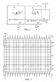
- FIG. 6 is a circuit diagram illustrating a circuit for performing the simulation. It has the same construction as shown in FIG. 3 , except that current sources I 1 and I 2 are replaced with more realistic current mirror transistor circuits.
- the simulation test defines the linearity. The slope of the output curve at an input reference voltage (2.7 V) is determined plotting a curve having the desired slope passing through the point of the reference voltage.
- the linearity error is defined as the proportion of deviation from the aforementioned obtained straight line (theoretical value), and it is defined by following equation (11).
- the linearity error is a function of input voltage V in .
- the linearity error tends to increase as the input voltage deviates from the reference voltage.
- FIG. 7( a ) shows output (V) versus input (V) of the CMOS image sensor in the present embodiment and that in the prior art.
- Curve (a) shows the input-output curve in the this embodiment compared with straight line (a i ) as its theoretical value.
- Curve (b) shows the input-output curve of the prior art compared with straight line (b i ) as its theoretical value.
- FIG. 7( b ) shows the linearity error of output (V) versus input (V) for CMOS image sensors in the present embodiment and in the prior art.
- Curve (a) shows the linearity error of the present embodiment.
- Curve (b) shows the linearity error in the prior art.
- FIG. 7( b ) shows the linearity error varies corresponding to the input value in the prior art.
- FIG. 7( b ) also shows the dependence of the linearity error on the input value is smaller in the present embodiment. In the operation region where a bias current source operates, the linearity error is approximately 0 with high stability.
- equation (8) indicates correction should be made so that V th1 is approximately V th2 .
- V 1in is shown by equation (12).
- V in V FD +[V th2 ⁇ V out ⁇ V th1 ⁇ V out ⁇ ] (12)
- FIG. 8( a ) shows output (V) versus input (V) of CMOS image sensors in the present embodiment and in the prior art.
- Curve (a) shows the input-output curve in the present embodiment.
- Curve (b) shows the input-output curve of the prior art.
- FIG. 8( b ) shows the linearity error of output (V) versus input (V) of CMOS image sensors in the present embodiment and in the prior art.
- Curve (a) shows the linearity error in the present embodiment.
- Curve (b) shows the linearity error straight line in the prior art.
- FIG. 9( a ) shows the output (V) versus the input (V) of CMOS image sensors in the present embodiment and in the prior art.
- Curve (a) shows the input-output curve in the present embodiment.
- Curve (a 1 ) corresponds to a gain of 10 ⁇
- (a 2 ) corresponds to a gain of 100 ⁇
- curve (a 3 ) corresponds to a gain of 1000 ⁇
- curve (a 4 ) corresponds to a gain of 10,000 ⁇ .
- Curve (b) shows the input-output curve in the prior art.
- FIG. 9( b ) shows the linearity error of output (V) versus input (V) of CMOS image sensors in the present embodiment and in the prior art.
- Curve (a) shows the linearity error in the present embodiment.
- Curve (a 1 ) corresponds to a gain of 10 ⁇
- curve (a 2 ) corresponds to a gain of 100 ⁇
- curve (a 3 ) corresponds to a gain of 1000 ⁇
- curve (a 4 ) corresponds to a gain of 10,000 ⁇ .
- Curve (b) shows the linearity error straight line in the prior art.
- FIG. 10( a ) shows output (V) versus input (V) of CMOS image sensors in the present embodiment and in the prior art.
- Curve (a) shows the input-output curve of the present embodiment. Curve (a 1 ) corresponds to ⁇ 15° C., curve (a 2 ) corresponds to 27° C., and curve (a 3 ) corresponds to 80° C.
- Curve (b) shows the input-output curve in the prior art. Curve (b 1 ) corresponds to ⁇ 15° C., curve (b 2 ) corresponds to 27° C., and curve (b 3 ) corresponds to 80° C.
- FIG. 10( b ) shows the linearity error of output (V) versus input (V) of the CMOS image sensors in the present embodiment and in the prior art.
- Curve (a) shows the linearity error of the present embodiment. Curve (a 1 ) corresponds to ⁇ 15° C., curve (a 2 ) corresponds to 27° C., and curve a 3 corresponds to 80° C.
- Curve (b) shows the linearity error straight line in the prior art. Curve (b 1 ) corresponds to ⁇ 15° C., curve (b 2 ) corresponds to 27° C. and curve (b 3 ) corresponds to 80° C.
- the value of the output varies as a function of the temperature increasing the dispersion.
- the dispersion in output with respect to variation in temperature is small improving the linearity.
- CMOS image sensor The linearity of a CMOS image sensor is extremely important. If the linearity is not good, ⁇ compensation and other post-treatments should be performed for each integrated circuit. This requires a longer testing time and a higher cost. Because the compensation parameters depend on the temperature, it is extremely difficult to perform temperature dependent compensation. In order to obtain a wide dynamic range with a CMOS image sensor in the present embodiment, it is necessary to switch between a high-gain output and a low-gain output. Consequently, if highly reliable linearity is absent in the output of each color of RGB, color drift occurs significantly degrading the image quality.
- the present invention solves these problems by forming compensating circuits containing compensating transistors on the same substrate as the image pixels.
- the compensating transistor compensated for the variation in the threshold due to a back gate effect to improve the linearity independent of the input voltage.
- the value of the gain being the magnitude of the output value with respect to the input value can in theory be increased to one, thus no gain loss is possible.
- the compensating transistors are formed in the same manufacturing process and on the same substrate as the pixels, matching is high. Even if the outside temperature varies, because the two transistors are driven at nearly the same temperature the influence of temperature is hardly felt. Because the integrated circuit output can be compensated for linearity on board, a later stage of correction is not needed. Thus the testing time and cost are reduced. This is also an advantage.
- pixels PX and compensating pixels CC are set adjacent to each other and have the same structure in order to compensate for linearity at high precision. It is preferred that the compensating transistors be set near the amplification transistors in the image pixels. It is preferred that the compensating transistors and the amplifiers be set with a certain spacing between them in order to match the plural amplifiers. For example, it is preferred that dummy pixels DC of 2 or 3 pixels be set between compensating pixel CC and the amplifier. The present invention is not limited to this scheme.
- the solid-state image pickup device includes additive capacitance elements giving the pixels a wide dynamic range.
- the present invention is not limited to this scheme.
- This invention may also be used in a solid-state image pickup device with a conventional dynamic range without additive capacitance elements. Even using additive capacitance elements in the pixels, the ratio of the capacitance of the floating diffusion to that of additive capacitance elements can still be selected appropriately corresponding to the design.
- This invention is not limited to a CMOS image sensor.
- the compensating circuit of this invention may also be used in the read mechanism that converts the charge of each pixel to a voltage.
- compensating pixel CC and pixel PX are the same.
- the compensating transistor in compensating pixel CC corresponds to the amplification transistor in pixel PX effects the output operation.
- the compensating pixel CC may be constructed in which other elements, such as diodes, etc., are not included and may be deleted.
- the diffusion region in compensating pixel CC may be formed in the same way as in pixel PX and a metal layer not formed.
- dummy pixel DC may be disposed adjacent to pixel PX and compensating pixel CC disposed adjacent to dummy pixel DC.
- the construction may have dummy pixel DC disposed between pixel PX and compensating pixel CC.
- the solid-state image pickup device of the present invention can be adopted in a CMOS image sensor, CCD image sensor, and other solid-state image pickup devices in a digital camera, a camera-attached cell phone, etc.
Landscapes
- Engineering & Computer Science (AREA)
- Multimedia (AREA)
- Signal Processing (AREA)
- Solid State Image Pick-Up Elements (AREA)
- Transforming Light Signals Into Electric Signals (AREA)
Abstract
Description
q is the elementary charge; ∈Si is the dielectric constant of silicon; Nsub is impurity concentration in the substrate; Cox is the capacitance of the gate oxide film; ni is the true carrier density; k is the Boltzmann constant; and T represents the absolute temperature.
V out1 =V in −V th1 {V out1} (4)
A(V out1 −V out2)=V out2 +V th1 {V out2} (5)
V out2 ≈V out1 for (A→∞) (7)
V in =V FD +[V th2 {V out }−V th1 {V out}] (12)
Claims (17)
Applications Claiming Priority (2)
| Application Number | Priority Date | Filing Date | Title |
|---|---|---|---|
| JP2007301122A JP4480753B2 (en) | 2007-11-21 | 2007-11-21 | Solid-state imaging device |
| JP2007-301122 | 2007-11-21 |
Publications (2)
| Publication Number | Publication Date |
|---|---|
| US20090128679A1 US20090128679A1 (en) | 2009-05-21 |
| US8054358B2 true US8054358B2 (en) | 2011-11-08 |
Family
ID=40641516
Family Applications (1)
| Application Number | Title | Priority Date | Filing Date |
|---|---|---|---|
| US12/275,681 Active 2030-01-14 US8054358B2 (en) | 2007-11-21 | 2008-11-21 | Solid state image pickup device |
Country Status (2)
| Country | Link |
|---|---|
| US (1) | US8054358B2 (en) |
| JP (1) | JP4480753B2 (en) |
Cited By (3)
| Publication number | Priority date | Publication date | Assignee | Title |
|---|---|---|---|---|
| US20120273655A1 (en) * | 2011-04-26 | 2012-11-01 | Canon Kabushiki Kaisha | Image sensing apparatus and control method thereof |
| US20130127515A1 (en) * | 2011-11-22 | 2013-05-23 | Taiwan Semiconductor Manufacturing Company, Ltd. | Voltage dividing circuit |
| US20170214872A1 (en) * | 2016-01-22 | 2017-07-27 | Panasonic Intellectual Property Management Co., Ltd. | Imaging device |
Families Citing this family (5)
| Publication number | Priority date | Publication date | Assignee | Title |
|---|---|---|---|---|
| JP6150457B2 (en) * | 2011-05-12 | 2017-06-21 | キヤノン株式会社 | Solid-state imaging device, driving method for solid-state imaging device, and solid-state imaging system |
| JP6137997B2 (en) * | 2012-10-31 | 2017-05-31 | ルネサスエレクトロニクス株式会社 | Solid-state imaging device |
| JP7072362B2 (en) * | 2017-09-26 | 2022-05-20 | ブリルニクス シンガポール プライベート リミテッド | Solid-state image sensor, solid-state image sensor driving method, and electronic equipment |
| WO2019188729A1 (en) * | 2018-03-27 | 2019-10-03 | 株式会社Imaging Device Technologies | Image sensor |
| US12069391B2 (en) * | 2021-07-29 | 2024-08-20 | Omnivision Technologies, Inc. | Readout architectures for dark current reduction in indirect time-of-flight sensors |
Citations (11)
| Publication number | Priority date | Publication date | Assignee | Title |
|---|---|---|---|---|
| JPH0590556A (en) | 1990-05-11 | 1993-04-09 | Olympus Optical Co Ltd | Solid-state image pick-up element |
| JP2000165754A (en) | 1998-11-27 | 2000-06-16 | Canon Inc | Solid-state imaging device and signal reading method of solid-state imaging device |
| JP2002077737A (en) | 2000-06-14 | 2002-03-15 | Nec Corp | Image sensor |
| US20020134918A1 (en) * | 2001-02-19 | 2002-09-26 | Takashi Miida | Changeable gain amplifier, solid-state imaging device and optical signal reading method |
| JP2003134396A (en) | 2001-10-29 | 2003-05-09 | Canon Inc | Imaging device, driving method of imaging device, radiation imaging apparatus using the imaging device, and radiation imaging system using the same |
| US6831685B1 (en) * | 1998-05-27 | 2004-12-14 | Canon Kabushiki Kaisha | Solid-state image pickup element |
| JP2005083790A (en) | 2003-09-05 | 2005-03-31 | Tamron Co Ltd | Laser level |
| JP2005328493A (en) | 2004-04-12 | 2005-11-24 | Shigetoshi Sugawa | Solid-state imaging device, optical sensor, and operation method of solid-state imaging device |
| JP2006217410A (en) | 2005-02-04 | 2006-08-17 | Tohoku Univ | Optical sensor and solid-state imaging device |
| US20080062296A1 (en) * | 2006-09-07 | 2008-03-13 | Canon Kabushiki Kaisha | Photoelectric conversion device and imaging device |
| US20080303058A1 (en) * | 2007-06-07 | 2008-12-11 | Mitsuyoshi Mori | Solid state imaging device and method for fabricating the same |
Family Cites Families (4)
| Publication number | Priority date | Publication date | Assignee | Title |
|---|---|---|---|---|
| JP3128012B2 (en) * | 1991-10-15 | 2001-01-29 | キヤノン株式会社 | Photoelectric conversion device |
| JP4274533B2 (en) * | 2003-07-16 | 2009-06-10 | キヤノン株式会社 | Solid-state imaging device and driving method thereof |
| JP4474982B2 (en) * | 2004-04-19 | 2010-06-09 | ソニー株式会社 | Solid-state imaging device and signal processing method for solid-state imaging device |
| JP4455215B2 (en) * | 2004-08-06 | 2010-04-21 | キヤノン株式会社 | Imaging device |
-
2007
- 2007-11-21 JP JP2007301122A patent/JP4480753B2/en active Active
-
2008
- 2008-11-21 US US12/275,681 patent/US8054358B2/en active Active
Patent Citations (11)
| Publication number | Priority date | Publication date | Assignee | Title |
|---|---|---|---|---|
| JPH0590556A (en) | 1990-05-11 | 1993-04-09 | Olympus Optical Co Ltd | Solid-state image pick-up element |
| US6831685B1 (en) * | 1998-05-27 | 2004-12-14 | Canon Kabushiki Kaisha | Solid-state image pickup element |
| JP2000165754A (en) | 1998-11-27 | 2000-06-16 | Canon Inc | Solid-state imaging device and signal reading method of solid-state imaging device |
| JP2002077737A (en) | 2000-06-14 | 2002-03-15 | Nec Corp | Image sensor |
| US20020134918A1 (en) * | 2001-02-19 | 2002-09-26 | Takashi Miida | Changeable gain amplifier, solid-state imaging device and optical signal reading method |
| JP2003134396A (en) | 2001-10-29 | 2003-05-09 | Canon Inc | Imaging device, driving method of imaging device, radiation imaging apparatus using the imaging device, and radiation imaging system using the same |
| JP2005083790A (en) | 2003-09-05 | 2005-03-31 | Tamron Co Ltd | Laser level |
| JP2005328493A (en) | 2004-04-12 | 2005-11-24 | Shigetoshi Sugawa | Solid-state imaging device, optical sensor, and operation method of solid-state imaging device |
| JP2006217410A (en) | 2005-02-04 | 2006-08-17 | Tohoku Univ | Optical sensor and solid-state imaging device |
| US20080062296A1 (en) * | 2006-09-07 | 2008-03-13 | Canon Kabushiki Kaisha | Photoelectric conversion device and imaging device |
| US20080303058A1 (en) * | 2007-06-07 | 2008-12-11 | Mitsuyoshi Mori | Solid state imaging device and method for fabricating the same |
Cited By (6)
| Publication number | Priority date | Publication date | Assignee | Title |
|---|---|---|---|---|
| US20120273655A1 (en) * | 2011-04-26 | 2012-11-01 | Canon Kabushiki Kaisha | Image sensing apparatus and control method thereof |
| US20130127515A1 (en) * | 2011-11-22 | 2013-05-23 | Taiwan Semiconductor Manufacturing Company, Ltd. | Voltage dividing circuit |
| US20170214872A1 (en) * | 2016-01-22 | 2017-07-27 | Panasonic Intellectual Property Management Co., Ltd. | Imaging device |
| US10225500B2 (en) * | 2016-01-22 | 2019-03-05 | Panasonic Intellectual Property Management Co., Ltd. | Imaging device including output signal lines for each column |
| US10999542B2 (en) | 2016-01-22 | 2021-05-04 | Panasonic Intellectual Property Management Co., Ltd. | Imaging device including lines for each column |
| US11438536B2 (en) | 2016-01-22 | 2022-09-06 | Panasonic Intellectual Property Management Co., Ltd. | Imaging device including lines for each column |
Also Published As
| Publication number | Publication date |
|---|---|
| US20090128679A1 (en) | 2009-05-21 |
| JP2009130479A (en) | 2009-06-11 |
| JP4480753B2 (en) | 2010-06-16 |
Similar Documents
| Publication | Publication Date | Title |
|---|---|---|
| US8054358B2 (en) | Solid state image pickup device | |
| CN107770461B (en) | Solid-state imaging device, driving method of solid-state imaging device, and electronic device | |
| US7903150B2 (en) | Differential amplifier circuit used in solid-state image pickup apparatus, and arrangement that avoids influence of variations of integrated circuits in manufacture and the like | |
| KR100572206B1 (en) | DC offset and gain correction method and system for CMOS image sensor | |
| US8368790B2 (en) | Image sensing apparatus and imaging system | |
| JP3466886B2 (en) | Solid-state imaging device | |
| KR100555609B1 (en) | CMOS Image Sensor with Improved Curve Factor | |
| KR100555608B1 (en) | CMOS image sensor with fixed pattern noise reduction | |
| US7808537B2 (en) | Photoelectric conversion apparatus with fully differential amplifier | |
| US9105553B2 (en) | Solid-state imaging apparatus with plural current source circuits | |
| US9066031B2 (en) | Solid-state imaging device and imaging apparatus | |
| US8159581B2 (en) | Photoelectric conversion device and image pickup system using the photoelectric conversion device | |
| TW200810544A (en) | Solid state imaging device and imaging device | |
| US7772537B2 (en) | Linear distributed pixel differential amplifier having mirrored inputs | |
| CN102428695A (en) | Image capturing apparatus, image capturing system, and method of driving image capturing apparatus | |
| KR20080019182A (en) | Solid-state imaging device | |
| US8471189B2 (en) | CMOS linear voltage/current dual-mode imager | |
| JP2013051527A (en) | Solid-state imaging device and imaging apparatus | |
| KR20030007139A (en) | Image pick up apparatus | |
| US20110279720A1 (en) | Solid-state imaging device and camera | |
| US20090295966A1 (en) | Solid-state imaging device and camera | |
| US7791660B2 (en) | Solid-state image sensing device and image sensing device | |
| US6833869B1 (en) | Solid-state imaging device with voltage followers formed by selected row transistors and column transistors | |
| US7638749B2 (en) | Capacitive transimpedance amplifier for CCD arrays | |
| CN114902653B (en) | Solid-state imaging device and amplifier array |
Legal Events
| Date | Code | Title | Description |
|---|---|---|---|
| AS | Assignment |
Owner name: TEXAS INSTRUMENTS INCORPORATED, TEXAS Free format text: ASSIGNMENT OF ASSIGNORS INTEREST;ASSIGNORS:SAWADA, HIROKAZU;TEJADA, JOSE;REEL/FRAME:022171/0083;SIGNING DATES FROM 20090121 TO 20090125 Owner name: TEXAS INSTRUMENTS INCORPORATED, TEXAS Free format text: ASSIGNMENT OF ASSIGNORS INTEREST;ASSIGNORS:SAWADA, HIROKAZU;TEJADA, JOSE;SIGNING DATES FROM 20090121 TO 20090125;REEL/FRAME:022171/0083 |
|
| STCF | Information on status: patent grant |
Free format text: PATENTED CASE |
|
| FPAY | Fee payment |
Year of fee payment: 4 |
|
| MAFP | Maintenance fee payment |
Free format text: PAYMENT OF MAINTENANCE FEE, 8TH YEAR, LARGE ENTITY (ORIGINAL EVENT CODE: M1552); ENTITY STATUS OF PATENT OWNER: LARGE ENTITY Year of fee payment: 8 |
|
| MAFP | Maintenance fee payment |
Free format text: PAYMENT OF MAINTENANCE FEE, 12TH YEAR, LARGE ENTITY (ORIGINAL EVENT CODE: M1553); ENTITY STATUS OF PATENT OWNER: LARGE ENTITY Year of fee payment: 12 |