US8050352B2 - Methods and apparatus for reducing peak-to-RMS amplitude ratio in communication signals - Google Patents
Methods and apparatus for reducing peak-to-RMS amplitude ratio in communication signals Download PDFInfo
- Publication number
- US8050352B2 US8050352B2 US12/172,786 US17278608A US8050352B2 US 8050352 B2 US8050352 B2 US 8050352B2 US 17278608 A US17278608 A US 17278608A US 8050352 B2 US8050352 B2 US 8050352B2
- Authority
- US
- United States
- Prior art keywords
- amplitude
- polar
- signal
- domain
- angle
- Prior art date
- Legal status (The legal status is an assumption and is not a legal conclusion. Google has not performed a legal analysis and makes no representation as to the accuracy of the status listed.)
- Expired - Fee Related, expires
Links
- 238000000034 method Methods 0.000 title claims abstract description 22
- 238000004891 communication Methods 0.000 title description 14
- 230000009467 reduction Effects 0.000 claims abstract description 49
- 238000012937 correction Methods 0.000 claims description 39
- 230000008569 process Effects 0.000 abstract description 8
- 230000003321 amplification Effects 0.000 abstract description 4
- 238000003199 nucleic acid amplification method Methods 0.000 abstract description 4
- 238000010586 diagram Methods 0.000 description 18
- 238000013459 approach Methods 0.000 description 9
- 238000013507 mapping Methods 0.000 description 7
- 230000015556 catabolic process Effects 0.000 description 5
- 238000006731 degradation reaction Methods 0.000 description 5
- 230000003595 spectral effect Effects 0.000 description 5
- 230000007423 decrease Effects 0.000 description 4
- 230000004044 response Effects 0.000 description 4
- 238000007493 shaping process Methods 0.000 description 4
- 238000004458 analytical method Methods 0.000 description 3
- 230000008901 benefit Effects 0.000 description 3
- 230000005540 biological transmission Effects 0.000 description 3
- 230000001413 cellular effect Effects 0.000 description 3
- 230000010363 phase shift Effects 0.000 description 3
- 238000006243 chemical reaction Methods 0.000 description 2
- 230000006835 compression Effects 0.000 description 2
- 238000007906 compression Methods 0.000 description 2
- 230000000593 degrading effect Effects 0.000 description 2
- 238000013461 design Methods 0.000 description 2
- 230000000694 effects Effects 0.000 description 2
- 230000009286 beneficial effect Effects 0.000 description 1
- 230000010267 cellular communication Effects 0.000 description 1
- 230000008859 change Effects 0.000 description 1
- 238000001816 cooling Methods 0.000 description 1
- 238000001914 filtration Methods 0.000 description 1
- 230000017525 heat dissipation Effects 0.000 description 1
- 238000005259 measurement Methods 0.000 description 1
- 238000012986 modification Methods 0.000 description 1
- 230000004048 modification Effects 0.000 description 1
- 238000012545 processing Methods 0.000 description 1
- 230000003685 thermal hair damage Effects 0.000 description 1
Images


Classifications
-
- H—ELECTRICITY
- H04—ELECTRIC COMMUNICATION TECHNIQUE
- H04L—TRANSMISSION OF DIGITAL INFORMATION, e.g. TELEGRAPHIC COMMUNICATION
- H04L25/00—Baseband systems
- H04L25/02—Details ; arrangements for supplying electrical power along data transmission lines
- H04L25/03—Shaping networks in transmitter or receiver, e.g. adaptive shaping networks
- H04L25/03006—Arrangements for removing intersymbol interference
- H04L25/03343—Arrangements at the transmitter end
-
- H—ELECTRICITY
- H03—ELECTRONIC CIRCUITRY
- H03F—AMPLIFIERS
- H03F1/00—Details of amplifiers with only discharge tubes, only semiconductor devices or only unspecified devices as amplifying elements
- H03F1/32—Modifications of amplifiers to reduce non-linear distortion
- H03F1/3241—Modifications of amplifiers to reduce non-linear distortion using predistortion circuits
- H03F1/3247—Modifications of amplifiers to reduce non-linear distortion using predistortion circuits using feedback acting on predistortion circuits
-
- H—ELECTRICITY
- H03—ELECTRONIC CIRCUITRY
- H03F—AMPLIFIERS
- H03F3/00—Amplifiers with only discharge tubes or only semiconductor devices as amplifying elements
- H03F3/20—Power amplifiers, e.g. Class B amplifiers, Class C amplifiers
- H03F3/24—Power amplifiers, e.g. Class B amplifiers, Class C amplifiers of transmitter output stages
-
- H—ELECTRICITY
- H04—ELECTRIC COMMUNICATION TECHNIQUE
- H04L—TRANSMISSION OF DIGITAL INFORMATION, e.g. TELEGRAPHIC COMMUNICATION
- H04L25/00—Baseband systems
- H04L25/02—Details ; arrangements for supplying electrical power along data transmission lines
- H04L25/03—Shaping networks in transmitter or receiver, e.g. adaptive shaping networks
- H04L25/03828—Arrangements for spectral shaping; Arrangements for providing signals with specified spectral properties
- H04L25/03834—Arrangements for spectral shaping; Arrangements for providing signals with specified spectral properties using pulse shaping
-
- H—ELECTRICITY
- H04—ELECTRIC COMMUNICATION TECHNIQUE
- H04L—TRANSMISSION OF DIGITAL INFORMATION, e.g. TELEGRAPHIC COMMUNICATION
- H04L27/00—Modulated-carrier systems
- H04L27/32—Carrier systems characterised by combinations of two or more of the types covered by groups H04L27/02, H04L27/10, H04L27/18 or H04L27/26
- H04L27/34—Amplitude- and phase-modulated carrier systems, e.g. quadrature-amplitude modulated carrier systems
- H04L27/36—Modulator circuits; Transmitter circuits
- H04L27/361—Modulation using a single or unspecified number of carriers, e.g. with separate stages of phase and amplitude modulation
-
- H—ELECTRICITY
- H03—ELECTRONIC CIRCUITRY
- H03F—AMPLIFIERS
- H03F2200/00—Indexing scheme relating to amplifiers
- H03F2200/324—An amplitude modulator or demodulator being used in the amplifier circuit
-
- H—ELECTRICITY
- H03—ELECTRONIC CIRCUITRY
- H03F—AMPLIFIERS
- H03F2200/00—Indexing scheme relating to amplifiers
- H03F2200/336—A I/Q, i.e. phase quadrature, modulator or demodulator being used in an amplifying circuit
Definitions
- the present invention relates to pulse amplitude modulation and, more particularly, to a pulse amplitude modulation (PAM) signal generator capable of reducing the peak-to-RMS amplitude ratio of communication signals without spectral degradation.
- PAM pulse amplitude modulation
- the power capability of the output device in the transmitter e.g. the final amplifier
- the selection of the output device is governed as much (or more so) by the peak-power requirement as it is by the average power requirement, where the average power is typically the measurement specified directly in the specification document for a communication system.
- the selection of the output device is governed as much (or more so) by the peak-amplitude requirement as it is by the RMS-amplitude requirement.
- the output device selection requires tradeoffs between accurate reproduction of the signal on the one hand (hereinafter referred to as “communication quality”) and, on the other hand, power efficiency, power consumption, size of the output device, etc. (hereinafter referred to as “device efficiency”).
- Improving the output device efficiency, especially the power efficiency, is highly desirable since transmitters (such as those found in battery operated cellular telephone) have a limited battery source to operate the device. Additionally, improving the device efficiency is beneficial for transmitters constrained by their cooling means, so that thermal damage to the device (e.g., handheld transmitters operating with high duty cycle, or high-power transmitters in base stations in cellular telephone systems) can be prevented. For these applications and others, it is desirable to minimize the ratio between the peak amplitude (or 99 th percentile or 99.9 th percentile) and the root-mean-square (RMS) amplitude, in order to facilitate efficient power transmission.
- the peak amplitude or 99 th percentile or 99.9 th percentile
- RMS root-mean-square
- a major disadvantage of the linear amplifier approach is that it degrades the signal quality. Typically, some amount of signal quality degradation is accepted in a system design, in exchange for slightly improved power efficiency or reduced heat dissipation. Nonetheless, the conventional (linear amplifier) approach degrades both standard measures of quality, namely an in-band quality measure and an out-of-band quality measure.
- the in-band quality measure is the RMS error vector magnitude (EVM).
- EVM error vector magnitude
- RHO is the normalized cross-correlation coefficient between the transmitted signal and its ideal version. The EVM and RHO relate to the ease with which an intended receiver can extract the message from the transmitted signal. As the EVM increases above zero, or RHO decreases below one, the transmitted signal becomes increasingly distorted compared to the ideal signal. This distortion increases the likelihood that the receiver will make errors while extracting the message.
- the out-of-band quality measure is the power spectral density (PSD) of the transmitted signal, or some measure derived therefrom.
- PSD power spectral density
- the degree to which the transmitted signal interferes with other radio channels is the degree to which the transmitted signal interferes with other radio channels.
- the overall capacity of the network is reduced or limited (e.g., the number of simultaneous users is reduced or limited).
- any means of reducing the peak-to-RMS ratio must create as little interference as possible (minimal degradation to out-of-band signal quality) while simultaneously maintaining the in-band measure of signal quality (i.e., EVM or RHO) at an acceptable level.
- the conventional (linear amplifier) approach degrades both out-of-band signal quality and in-band signal quality to reduce peak-to-RMS ratio. In fact, for some signals the conventional (linear amplifier) approach is unable to maintain acceptable quality while delivering the required average power.
- PAM signal generator modifies pulse amplitude modulated signals to reduce the peak-to-RMS amplitude ratio of the signals without degrading the power spectral density (PSD) of the signals and while simultaneously maintaining the in-band measure of signal quality (i.e., EVM or RHO) at acceptable levels.
- PSD power spectral density
- a pulse amplitude modulated (PAM) signal generator includes a modulator operable to modulate a signal with a PAM baseband signal, and a pulse injector operable to form a pulse and add the formed pulse into the PAM baseband signal at a time interval in which an amplitude of the PAM baseband signal exceeds a predetermined threshold, to create a modified baseband signal.
- PAM pulse amplitude modulated
- a pulse or an extra copy of a pulse of a PAM baseband signal is generated to modify the PAM baseband signal to reduce the peak-to-RMS amplitude ratio without substantially degrading the power spectral density (PSD) of the signal.
- PSD power spectral density
- An exemplary method for generating a pulse amplitude modulated (PAM) signal includes modulating a signal with a PAM baseband signal; forming a pulse that is a copy of a pulse in the PAM baseband signal; and adding the formed pulse into the PAM baseband signal at a time interval in which an amplitude of the PAM baseband signal exceeds a predetermined threshold, to create a modified baseband signal.
- PAM pulse amplitude modulated
- peak-to-RMS amplitude ratio reduction is used to reduce the modulation bandwidths of amplitude and/or angle modulation signals in polar modulation transmitters.
- Various examples, of performing peak-to-RMS amplitude ratio reduction in the quadrature domain, the polar domain, and both the quadrature and polar domains are disclosed.
- FIG. 1 is a block diagram of a conventional pulse amplitude modulation (PAM) signal generator
- FIG. 2 is a block diagram of a PAM signal generator, according to an embodiment of the present invention.
- FIG. 3 is a block diagram of an analyzer and a modulated baseband signal z(t);
- FIG. 4 is a flow chart of steps for providing the modulated baseband signal in the vicinity of a peak-amplitude event
- FIG. 5 is a vector diagram of a modified baseband signal y(t) in the vicinity of the peak-amplitude event in FIG. 4 , illustrating how the PAM generator in FIG. 2 operates to reduce the peak-to-RMS amplitude ratio of the modulated based band signal;
- FIG. 6 is a graph of the out-of-band signal quality PSDs of the baseband and modified baseband signals z(t) and y(t);
- FIG. 7 is a graph of the in-band signal quality measure RHO versus amplitude threshold that illustrates how the peak-to-RMS amplitude reduction apparatus and methods of the present invention do not substantially degrade in-band signal quality;
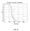
- FIG. 8 is a graph of peak-to-RMS amplitude ratios versus amplitude threshold values for various in-band signal quality measures
- FIG. 9 is a of chart of the effect of the analyzer of the PAM signal generator in FIG. 2 , in accordance with embodiments of the present invention.
- FIG. 10 is a chart illustrating an analysis process performed by the analyzer in FIG. 9 , in accordance with embodiments of the present invention.
- FIG. 11 is a block diagram of a polar modulation transmitter that is adapted to reduce the peak-to-RMS amplitude ratio of signals in the quadrature domain, according to an embodiment of the present invention
- FIG. 12 is block diagram of a quadrature domain peak-to-RMS amplitude ratio reduction circuit, which may be used to implement the quadrature domain peak-to-RMS reduction block of the polar modulation transmitter in FIG. 11 ;
- FIG. 13 is a block diagram of a polar modulation transmitter that is adapted to reduce the peak-to-RMS amplitude ratio of signals in the polar domain, according to an embodiment of the present invention
- FIG. 14 is block diagram of a polar domain peak-to-RMS amplitude ratio reduction circuit, which may be used to implement the polar domain peak-to-RMS reduction block of the polar modulation transmitter in FIG. 13 ;
- FIG. 15 is a block diagram of a polar modulation transmitter that is adapted to reduce the peak-to-RMS amplitude ratio of signals in both the quadrature domain and the polar domain, according to an embodiment of the present invention
- FIG. 16A is a diagram illustrating how the PAM signal generator in FIG. 2 or polar modulation transmitters with peak-to-RMS amplitude reduction in FIGS. 11 , 13 and 15 may be used in a wireless handset, according to an embodiment of the present invention.
- FIG. 16B is a diagram illustrating how the PAM signal generator in FIG. 2 or polar modulation transmitters with peak-to-RMS amplitude reduction in FIGS. 11 , 13 and 15 may be used in a basestation of a cellular communications network, according to an embodiment of the present invention.
- FIG. 1 is a block diagram of a conventional pulse amplitude modulation (PAM) signal generator 10 , which is well known in the prior art.
- PAM pulse amplitude modulation
- a PAM signal is a frequency-upconverted sum of amplitude-scaled, phase-shifted, and time-shifted versions of a single pulse. The amplitude-scaling and phase-shifting of the n th time-shifted version of the pulse are determined by the n th component of the digital message.
- PAM quadrature amplitude modulation
- PSK phase shift keying
- a digital message is modulated by baseband modulator 15 to form a modulated baseband signal z(t).
- the modulated baseband signal z(t) is then subjected to frequency upconversion and amplification by a frequency upconverter/amplifier 40 to produce output signal x(t) to be transmitted.
- Equation Eq. (1) describes the frequency-upconversion process used to frequency-upconvert and amplify the complex baseband signal z(t), which is also called I/Q (inphase/quadrature) representation of the signal.
- the modulated baseband signal z(t) created by the baseband modulator 15 is defined mathematically by Equation Eq. (2)
- z ⁇ ( t ) ⁇ n ⁇ a n ⁇ p ⁇ ( t - nT ) Eq . ⁇ ( 2 )
- p(t) is the pulse at time t
- T is the symbol period (1/T is the symbol rate).
- a n is the symbol corresponding to the n th component of the digital message.
- the symbol a n can be either real or complex, and can be obtained from the n th component of the digital message by means of either a fixed mapping or a time-variant mapping.
- QPSK quadrature phase shift key
- an important property of a PAM signal is that the shape of the PSD of a PAM (as a function of frequency) signal is determined exclusively by the pulse p(t), under the assumption that the symbol sequence a n has the same second-order statistical properties as white noise.
- the signal z(t) can be thought of as the output of a filter having an impulse response p(t) and being driven by a sequence of impulses with weights a n . Accordingly, the PSD S x (f) of the output signal x(t) can be shown to be equal to mathematical equation Eq. (3)
- the modulated baseband signal z(t) is modified by adding additional pulses thereto, to form new signals y(t) and ⁇ (t) defined by equations Eq. (4) and Eq. (5), respectively,
- the perturbation instances t m represent optimal times at which extra copies of the pulse p(t) are added to the modulated baseband signal z(t) to reduce the peak-to-RMS amplitude ratio of the signal.
- the perturbation instances t m define points in time at which it is desired to perturb the modulated baseband signal z(t) (e.g., whenever the amplitude of x(t) (or z(t)) exceeds some predetermined threshold).
- the threshold can be set based on any suitable criteria.
- the perturbation sequence b m represents the amplitude-scaling and phase-shifting to be applied to the pulse centered at time t m (e.g., chosen so as to reduce the amplitude of x(t) in the vicinity of time t m ).
- the second term in y(t) can be thought of as the output of a filter having impulse response p(t) and being driven by a sequence of impulses with weights b m .
- the PSDs of ⁇ (t) and x(t) will have very similar shapes (as a function of frequency).
- the PAM signal generator 100 includes a baseband modulator 115 that outputs a modulated baseband signal z(t).
- the modulated baseband signal z(t) is coupled to an input of a pulse injector 120 , which is operable to add a pulse to the modulated baseband signal z(t) at time intervals in which the signal amplitude exceeds a predetermined threshold to create a modified baseband signal y(t).
- the modulated baseband signal z(t) passes into analyzer 122 , which determines appropriate perturbation instances t m , and outputs a perturbation sequence value b m at time instant t m .
- the perturbation sequence value b m passes through a pulse-shaping filter 134 having an impulse response r(t), the output of which is added to the modulated baseband signal z(t), via adder 136 , to produce the modified baseband signal y(t).
- the modified baseband signal y(t) is passed to a frequency upconverter/amplifier 140 or any appropriate means for frequency upconversion.
- the impulse response r(t) of the pulse-shaping filter 134 can be identical to the original pulse p(t), as described above, or it can be different from p(t) (e.g., it may be a truncated version of p(t) to simplify implementation).
- the analyzer 122 includes a signal analysis unit 124 , a threshold (amplitude) detector 126 , phase angle measurer 128 , amplitude measurer 130 and amplitude-scaling and phase-shifting calculator 132 .
- the signal analysis unit 124 receives, as input, and observe the modulated baseband signal z(t).
- the threshold detector 126 detects, at step S 110 , when (the time) the threshold is exceeded in the modulated baseband signal z(t) to define the time t m , at step S 115 .
- the analyzer 122 then measures the phase angle ⁇ m via phase angle measurer 128 and amplitude c m via amplitude measurer 130 of the modulated baseband signal z(t) at the point t m . Thereafter, the analyzer 122 computes the amplitude-scaling and phase-shifting parameter b m via amplitude-scaling and phase-shifting calculator 132 , at step S 125 .
- FIG. 5 a vector signal diagram of an unperturbed modulated baseband signal z(t) is illustrated.
- the vector signal diagram plots the quadrature (imaginary) part of the modulated baseband signal z(t) versus the in-phase (real) part of the signal over a long period of time.
- the measured peak-to-RMS ratios at various percentiles are summarized in Table 1.
- FIG. 6 is a vector diagram of the modulated baseband signal z(t) during a brief time interval when the signal is near its maximum amplitude.
- the solid line depicts the signal during a brief time interval.
- the inner dashed circle represents the RMS value of the signal over all time.
- the outer dashed circle indicates the desired peak amplitude.
- the dashed line emanating from the origin intersects the signal at its point of maximum amplitude. In this example, the desired peak amplitude is 1.5 times the RMS value.
- the pulse-shaping filter 134 has a peak amplitude equal to unity, adding the signal b m r(t ⁇ t m ) to z(t) reduces the peak amplitude from c m to the desired peak amplitude d and the modified baseband signal y(t) is shown in FIG. 7 .
- the peak amplitude of the modified baseband signal y(t) is now below the desired peak amplitude as indicated by the outer dashed circle.
- the dashed line emanating from the origin indicates the location of the peak-amplitude event in z(t) prior to peak reduction.
- the out-of band signal quality of the modified baseband signal y(t) can be measured using the PSD, as shown in FIG. 8 where it is overlaid with the PSD of the original modulated baseband signal z(t).
- the two PSDs have such similar shapes that it is difficult to distinguish between the two. This demonstrates the capability of the present invention to maintain out-of-band signal quality.
- FIG. 9 illustrates the effect the PAM generator 100 of the present invention has on the in-band signal quality measure RHO.
- RHO decreases, indicating worsening in-band signal quality.
- the specification for RHO in the IS-95 standard is that RHO must exceed 0.94, over the range of desired peak amplitudes.
- the in-band signal quality is shown to be in compliance with the specification.
- a range of reductions in peak-to-RMS ratio can be obtained, as shown in FIG. 10 .
- RHO exceeds 0.98 and the peak-to-RMS ratio at the 99.9 th percentile is 4.6 dB.
- the present invention has reduced the peak-to-RMS ratio by 3.5 dB with no degradation of the out-of-band signal quality, and minimal degradation of the in-band signal quality.
- Such a large reduction in peak-to-RMS ratio facilitates improved power efficiency and/or higher average power output capability by an amplifier, as will be appreciated by those skilled in amplifier design.
- FIG. 11 is a drawing of a polar modulation transmitter 1100 which is adapted to reduce the peak-to-RMS amplitude ratio in the quadrature domain.
- the polar modulation transmitter 1100 comprises a quadrature domain peak-to-RMS reduction block 1102 ; a rectangular-to-polar converter 1104 implemented using a Coordinate Rotation Digital Computer (CORDIC) algorithm; an amplitude modulator 1106 configured in an amplitude modulation (AM) path; a phase modulator 1108 configured in a phase modulation (PM) path; a power amplifier (PA) 1110 ; and an antenna 1112 .
- CORDIC Coordinate Rotation Digital Computer
- the quadrature domain peak-to-RMS reduction block 1102 modifies in-phase (I) and quadrature phase (Q) signals received from a baseband processor (not shown) to produce modified I′ and Q′ signals having a reduced peak-to-RMS amplitude ratio.
- the CORDIC converter 1104 converts the modified I′ and Q′ from rectangular coordinates to polar coordinates, thereby producing an amplitude modulation signal ⁇ and an angle modulation signal ⁇ .
- the amplitude and phase modulation signals ⁇ and ⁇ may comprise analog waveforms, or may comprise time sampled waveforms having digital levels representing the amplitude and phase.
- the AM path of the polar modulation transmitter 1100 is configured to receive the amplitude modulation signal ⁇ containing the envelope information of the original baseband modulation.
- the amplitude modulator 1106 operates to modulate a direct current (DC) power supply signal Vsupply according to the time varying envelope information in the amplitude modulation signal ⁇ .
- the resulting amplitude modulated power supply signal is coupled to the power supply port of the PA 1110 .
- the PM path is configured to receive the angle modulation signal ⁇ , which contains the angle information of the original baseband modulation.
- the phase modulator 1108 operates to modulate a radio frequency (RF) carrier according to the time varying angle information in the angle modulation signal ⁇ .
- the resulting phase modulated RF carrier is coupled to the RF input of the PA 1110 .
- RF radio frequency
- the PA 1110 is configured to operate in its nonlinear region of operation, where it is efficient at converting DC power from the DC power supply Vsupply to RF power at the output of the PA 1110 .
- the PA 1110 is implemented as a Class D, E or F switch-mode PA 1110 operating in compression, so that the output power of the PA 1110 is directly controlled by the amplitude modulated power supply signal applied to the power supply port of the PA 1110 .
- the output of the PA 1110 is an amplitude- and phase-modulated RF carrier containing the original information-bearing modulation. After being amplified by the PA 1110 , the amplitude- and phase modulated RF carrier is fed to the antenna 1112 , which radiates the modulated RF carrier over the air to a remote receiver.
- FIG. 12 is a block diagram of a peak-to-RMS amplitude ratio reduction circuit 1200 , which may be used to implement the quadrature domain peak-to-RMS reduction block 1102 of the polar modulation transmitter 1100 in FIG. 11 .
- the peak-to-RMS amplitude ratio reduction circuit 1200 includes a main path configured to receive the I and Q signals, first and second pulse injectors 1202 and 1204 , similar to the pulse injector 120 used in the PAM signal generator 100 in FIG. 2 above.
- the first and second pulse injectors 1202 and 1204 both include a peak-to-RMS analyzer 1206 and a correction pulse generator 1208 .
- the peak-to-RMS analyzers 1206 monitor the amplitudes of the I and Q signals to determine times or time intervals in which the amplitude of either signal exceeds a predetermined threshold.
- the correction pulse generators 1208 operate to inject correction pulses in either or both the I and Q signals for the times when the amplitudes of the signals exceed the predetermined threshold.
- the correction pulses are injected into the unmodified I and Q signals in the main signal path via the first and second summers 1212 and 1214 , thereby producing the modified I′ and Q′ signals having reduced peak-to-RMS amplitude ratios.
- the delay element 1210 in the main signal path accounts for the delay needed to perform the peak-to-RMS reduction, thereby ensuring the correction pulses are combined with the unmodified I and Q signals at the appropriate times.
- Peak-to-RMS amplitude ratio reduction may also be performed in the polar domain, after the I and Q signals have been converted to polar coordinates. This approach, which is illustrated in FIG. 13 , may be advantageously used in situations where the rectangular-to-polar conversion process performed by the CORDIC converter 1104 results in substantial bandwidth expansion of the amplitude and angle modulation signals ⁇ and ⁇ .
- the polar modulation transmitter 1300 operates similar to the polar modulation transmitter 1100 in FIG. 11 , except that peak-to-RMS amplitude ratio reduction is performed by a polar domain peak-to-RMS reduction block 1302 following the CORDIC converter 1104 .
- FIG. 14 is a block diagram of a polar domain peak-to-RMS amplitude ratio reduction circuit 1400 , which may be used to implement that polar domain peak-to-RMS reduction block 1302 in the polar modulation transmitter 1300 in FIG. 13 .
- the polar domain peak-to-RMS reduction circuit 1400 includes a peak-to-RMS analyzer 1402 and correction pulse generator 1404 .
- the peak-to-RMS analyzer 1402 operates to monitor the envelope information in the amplitude modulation signal ⁇ , to determine when the amplitude exceeds a predetermined threshold.
- the pulse generator 1404 generates correction pulses that are combined with the amplitude modulation signal ⁇ in the main amplitude modulation path via a first summer 1406 , to produce a modified amplitude modulation signal ⁇ ′ representing a reduced peak-to-RMS amplitude.
- the polar domain peak-to-RMS amplitude ratio reduction circuit 1400 in FIG. 14 also includes an angle modulation bandwidth reduction block 1408 , which can be employed to reduce the bandwidth of the angle information contained in the angle modulation signal ⁇ in the PM path of the polar modulation transmitter 1300 .
- the angle modulation bandwidth reduction block 1408 generates correction pulses that reduce the bandwidth of angle information in the angle modulation signal ⁇ for angles or sample-to-sample angle changes that exceed a predetermined angle or angle change threshold.
- a nonlinear filtering technique that may be used to implement the angle modulation bandwidth reduction block 1408 is described in U.S. Pat. No. 7,054,385, which is hereby incorporated by reference.
- FIG. 15 illustrates, for example, how the quadrate domain peak-to-RMS reduction block 1102 in FIG. 11 and the polar domain peak-to-RMS reduction block 1302 in FIG. 13 are combined to provide peak-to-RMS amplitude ratio reduction both prior to and after the rectangular-to-polar conversion process performed by the CORDIC converter 11104 .
- the PAM signal generator 100 in FIG. 1 and the polar modulation transmitters 1100 , 1300 and 1500 with peak-to-RMS reduction in FIGS. 11 , 13 and 15 have application in wireless communication systems.
- CDMA code division multiple access
- OFDM offset quadrature phase shift keying
- the IS-95 standard allows so-called supplementary code channels.
- the signal to be transmitted is actually a sum of OQPSK signals.
- FIG. 16A illustrates, for example, how the PAM signal generator 100 may be configured in the transmitter 210 of a mobile handset 200 .
- one of the polar modulation transmitters 1100 , 1300 and 155 with peak-to-RMS reduction in FIG. 11 , 13 or 15 may be used to implement the transmitter 210 .
- FIG. 11B shows, another example, how the PAM generator 100 may be configured in the transmitter 260 of a basestation 250 of a cellular or other wireless communications network. Similar to the handset in FIG. 16A , one of the polar modulation transmitters 1100 , 1300 and 1500 with peak-to-RMS reduction in FIG. 11 , 13 or 15 may be alternatively used to implement the transmitter 260 of the basestation 250 .
Landscapes
- Engineering & Computer Science (AREA)
- Power Engineering (AREA)
- Computer Networks & Wireless Communication (AREA)
- Signal Processing (AREA)
- Physics & Mathematics (AREA)
- Nonlinear Science (AREA)
- Spectroscopy & Molecular Physics (AREA)
- Transmitters (AREA)
- Amplifiers (AREA)
Abstract
Description
B=gA
where g is the small-signal gain of the amplifier. As the input amplitude A increases, the actual gain of the amplifier decreases below g. Thus, the corresponding output amplitude B is not quite as large as it should be. In other words, the amplifier output is not truly proportional to the input. This effectively reduces the peak-to-RMS ratio, which in turn has the benefits of power-efficiency previously described.
x(t)=Re{gz(t)e jω,t} Eq. (1)
where Re { } denotes that real part of its complex argument; ωc=2πfc defines the radio carrier frequency in radians per second; j is the imaginary square-root of negative unity; and, g is the amplifier gain. Equation Eq. (1) describes the frequency-upconversion process used to frequency-upconvert and amplify the complex baseband signal z(t), which is also called I/Q (inphase/quadrature) representation of the signal.
where p(t) is the pulse at time t; T is the symbol period (1/T is the symbol rate). For any time instant t at which z(t) is desired, the summation is taken over all values of n at which p(t−nT) is non-negligible. Also, an is the symbol corresponding to the nth component of the digital message. The symbol an can be either real or complex, and can be obtained from the nth component of the digital message by means of either a fixed mapping or a time-variant mapping. An example of a fixed mapping occurs for quadrature phase shift key (QPSK) signals, in which the nth component of the digital message is an integer dn in the set {0, 1, 2, 3}, and the mapping is given by an=exp(jπd/2). An example of a time-variant mapping occurs for π/4-shifted QPSK which uses a modified QPSK mapping given by an=exp(jπ(n+2dn)/4); that is, the mapping depends on the time-index n, not only on the message value dn.
where P(f) is the Fourier transform of the pulse p(t); and σa 2 is the mean-square value of the symbol sequence.
b m=(d−c m)exp(jθ m) Eq. (6)
where d is the desired peak amplitude.
| TABLE 1 |
| Peak-to-RMS Ratio at Percentiles of Interest for IS-95 Reverse Channel |
| Signal Having Multiple Supplementary Code Channels |
| Percentile (%) | 99 | 99.9 | 99.99 | 100 | ||
| Peak-to-RMS (dB) | 6.5 | 8.1 | 8.8 | 9 | ||
Claims (15)
Priority Applications (1)
| Application Number | Priority Date | Filing Date | Title |
|---|---|---|---|
| US12/172,786 US8050352B2 (en) | 2007-03-14 | 2008-07-14 | Methods and apparatus for reducing peak-to-RMS amplitude ratio in communication signals |
Applications Claiming Priority (3)
| Application Number | Priority Date | Filing Date | Title |
|---|---|---|---|
| US90693107P | 2007-03-14 | 2007-03-14 | |
| US12/042,689 US7639098B2 (en) | 2007-03-14 | 2008-03-05 | Methods and apparatus for reducing peak-to-RMS amplitude ratio in communication signals |
| US12/172,786 US8050352B2 (en) | 2007-03-14 | 2008-07-14 | Methods and apparatus for reducing peak-to-RMS amplitude ratio in communication signals |
Related Parent Applications (1)
| Application Number | Title | Priority Date | Filing Date |
|---|---|---|---|
| US12/042,689 Continuation-In-Part US7639098B2 (en) | 2007-03-14 | 2008-03-05 | Methods and apparatus for reducing peak-to-RMS amplitude ratio in communication signals |
Publications (2)
| Publication Number | Publication Date |
|---|---|
| US20080304594A1 US20080304594A1 (en) | 2008-12-11 |
| US8050352B2 true US8050352B2 (en) | 2011-11-01 |
Family
ID=40095867
Family Applications (1)
| Application Number | Title | Priority Date | Filing Date |
|---|---|---|---|
| US12/172,786 Expired - Fee Related US8050352B2 (en) | 2007-03-14 | 2008-07-14 | Methods and apparatus for reducing peak-to-RMS amplitude ratio in communication signals |
Country Status (1)
| Country | Link |
|---|---|
| US (1) | US8050352B2 (en) |
Cited By (4)
| Publication number | Priority date | Publication date | Assignee | Title |
|---|---|---|---|---|
| US20090310710A1 (en) * | 2008-06-11 | 2009-12-17 | Optichron, Inc. | Crest factor reduction with phase optimization |
| US20100015932A1 (en) * | 2008-07-21 | 2010-01-21 | Matsushita Electric Industrial Co., Ltd. | Signal decomposition methods and apparatus for multi-mode transmitters |
| US10523489B1 (en) * | 2018-11-13 | 2019-12-31 | Samsung Electronics Co., Ltd. | Polar transmitter with zero crossing avoidance |
| US20210314204A1 (en) * | 2018-12-21 | 2021-10-07 | Huawei Technologies Co., Ltd. | Polar Transmitter with FeedThrough Compensation |
Families Citing this family (8)
| Publication number | Priority date | Publication date | Assignee | Title |
|---|---|---|---|---|
| GB2412512B (en) * | 2002-05-31 | 2005-11-16 | Renesas Tech Corp | A communication semiconductor integrated circuit, a wireless communication apparatus, and a loop gain calibration method |
| US8204107B2 (en) * | 2008-04-09 | 2012-06-19 | National Semiconductor Corporation | Bandwidth reduction mechanism for polar modulation |
| US8059697B2 (en) * | 2008-07-02 | 2011-11-15 | Telefonaktiebolaget L M Ericsson (Publ) | Reduced peak-to-RMS ratio multicode signal |
| US8717116B2 (en) * | 2009-12-29 | 2014-05-06 | Intel Mobile Communications GmbH | Method and apparatus for modifying a characteristic of a complex-valued signal |
| US8472559B2 (en) * | 2011-01-09 | 2013-06-25 | Mediatek Inc. | Polar transmitter and related signal transmitting method |
| US8929484B2 (en) * | 2011-07-20 | 2015-01-06 | Earl W. McCune, Jr. | Communications transmitter having high-efficiency combination modulator |
| US8736997B2 (en) * | 2012-06-13 | 2014-05-27 | HGST Netherlands B.V. | Implementing combined phase and amplitude magnetic defect detection on-the-fly |
| US10205617B2 (en) * | 2013-07-24 | 2019-02-12 | Texas Instruments Incorporated | Circuits and methods for reducing the amplitude of complex signals |
Citations (19)
| Publication number | Priority date | Publication date | Assignee | Title |
|---|---|---|---|---|
| US6041082A (en) * | 1996-09-06 | 2000-03-21 | Nec Corporation | Digital amplitude modulation amplifier and television broadcasting machine |
| US20020193085A1 (en) * | 2001-06-15 | 2002-12-19 | Telefonaktiebolaget Lm Ericsson | Systems and methods for amplification of a communication signal |
| US6931240B2 (en) * | 2002-03-19 | 2005-08-16 | Powerwave Technologies, Inc. | System and method for eliminating signal zero crossings in single and multiple channel communication systems |
| US20050281360A1 (en) * | 2001-10-22 | 2005-12-22 | Booth Richard W D | Reduction of average-to-minimum power ratio in communications signals |
| US6987417B2 (en) * | 2003-06-24 | 2006-01-17 | Northrop Grumman Corpoation | Polar and linear amplifier system |
| US20070247253A1 (en) * | 2005-12-22 | 2007-10-25 | Eoin Carey | Apparatus, system, and method for digital modulation of power amplifier in polar transmitter |
| US7358829B2 (en) * | 2005-03-22 | 2008-04-15 | Matsushita Electric Industrial Co., Ltd. | Transmission apparatus, communication apparatus and mobile radio apparatus |
| US20090004981A1 (en) * | 2007-06-27 | 2009-01-01 | Texas Instruments Incorporated | High efficiency digital transmitter incorporating switching power supply and linear power amplifier |
| US20090009243A1 (en) * | 2007-07-05 | 2009-01-08 | Matsushita Electric Industrial Co., Ltd. | Methods and Apparatus for Controlling Leakage and Power Dissipation in Radio Frequency Power Amplifiers |
| US20090023402A1 (en) * | 2005-04-26 | 2009-01-22 | Matsushita Electric Industrial Co., Ltd. | Polar modulation circuit, integrated circuit and radio apparatus |
| US20090108952A1 (en) * | 2004-06-29 | 2009-04-30 | Panasonic Corporation | Distortion compensating circuit |
| US7595702B2 (en) * | 2007-07-05 | 2009-09-29 | Panasonic Corporation | Modulation apparatus capable of correcting non-linearity of voltage controlled oscillator |
| US20090252255A1 (en) * | 2008-04-04 | 2009-10-08 | Matsushita Electric Industrial Co., Ltd. | Predistortion methods and apparatus for polar modulation transmitters |
| US20100009641A1 (en) * | 2008-07-11 | 2010-01-14 | Matsushita Electric Industrial Co.,Ltd. | Digital rf phase control in polar modulation transmitters |
| US7688157B2 (en) * | 2007-04-05 | 2010-03-30 | Panasonic Corporation | Selective envelope modulation enabling reduced current consumption |
| US7715808B2 (en) * | 2005-04-28 | 2010-05-11 | Panasonic Corporation | Polar modulating circuit, polar coordinate modulating method, integrated circuit and radio transmission device |
| US7755443B2 (en) * | 2008-02-15 | 2010-07-13 | Panasonic Corporation | Delay-based modulation of RF communications signals |
| US20100290562A1 (en) * | 2006-12-21 | 2010-11-18 | Broadcom Corporation | Digital Compensation for Nonlinearities in a Polar Transmitter |
| US7840193B2 (en) * | 2007-10-11 | 2010-11-23 | Panasonic Corporation | Transmitter and communication apparatus |
-
2008
- 2008-07-14 US US12/172,786 patent/US8050352B2/en not_active Expired - Fee Related
Patent Citations (24)
| Publication number | Priority date | Publication date | Assignee | Title |
|---|---|---|---|---|
| US6041082A (en) * | 1996-09-06 | 2000-03-21 | Nec Corporation | Digital amplitude modulation amplifier and television broadcasting machine |
| US20020193085A1 (en) * | 2001-06-15 | 2002-12-19 | Telefonaktiebolaget Lm Ericsson | Systems and methods for amplification of a communication signal |
| US7068984B2 (en) * | 2001-06-15 | 2006-06-27 | Telefonaktiebolaget Lm Ericsson (Publ) | Systems and methods for amplification of a communication signal |
| US20050281360A1 (en) * | 2001-10-22 | 2005-12-22 | Booth Richard W D | Reduction of average-to-minimum power ratio in communications signals |
| US7054385B2 (en) * | 2001-10-22 | 2006-05-30 | Tropian, Inc. | Reduction of average-to-minimum power ratio in communications signals |
| US6931240B2 (en) * | 2002-03-19 | 2005-08-16 | Powerwave Technologies, Inc. | System and method for eliminating signal zero crossings in single and multiple channel communication systems |
| US6987417B2 (en) * | 2003-06-24 | 2006-01-17 | Northrop Grumman Corpoation | Polar and linear amplifier system |
| US20090108952A1 (en) * | 2004-06-29 | 2009-04-30 | Panasonic Corporation | Distortion compensating circuit |
| US7915969B2 (en) * | 2004-06-29 | 2011-03-29 | Panasonic Corporation | Distortion compensating circuit |
| US7535310B2 (en) * | 2004-06-29 | 2009-05-19 | Panasonic Corporation | Distortion compensation circuit |
| US7358829B2 (en) * | 2005-03-22 | 2008-04-15 | Matsushita Electric Industrial Co., Ltd. | Transmission apparatus, communication apparatus and mobile radio apparatus |
| US7778612B2 (en) * | 2005-04-26 | 2010-08-17 | Panasonic Corporation | Polar modulation circuit, integrated circuit and radio apparatus |
| US20090023402A1 (en) * | 2005-04-26 | 2009-01-22 | Matsushita Electric Industrial Co., Ltd. | Polar modulation circuit, integrated circuit and radio apparatus |
| US7715808B2 (en) * | 2005-04-28 | 2010-05-11 | Panasonic Corporation | Polar modulating circuit, polar coordinate modulating method, integrated circuit and radio transmission device |
| US20070247253A1 (en) * | 2005-12-22 | 2007-10-25 | Eoin Carey | Apparatus, system, and method for digital modulation of power amplifier in polar transmitter |
| US20100290562A1 (en) * | 2006-12-21 | 2010-11-18 | Broadcom Corporation | Digital Compensation for Nonlinearities in a Polar Transmitter |
| US7688157B2 (en) * | 2007-04-05 | 2010-03-30 | Panasonic Corporation | Selective envelope modulation enabling reduced current consumption |
| US20090004981A1 (en) * | 2007-06-27 | 2009-01-01 | Texas Instruments Incorporated | High efficiency digital transmitter incorporating switching power supply and linear power amplifier |
| US7595702B2 (en) * | 2007-07-05 | 2009-09-29 | Panasonic Corporation | Modulation apparatus capable of correcting non-linearity of voltage controlled oscillator |
| US20090009243A1 (en) * | 2007-07-05 | 2009-01-08 | Matsushita Electric Industrial Co., Ltd. | Methods and Apparatus for Controlling Leakage and Power Dissipation in Radio Frequency Power Amplifiers |
| US7840193B2 (en) * | 2007-10-11 | 2010-11-23 | Panasonic Corporation | Transmitter and communication apparatus |
| US7755443B2 (en) * | 2008-02-15 | 2010-07-13 | Panasonic Corporation | Delay-based modulation of RF communications signals |
| US20090252255A1 (en) * | 2008-04-04 | 2009-10-08 | Matsushita Electric Industrial Co., Ltd. | Predistortion methods and apparatus for polar modulation transmitters |
| US20100009641A1 (en) * | 2008-07-11 | 2010-01-14 | Matsushita Electric Industrial Co.,Ltd. | Digital rf phase control in polar modulation transmitters |
Cited By (9)
| Publication number | Priority date | Publication date | Assignee | Title |
|---|---|---|---|---|
| US20090310710A1 (en) * | 2008-06-11 | 2009-12-17 | Optichron, Inc. | Crest factor reduction with phase optimization |
| US8509345B2 (en) * | 2008-06-11 | 2013-08-13 | Netlogic Microsystems, Inc. | Crest factor reduction with phase optimization |
| US20100015932A1 (en) * | 2008-07-21 | 2010-01-21 | Matsushita Electric Industrial Co., Ltd. | Signal decomposition methods and apparatus for multi-mode transmitters |
| US8489046B2 (en) * | 2008-07-21 | 2013-07-16 | Panasonic Corporation | Signal decomposition methods and apparatus for multi-mode transmitters |
| US10523489B1 (en) * | 2018-11-13 | 2019-12-31 | Samsung Electronics Co., Ltd. | Polar transmitter with zero crossing avoidance |
| US10819554B2 (en) | 2018-11-13 | 2020-10-27 | Samsung Electronics Co., Ltd. | Polar transmitter with zero crossing avoidance |
| US20210314204A1 (en) * | 2018-12-21 | 2021-10-07 | Huawei Technologies Co., Ltd. | Polar Transmitter with FeedThrough Compensation |
| US11516054B2 (en) * | 2018-12-21 | 2022-11-29 | Huawei Technologies Co., Ltd. | Polar transmitter with feedthrough compensation |
| US11943085B2 (en) | 2018-12-21 | 2024-03-26 | Huawei Technologies Co., Ltd. | Polar transmitter with feedthrough compensation |
Also Published As
| Publication number | Publication date |
|---|---|
| US20080304594A1 (en) | 2008-12-11 |
Similar Documents
| Publication | Publication Date | Title |
|---|---|---|
| US8050352B2 (en) | Methods and apparatus for reducing peak-to-RMS amplitude ratio in communication signals | |
| Zhang et al. | Design of linear RF outphasing power amplifiers | |
| KR100867548B1 (en) | Systems, methods and apparatused for linear envelope elimination and restoration transmitters | |
| US6928272B2 (en) | Distortion compensating circuit for compensating distortion occurring in power amplifier | |
| CN101090380B (en) | Systems and methods for linear envelope eliminating and recovering transmitters | |
| US8774298B2 (en) | Transmitter with adaptive back-off | |
| US20030022639A1 (en) | Peak limiter and multi-carrier amplification apparatus | |
| US8483312B2 (en) | Methods and apparatus for reducing the average-to-minimum magnitude ratio of communications signals in communications transmitters | |
| KR20040066003A (en) | An uncorrelated adaptive predistorter | |
| JP3451947B2 (en) | OFDM modulator | |
| Tavares et al. | Input back-off optimization in OFDM systems under ideal pre-distorters | |
| US8363752B2 (en) | Methods and apparatus for reducing the average-to-minimum magnitude ratio of communications signals in communications transmitters | |
| US8644424B2 (en) | Receiver apparatus, communication system, reception method and communication method | |
| US6831954B1 (en) | Apparatus, and associated method, for compensating for distortion introduced upon a send signal by an amplifier | |
| Sen et al. | Environment-adaptive concurrent companding and bias control for efficient power-amplifier operation | |
| US8385464B2 (en) | Methods and apparatus for reducing average-to-minimum power ratio in communications signals | |
| Deumal et al. | On cubic metric reduction in OFDM systems by tone reservation | |
| US8306486B2 (en) | Methods and apparatus for reducing the average-to-minimum power ratio of communications signals in communications transmitters | |
| US6515961B1 (en) | Decresting peaks in a CDMA signal | |
| Sacchi et al. | Analysis and assessment of the effects of phase noise in constant envelope multicarrier satellite transmissions | |
| US7639098B2 (en) | Methods and apparatus for reducing peak-to-RMS amplitude ratio in communication signals | |
| CN101233683B (en) | Data processing method, transmitter, device, network element and base station | |
| Sanchez et al. | System performance evaluation of power amplifier behavioural models | |
| Huang et al. | Performance of a type-based digital predistorter for solid-state power amplifier linearization | |
| Tariq et al. | Efficient implementation of pilot-aided 32 QAM for fixed wireless and mobile ISDN applications |
Legal Events
| Date | Code | Title | Description |
|---|---|---|---|
| AS | Assignment |
Owner name: MATSUSHITA ELECTRIC INDUSTRIAL CO., JAPAN Free format text: ASSIGNMENT OF ASSIGNORS INTEREST;ASSIGNORS:SCHELL, STEPHAN V.;BOOTH, RICHARD W.D.;REEL/FRAME:021395/0512;SIGNING DATES FROM 20080712 TO 20080714 Owner name: MATSUSHITA ELECTRIC INDUSTRIAL CO., JAPAN Free format text: ASSIGNMENT OF ASSIGNORS INTEREST;ASSIGNORS:SCHELL, STEPHAN V.;BOOTH, RICHARD W.D.;SIGNING DATES FROM 20080712 TO 20080714;REEL/FRAME:021395/0512 |
|
| AS | Assignment |
Owner name: PANASONIC CORPORATION, JAPAN Free format text: CHANGE OF NAME;ASSIGNOR:MATSUSHITA ELECTRIC INDUSTRIAL CO., LTD.;REEL/FRAME:022363/0306 Effective date: 20081001 Owner name: PANASONIC CORPORATION,JAPAN Free format text: CHANGE OF NAME;ASSIGNOR:MATSUSHITA ELECTRIC INDUSTRIAL CO., LTD.;REEL/FRAME:022363/0306 Effective date: 20081001 |
|
| ZAAA | Notice of allowance and fees due |
Free format text: ORIGINAL CODE: NOA |
|
| ZAAB | Notice of allowance mailed |
Free format text: ORIGINAL CODE: MN/=. |
|
| STCF | Information on status: patent grant |
Free format text: PATENTED CASE |
|
| FEPP | Fee payment procedure |
Free format text: PAYOR NUMBER ASSIGNED (ORIGINAL EVENT CODE: ASPN); ENTITY STATUS OF PATENT OWNER: LARGE ENTITY |
|
| FPAY | Fee payment |
Year of fee payment: 4 |
|
| MAFP | Maintenance fee payment |
Free format text: PAYMENT OF MAINTENANCE FEE, 8TH YEAR, LARGE ENTITY (ORIGINAL EVENT CODE: M1552); ENTITY STATUS OF PATENT OWNER: LARGE ENTITY Year of fee payment: 8 |
|
| FEPP | Fee payment procedure |
Free format text: MAINTENANCE FEE REMINDER MAILED (ORIGINAL EVENT CODE: REM.); ENTITY STATUS OF PATENT OWNER: LARGE ENTITY |
|
| LAPS | Lapse for failure to pay maintenance fees |
Free format text: PATENT EXPIRED FOR FAILURE TO PAY MAINTENANCE FEES (ORIGINAL EVENT CODE: EXP.); ENTITY STATUS OF PATENT OWNER: LARGE ENTITY |
|
| STCH | Information on status: patent discontinuation |
Free format text: PATENT EXPIRED DUE TO NONPAYMENT OF MAINTENANCE FEES UNDER 37 CFR 1.362 |
|
| FP | Lapsed due to failure to pay maintenance fee |
Effective date: 20231101 |