US8044836B2 - Continuous time sigma-delta A/D converter and electrical system comprising the A/D converter - Google Patents
Continuous time sigma-delta A/D converter and electrical system comprising the A/D converter Download PDFInfo
- Publication number
- US8044836B2 US8044836B2 US12/610,112 US61011209A US8044836B2 US 8044836 B2 US8044836 B2 US 8044836B2 US 61011209 A US61011209 A US 61011209A US 8044836 B2 US8044836 B2 US 8044836B2
- Authority
- US
- United States
- Prior art keywords
- analog
- feedback
- digital
- signal
- converter
- Prior art date
- Legal status (The legal status is an assumption and is not a legal conclusion. Google has not performed a legal analysis and makes no representation as to the accuracy of the status listed.)
- Active
Links
Images


Classifications
-
- H—ELECTRICITY
- H03—ELECTRONIC CIRCUITRY
- H03M—CODING; DECODING; CODE CONVERSION IN GENERAL
- H03M3/00—Conversion of analogue values to or from differential modulation
- H03M3/30—Delta-sigma modulation
- H03M3/322—Continuously compensating for, or preventing, undesired influence of physical parameters
- H03M3/324—Continuously compensating for, or preventing, undesired influence of physical parameters characterised by means or methods for compensating or preventing more than one type of error at a time, e.g. by synchronisation or using a ratiometric arrangement
- H03M3/344—Continuously compensating for, or preventing, undesired influence of physical parameters characterised by means or methods for compensating or preventing more than one type of error at a time, e.g. by synchronisation or using a ratiometric arrangement by filtering other than the noise-shaping inherent to delta-sigma modulators, e.g. anti-aliasing
-
- H—ELECTRICITY
- H03—ELECTRONIC CIRCUITRY
- H03M—CODING; DECODING; CODE CONVERSION IN GENERAL
- H03M3/00—Conversion of analogue values to or from differential modulation
- H03M3/30—Delta-sigma modulation
- H03M3/39—Structural details of delta-sigma modulators, e.g. incremental delta-sigma modulators
- H03M3/412—Structural details of delta-sigma modulators, e.g. incremental delta-sigma modulators characterised by the number of quantisers and their type and resolution
- H03M3/422—Structural details of delta-sigma modulators, e.g. incremental delta-sigma modulators characterised by the number of quantisers and their type and resolution having one quantiser only
- H03M3/43—Structural details of delta-sigma modulators, e.g. incremental delta-sigma modulators characterised by the number of quantisers and their type and resolution having one quantiser only the quantiser being a single bit one
-
- H—ELECTRICITY
- H03—ELECTRONIC CIRCUITRY
- H03M—CODING; DECODING; CODE CONVERSION IN GENERAL
- H03M3/00—Conversion of analogue values to or from differential modulation
- H03M3/30—Delta-sigma modulation
- H03M3/39—Structural details of delta-sigma modulators, e.g. incremental delta-sigma modulators
- H03M3/436—Structural details of delta-sigma modulators, e.g. incremental delta-sigma modulators characterised by the order of the loop filter, e.g. error feedback type
- H03M3/456—Structural details of delta-sigma modulators, e.g. incremental delta-sigma modulators characterised by the order of the loop filter, e.g. error feedback type the modulator having a first order loop filter in the feedforward path
Definitions
- the present disclosure relates to analog-to-digital converters and, particularly, to continuous time sigma-delta analog-to-digital converters.
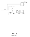
- FIG. 1 shows a conventional continuous time sigma-delta analog-to-digital converter provided with an integrator (consisting of an operational amplifier A PA and a feedback capacitor C PA ), a low pass filter F PA , a quantizer Q PA , and a feedback path via a current mode digital-to-analog converter DAC PA .
- a low unit gain bandwidth or low slew rate of the operational amplifier employed by the integrator gives rise to distortion of the feedback signal.
- the gain of the operational amplifier is too low to suppress the inherent non-linearity of its own transfer characteristic at higher frequencies, while in case of too low slew rate the gain of the operational amplifier becomes dependent on its input signal.
- the sigma-delta analog-to-digital converters of the prior art techniques require high performance integrators. Particularly, operational amplifiers showing large bandwidth and high slew rate are required.
- a continuous time sigma-delta analog-to-digital converter which comprises a summator configured to provide a difference signal equal to a difference between an input analog signal and a feedback signal; a feed-forward integrator path connected to the summator and configured to provide a digital signal; a feedback digital-to-analog converter configured to convert the digital signal into a feedback analog signal; and a feedback low pass filter structured to filter the feedback analog signal and provide the feedback signal to the summator.
- an electrical system comprising a continuous time sigma-delta analog-to-digital converter configured to produce a digital signal and a processing apparatus connected to said analog-to-digital converter and configured to process the digital signal.
- the analog-to-digital converter includes an input terminal structured to receive an input analog signal and a feedback signal; a feed-forward integrator path connected to the input terminal and configured to provide a digital signal; a feedback digital-to-analog converter configured to convert the digital signal into a feedback analog signal; and a feedback low pass filter structured to filter the feedback analog signal and provide the feedback signal to the input terminal;
- FIG. 1 schematically shows a continuous time sigma-delta analog-to-digital converter in accordance with a prior art technique
- FIG. 2 schematically shows an embodiment of an electrical system including a continuous time sigma-delta analog-to-digital converter
- FIG. 3 shows an embodiment of said continuous time sigma-delta analog-to-digital converter
- FIG. 4 shows an embodiment of a digital-to-analog converter employable by said continuous time sigma-delta analog-to-digital converter.
- FIG. 2 schematically shows an electrical system 100 such as a radio tuner system structured to receive radio broadcasts and convert them into audio-frequency signals which can be fed into an amplifier 600 driving a loudspeaker 700 .
- the radio tuner system 100 can be a highly integrated tuner which deals with transmissions using different methods of modulation or transmissions techniques, such as: FM (frequency modulation), AM (amplitude modulation) and digital audio broadcasting (DAB).
- FM frequency modulation
- AM amplitude modulation
- DAB digital audio broadcasting
- the radio tuner system 100 can be installed in a vehicle (e.g. a car) radio device.
- the radio turner system 100 comprises an analog-to-digital converter 200 (ADC) and a further analog-to-digital converter 300 (ADC), a demodulator 400 and a digital signal processor 500 (DSP).
- ADC analog-to-digital converter 200
- ADC analog-to-digital converter 300
- DSP digital signal processor 500
- each of the above analog-to-digital converter 200 and 300 is a continuous time sigma-delta analog-to-digital modulator and can be structurally and functionally analogous.
- the analog-to-digital converter 200 is configured to convert into a first digital signal the “I” component V 1in of an analog IQ signal received at an intermediate frequency.
- the further analog-to-digital converter 300 is configured to convert into a second digital signal the “Q” component V 2in of the analog IQ signal.
- the IQ demodulation is performed by the demodulator 400 which provides output digital demodulated signals to the DSP 500 for further processing.
- FIG. 3 schematically illustrates an embodiment of the continuous time sigma-delta analog-to-digital modulator 200 (hereinafter also denoted as ADC converter) which comprises a summator 1 , configured to receive an input analog signal V in (e.g. a voltage signal) and a feedback signal Vff fb , and a feed-forward integrator path 2 configured to provide a digital signal Dout on a digital output 12 .
- ADC converter continuous time sigma-delta analog-to-digital modulator 200
- the ADC converter 200 further includes a feedback path provided with a digital-to-analog converter 3 (DAC), configured to convert the digital signal Dout into a feedback analog signal V fb , and a feedback low pass filter 4 structured to filter the feedback analog signal V fb and provide the feedback signal V ffb to the summator 1 .
- the summator 1 comprises a first terminal 6 for receiving the feedback signal Vff fb , a second terminal 7 for receiving the input analog signal V in which can be, according to the system 100 of FIG. 2 , the I′′ component V 1in and a third terminal 8 .
- the feed-forward integrator path 2 comprises an integrator device including an operational amplifier in an integrator configuration.
- the integrator device includes an operational amplifier 5 provided with an inverting input “ ⁇ ” connected to the first terminal 6 of the summator 1 , a non-inverting input “+” connected to a ground terminal GND and the third terminal 8 of the summator 1 via input capacitor C P1 , and an amplifier output 9 .
- the summator 1 includes a first input resistor R P1 connected between the second terminal 7 and a the third terminal 8 , and a second input resistor R P2 connected between the third terminal 8 and the inverting input of the operational amplifier 5 .
- the feed-forward integrator path 2 also includes a feedback capacitor C having a first terminal connected to the amplifier output 9 and a second terminal connected to the inverting input of the operational amplifier 5 via an electrical link.
- This electrical link can be a conductive path or, in accordance with the illustrated embodiment, it can also include a feedback resistor R Z which is so interposed between the feedback capacitor C and the inverting input of the operational amplifier 5 .
- the feed-forward integrator path 2 includes the above mentioned second input resistor R P2 and a low pass filter 10 having a respective input connected to the amplifier output 5 and a respective output connected to a quantizer 11 .
- the above described embodiment of the ADC converter 200 can be integrated in a semiconductor chip by employing, as an example, the CMOS (complementary metal oxide semiconductor) technology or a BiCMOS (Bipolar CMOS) technology.
- CMOS complementary metal oxide semiconductor
- BiCMOS Bipolar CMOS
- a signal representing the difference between the input analog signal V in and the feedback signal V ffb is supplied.
- the operational amplifier 5 which is in the above described integrator configuration, accumulates or sums this difference and feeds an integrated analog signal to the low pass filter 10 .
- the integrated and filtered analog signal is then supplied to the quantizer 11 which via a sampling and a quantization produces the digital signal Dout.
- the frequency signal f CLK supplied to the quantizer 11 determines the data rate of the digital signal Dout, which represents the input analog signal V in plus highpass shaped quantization noise.
- the digital signal Dout is then fed to the digital-to-analog converter 3 generating the corresponding feedback analog signal V fb which can correspond to rectangular current pulses or exponentially decaying current pulses.
- the feedback analog signal V fb is then filtered by the feedback low pass filter 4 which suppresses high frequency components carried by the feedback analog signal V fb so as to produce the feedback signal V ffb .
- This feedback signal V ffb forces the digital signal Dout exiting the ADC converter 200 to track the average of the input analog signal V in .
- electrical parameters such as, capacitances and resistances
- electrical components i.e. resistors and capacitors
- the additional zero z has the effect of compensating the pole p expressed by expression (1) so as to obtain a satisfying loop stability of the ADC converter and a noise transfer function NTF comparable to the ones associated to the prior art solution above described.
- the poles p P and p can be designed to show frequencies that are far outside the usable frequency band range of the ADC converter 200 .
- the pole p P could be placed at frequency of 4 MHz.
- OSR oversampling ratio
- the digital-to-analog converter 3 of FIG. 3 can be a pulse width modulator, a binary weighted digital-to-analog converter, a ladder network digital-to-analog converter or another type of suitable digital-to-analog converter.
- the digital-to-analog converter 3 can be a ladder network converter operating in the current mode.
- the current mode technique allows the digital-to-analog converter 3 tolerating voltage swing on its output due to the passive pole p.
- a base terminal of the first current steering transistor T 1 is configured to receive the digital signal Dout (indicated in FIG. 4 as signal Dout+) to be converted in analog form, while a base terminal of the second current steering transistor T 2 is configured to receive the opposite of the digital signal Dout, i.e. an inverted digital signal Dout ⁇ .
- the collector terminal of the first current steering transistor T 1 is structured to provide an analog current signal I+ representing the result of the digital-to-analog conversion of the digital signal Dout; the collector terminal of the second current steering transistor T 2 is structured to provide the a further analog current signal I ⁇ , i.e. the result of the conversion of the inverted digital signal Dout ⁇ .
- the described embodiment of the digital-to-analog converter 3 also includes a shaping filter circuit comprising a shaping resistor R DAC connected in series to a shaping capacitor C DAC placed between an input inverter 15 and the anode of the diode 14 .
- a clock signal CLK can be fed.
- the analog-to-digital converter 200 including the digital-to-analog converter 3 of FIG. 4 is designed to produce a digital signal Dout+/ ⁇ having a high level which is several hundred mV (e.g. 500 mV) smaller than two times the diode forward voltage associated with diode 14 , while the low level of the digital signal Dout+/ ⁇ is an additional 200 mV smaller than the high level. This allows avoiding a quiescent current in the diode 14 and one of both first and second current steering transistors T 1 and T 2 .
- the voltage level associated with the digital signals Dout+/Dout ⁇ selectively switches off/on the first/second current steering transistors T 1 /T 2 so generating a corresponding current pulse I+/I ⁇ .
- the shaping resistor R DAC and the shaping capacitor C DAC defining a time constant R DAC C DAC , have a shaping effect which shapes the analog current pulse associated with the analog currents I+/I ⁇ to obtain either an exponential decaying shape if RDACCDAC ⁇ 1/fCLK or a nearly rectangular pulse if RDACCDAC>>1/fCLK.
- static high side current sources or a complementary high side structure can be added to the digital-to analog converter 16 to avoid residual static common mode currents.
- the transitions of the digital signal Dout+/Dout ⁇ are preferably timed during the low level of the clock signal CLK when both first and second current steering transistors T 1 and T 2 are switched off.
- the one-bit return-to-zero converter 16 above described allows a large voltage swing at its output, while still providing a low noise output current due to the large degeneration via the shaping resistor R DAC . Furthermore, the amount of charge that is injected is independent of the duty cycle of the clock signal CLK, because the charge that is stored in the shaping capacitor C DAC during the lowphase of the clock signal CLK is equal to the charge that is removed from the shaping capacitor C DAC during the clock high phase. This allows designing the ADC converter 200 with a loop gain which is fully independent from the duty cycle of the clock signal CLK.
- the digital-to-analog converter 3 includes an additional one-bit return-to-zero converter analogous to the one described with reference to FIG. 4 , driven by the same output digital signal Dout+/Dout ⁇ but adapted to be timed by another clock signal having opposite polarity of the clock signal CLK.
- the output current pulses I+/I ⁇ of the one-bit return-to-zero converter 16 and the additional one-bit return-to-zero converter are added.
- RDACCDAC>>1/fCLK the two combined return-to-zero converters are in this way equivalent to one non-return-to-zero converter.
- the described continuous time sigma-delta analog-to-digital converter allows employing operational amplifiers showing relaxed performances in comparison with the ones required by the sigma-delta analog-to-digital converter of the prior art.
Landscapes
- Engineering & Computer Science (AREA)
- Theoretical Computer Science (AREA)
- Compression, Expansion, Code Conversion, And Decoders (AREA)
- Analogue/Digital Conversion (AREA)
Abstract
Description
p=−1/(RpCp) (1)
In the present description electrical parameters (such as, capacitances and resistances) are indicated with the same symbols employed to identify the corresponding electrical components (i.e. resistors and capacitors) in the figures.
z=−1/(RZC) (2)
By designing the concerned electrical parameters (resistances and capacitances) so as that the product RZ C is equal to product RpCp the additional zero z has the effect of compensating the pole p expressed by expression (1) so as to obtain a satisfying loop stability of the ADC converter and a noise transfer function NTF comparable to the ones associated to the prior art solution above described.
p P=−1/(CP 1(RP1//RP2)) (3)
wherein Rp1//Rp2 indicated the total resistance for parallel electric connection:
RP1//RP2=RP 1 RP2/(RP 1 +RP2)
By designing the concerned electrical parameters (resistances and capacitances) so that the further pole pP of expression (3) is equal to the pole p of expression (1), high frequency components passing in the signal transfer function STF can be avoided.
RP1=RP2=2 k Ohm; RP=RZ=1 kOhm; C=CP=CP1=40 pF.
Claims (30)
Priority Applications (2)
| Application Number | Priority Date | Filing Date | Title |
|---|---|---|---|
| US12/610,112 US8044836B2 (en) | 2009-10-30 | 2009-10-30 | Continuous time sigma-delta A/D converter and electrical system comprising the A/D converter |
| US13/280,004 US8749416B2 (en) | 2009-10-30 | 2011-10-24 | Continuous time sigma-delta A/D converter and electrical system comprising the A/D converter |
Applications Claiming Priority (1)
| Application Number | Priority Date | Filing Date | Title |
|---|---|---|---|
| US12/610,112 US8044836B2 (en) | 2009-10-30 | 2009-10-30 | Continuous time sigma-delta A/D converter and electrical system comprising the A/D converter |
Related Child Applications (1)
| Application Number | Title | Priority Date | Filing Date |
|---|---|---|---|
| US13/280,004 Continuation US8749416B2 (en) | 2009-10-30 | 2011-10-24 | Continuous time sigma-delta A/D converter and electrical system comprising the A/D converter |
Publications (2)
| Publication Number | Publication Date |
|---|---|
| US20110102222A1 US20110102222A1 (en) | 2011-05-05 |
| US8044836B2 true US8044836B2 (en) | 2011-10-25 |
Family
ID=43924828
Family Applications (2)
| Application Number | Title | Priority Date | Filing Date |
|---|---|---|---|
| US12/610,112 Active US8044836B2 (en) | 2009-10-30 | 2009-10-30 | Continuous time sigma-delta A/D converter and electrical system comprising the A/D converter |
| US13/280,004 Active 2030-07-17 US8749416B2 (en) | 2009-10-30 | 2011-10-24 | Continuous time sigma-delta A/D converter and electrical system comprising the A/D converter |
Family Applications After (1)
| Application Number | Title | Priority Date | Filing Date |
|---|---|---|---|
| US13/280,004 Active 2030-07-17 US8749416B2 (en) | 2009-10-30 | 2011-10-24 | Continuous time sigma-delta A/D converter and electrical system comprising the A/D converter |
Country Status (1)
| Country | Link |
|---|---|
| US (2) | US8044836B2 (en) |
Cited By (3)
| Publication number | Priority date | Publication date | Assignee | Title |
|---|---|---|---|---|
| US20120188107A1 (en) * | 2011-01-20 | 2012-07-26 | Ashburn Jr Michael A | Continuous-time oversampled converter having enhanced immunity to noise |
| CN104716959A (en) * | 2013-12-12 | 2015-06-17 | 联发科技股份有限公司 | Analog-to-digital conversion device and analog-to-digital conversion method |
| US9503038B2 (en) | 2013-12-12 | 2016-11-22 | Mediatek Inc. | Current controlling device and signal converting apparatus applying the current controlling device |
Families Citing this family (5)
| Publication number | Priority date | Publication date | Assignee | Title |
|---|---|---|---|---|
| US8831084B1 (en) * | 2012-09-10 | 2014-09-09 | Altera Corporation | Apparatus and method for common mode tracking in DFE adaptation |
| US9112522B2 (en) | 2013-07-02 | 2015-08-18 | Enphase Energy, Inc. | Delta conversion analog to digital converter providing direct and quadrature output |
| US20150020592A1 (en) * | 2013-07-16 | 2015-01-22 | Samsung Electro-Mechanics Co., Ltd. | Resistive type acceleration sensor |
| CN108777577A (en) * | 2018-05-18 | 2018-11-09 | 南京中感微电子有限公司 | A kind of wireless receiver circuit |
| JP2024069854A (en) * | 2022-11-10 | 2024-05-22 | 学校法人大阪産業大学 | Delta Sigma Modulator |
Citations (7)
| Publication number | Priority date | Publication date | Assignee | Title |
|---|---|---|---|---|
| US6441767B1 (en) * | 2000-11-29 | 2002-08-27 | Raytheon Company | Method and system for adjusting a threshold control in an analog-to-digital converter |
| US6781533B2 (en) * | 2001-11-15 | 2004-08-24 | Hrl Laboratories, Llc. | Optically sampled delta-sigma modulator |
| US20070040718A1 (en) * | 2005-08-20 | 2007-02-22 | Samsung Electronics Co., Ltd. | Delta-sigma modulator circuits in which DITHER is added to the quantization levels of methods of operating the same |
| US20070216562A1 (en) * | 2006-01-27 | 2007-09-20 | Montage Technology Group, Ltd. | Integrated DSP for a DC offset cancellation loop |
| US7376400B2 (en) * | 2003-09-25 | 2008-05-20 | Texas Instruments Incorporated | System and method for digital radio receiver |
| US7439885B2 (en) * | 2005-07-07 | 2008-10-21 | Broadcom Corporation | Method and system for sample rate conversion |
| US20090325632A1 (en) * | 2008-06-30 | 2009-12-31 | Simone Gambini | Loop delay compensation for continuous time sigma delta analog to digital converter |
-
2009
- 2009-10-30 US US12/610,112 patent/US8044836B2/en active Active
-
2011
- 2011-10-24 US US13/280,004 patent/US8749416B2/en active Active
Patent Citations (7)
| Publication number | Priority date | Publication date | Assignee | Title |
|---|---|---|---|---|
| US6441767B1 (en) * | 2000-11-29 | 2002-08-27 | Raytheon Company | Method and system for adjusting a threshold control in an analog-to-digital converter |
| US6781533B2 (en) * | 2001-11-15 | 2004-08-24 | Hrl Laboratories, Llc. | Optically sampled delta-sigma modulator |
| US7376400B2 (en) * | 2003-09-25 | 2008-05-20 | Texas Instruments Incorporated | System and method for digital radio receiver |
| US7439885B2 (en) * | 2005-07-07 | 2008-10-21 | Broadcom Corporation | Method and system for sample rate conversion |
| US20070040718A1 (en) * | 2005-08-20 | 2007-02-22 | Samsung Electronics Co., Ltd. | Delta-sigma modulator circuits in which DITHER is added to the quantization levels of methods of operating the same |
| US20070216562A1 (en) * | 2006-01-27 | 2007-09-20 | Montage Technology Group, Ltd. | Integrated DSP for a DC offset cancellation loop |
| US20090325632A1 (en) * | 2008-06-30 | 2009-12-31 | Simone Gambini | Loop delay compensation for continuous time sigma delta analog to digital converter |
Cited By (9)
| Publication number | Priority date | Publication date | Assignee | Title |
|---|---|---|---|---|
| US20120188107A1 (en) * | 2011-01-20 | 2012-07-26 | Ashburn Jr Michael A | Continuous-time oversampled converter having enhanced immunity to noise |
| US8570200B2 (en) * | 2011-01-20 | 2013-10-29 | Mediatek Singapore Pte. Ltd. | Continuous-time oversampled converter having enhanced immunity to noise |
| CN104716959A (en) * | 2013-12-12 | 2015-06-17 | 联发科技股份有限公司 | Analog-to-digital conversion device and analog-to-digital conversion method |
| US20150171877A1 (en) * | 2013-12-12 | 2015-06-18 | Mediatek Inc. | Analog-to-digital converting device and analog-to-digital converting method |
| EP2890015A1 (en) * | 2013-12-12 | 2015-07-01 | MediaTek, Inc | Analog-to-digital converting device |
| US9184754B2 (en) * | 2013-12-12 | 2015-11-10 | Mediatek Inc. | Analog-to-digital converting device and analog-to-digital converting method |
| US9503038B2 (en) | 2013-12-12 | 2016-11-22 | Mediatek Inc. | Current controlling device and signal converting apparatus applying the current controlling device |
| CN104716959B (en) * | 2013-12-12 | 2018-04-13 | 联发科技股份有限公司 | Analog-to-digital conversion device and analog-to-digital conversion method |
| CN108336998A (en) * | 2013-12-12 | 2018-07-27 | 联发科技股份有限公司 | Analog-to-digital conversion device and analog-to-digital conversion method |
Also Published As
| Publication number | Publication date |
|---|---|
| US20120044100A1 (en) | 2012-02-23 |
| US8749416B2 (en) | 2014-06-10 |
| US20110102222A1 (en) | 2011-05-05 |
Similar Documents
| Publication | Publication Date | Title |
|---|---|---|
| US8749416B2 (en) | Continuous time sigma-delta A/D converter and electrical system comprising the A/D converter | |
| Van Veldhoven | A triple-mode continuous-time ΣΔ modulator with switched-capacitor feedback DAC for a GSM-EDGE/CDMA2000/UMTS receiver | |
| US8570201B2 (en) | Direct feedback for continuous-time oversampled converters | |
| US7852249B2 (en) | Sigma-delta modulator with digitally filtered delay compensation | |
| US7880654B2 (en) | Continuous-time sigma-delta modulator with multiple feedback paths having independent delays | |
| Loeda et al. | A 10/20/30/40 MHz feedforward FIR DAC continuous-time $\Delta\Sigma $ ADC with robust blocker performance for radio receivers | |
| US6414615B1 (en) | Excess delay compensation in a delta sigma modulator analog-to-digital converter | |
| US8963753B2 (en) | Oversampling A/D converter | |
| van Veldhoven | A tri-mode continuous-time/spl Sigma//spl Delta/modulator with switched-capacitor feedback DAC for a GSM-EDGE/CDMA2000/UMTS receiver | |
| Pavan | Alias Rejection of Continuous-Time $\Delta\Sigma $ Modulators With Switched-Capacitor Feedback DACs | |
| Dorrer et al. | 10-bit, 3 mW continuous-time sigma-delta ADC for UMTS in a 0.12/spl mu/m CMOS process | |
| CN1853341A (en) | Mixer circuit, receiver comprising a mixer circuit, method for generating an output signal by mixing an input signal with an oscillator signal | |
| CN108336998B (en) | Analog-to-digital conversion device and analog-to-digital conversion method | |
| Yan et al. | A continuous-time/spl Sigma//spl Delta/modulator with 88dB dynamic range and 1.1 MHz signal bandwidth | |
| US7352311B2 (en) | Continuous time noise shaping analog-to-digital converter | |
| Yamamoto et al. | A 63 mA 112/94 dB DR IF Bandpass $\Delta\Sigma $ Modulator With Direct Feed-Forward Compensation and Double Sampling | |
| Colonna et al. | A 10.7-MHz self-calibrated switched-capacitor-based multibit second-order bandpass/spl Sigma//spl Delta/modulator with on-chip switched buffer | |
| Park et al. | A High Voltage Swing Dual-Band Bandpass $\Delta\Sigma $ Modulator for Mobile Base-Station | |
| US20160241424A1 (en) | Front-End System for A Radio Device | |
| Chiang et al. | Dual-band sigma-delta modulator for wideband receiver applications | |
| Jeong et al. | Efficient discrete-time bandpass sigma-delta modulator and digital I/Q demodulator for multistandard wireless applications | |
| Chu et al. | Analysis and design of high speed/high linearity continuous time delta-sigma modulator | |
| Yang et al. | Design of a 6 th-order Continuous-time Bandpass Delta-Sigma Modulator with 250 MHz IF, 25 MHz Bandwidth, and over 75 dB SNDR | |
| Ritoniemi | High speed 1-bit sigma delta modulators | |
| Xu et al. | A Continuous-Time Sigma-Delta Modulator with Compensating Transconductance Stages and RZ FIR-DAC |
Legal Events
| Date | Code | Title | Description |
|---|---|---|---|
| AS | Assignment |
Owner name: STMICROELECTRONICS DESIGN & APPLICATION GMBH, GERM Free format text: ASSIGNMENT OF ASSIGNORS INTEREST;ASSIGNOR:ZELLER, SEBASTIAN;REEL/FRAME:023490/0848 Effective date: 20091026 |
|
| STCF | Information on status: patent grant |
Free format text: PATENTED CASE |
|
| FPAY | Fee payment |
Year of fee payment: 4 |
|
| MAFP | Maintenance fee payment |
Free format text: PAYMENT OF MAINTENANCE FEE, 8TH YEAR, LARGE ENTITY (ORIGINAL EVENT CODE: M1552); ENTITY STATUS OF PATENT OWNER: LARGE ENTITY Year of fee payment: 8 |
|
| MAFP | Maintenance fee payment |
Free format text: PAYMENT OF MAINTENANCE FEE, 12TH YEAR, LARGE ENTITY (ORIGINAL EVENT CODE: M1553); ENTITY STATUS OF PATENT OWNER: LARGE ENTITY Year of fee payment: 12 |
|
| AS | Assignment |
Owner name: STMICROELECTRONICS APPLICATION GMBH, GERMANY Free format text: CHANGE OF NAME;ASSIGNOR:STMICROELECTRONICS DESIGN AND APPLICATION GMBH;REEL/FRAME:067596/0480 Effective date: 20101229 |
|
| AS | Assignment |
Owner name: STMICROELECTRONICS INTERNATIONAL N.V., SWITZERLAND Free format text: ASSIGNMENT OF ASSIGNORS INTEREST;ASSIGNOR:STMICROELECTRONICS APPLICATION GMBH;REEL/FRAME:068926/0247 Effective date: 20241009 |