US8044718B2 - Integrated programmable gain amplifier circuit and system including the circuit - Google Patents
Integrated programmable gain amplifier circuit and system including the circuit Download PDFInfo
- Publication number
- US8044718B2 US8044718B2 US12/637,091 US63709109A US8044718B2 US 8044718 B2 US8044718 B2 US 8044718B2 US 63709109 A US63709109 A US 63709109A US 8044718 B2 US8044718 B2 US 8044718B2
- Authority
- US
- United States
- Prior art keywords
- input
- amplifier
- network
- circuit
- elements
- Prior art date
- Legal status (The legal status is an assumption and is not a legal conclusion. Google has not performed a legal analysis and makes no representation as to the accuracy of the status listed.)
- Active - Reinstated, expires
Links
- 238000010295 mobile communication Methods 0.000 claims description 6
- 230000003213 activating effect Effects 0.000 claims description 5
- 239000003990 capacitor Substances 0.000 claims description 5
- 238000010586 diagram Methods 0.000 description 8
- 238000001914 filtration Methods 0.000 description 7
- 230000005540 biological transmission Effects 0.000 description 4
- 238000012986 modification Methods 0.000 description 3
- 230000004048 modification Effects 0.000 description 3
- 230000005236 sound signal Effects 0.000 description 3
- 230000003321 amplification Effects 0.000 description 2
- 238000003199 nucleic acid amplification method Methods 0.000 description 2
- 238000005070 sampling Methods 0.000 description 2
- XUIMIQQOPSSXEZ-UHFFFAOYSA-N Silicon Chemical compound [Si] XUIMIQQOPSSXEZ-UHFFFAOYSA-N 0.000 description 1
- 230000001413 cellular effect Effects 0.000 description 1
- 238000004891 communication Methods 0.000 description 1
- 230000002860 competitive effect Effects 0.000 description 1
- 230000007423 decrease Effects 0.000 description 1
- 229910052710 silicon Inorganic materials 0.000 description 1
- 239000010703 silicon Substances 0.000 description 1
Images


Classifications
-
- H—ELECTRICITY
- H03—ELECTRONIC CIRCUITRY
- H03G—CONTROL OF AMPLIFICATION
- H03G1/00—Details of arrangements for controlling amplification
- H03G1/0005—Circuits characterised by the type of controlling devices operated by a controlling current or voltage signal
- H03G1/0088—Circuits characterised by the type of controlling devices operated by a controlling current or voltage signal using discontinuously variable devices, e.g. switch-operated
-
- H—ELECTRICITY
- H03—ELECTRONIC CIRCUITRY
- H03F—AMPLIFIERS
- H03F3/00—Amplifiers with only discharge tubes or only semiconductor devices as amplifying elements
- H03F3/45—Differential amplifiers
- H03F3/45071—Differential amplifiers with semiconductor devices only
- H03F3/45076—Differential amplifiers with semiconductor devices only characterised by the way of implementation of the active amplifying circuit in the differential amplifier
- H03F3/45475—Differential amplifiers with semiconductor devices only characterised by the way of implementation of the active amplifying circuit in the differential amplifier using IC blocks as the active amplifying circuit
-
- H—ELECTRICITY
- H03—ELECTRONIC CIRCUITRY
- H03H—IMPEDANCE NETWORKS, e.g. RESONANT CIRCUITS; RESONATORS
- H03H11/00—Networks using active elements
- H03H11/02—Multiple-port networks
- H03H11/04—Frequency selective two-port networks
- H03H11/12—Frequency selective two-port networks using amplifiers with feedback
- H03H11/126—Frequency selective two-port networks using amplifiers with feedback using a single operational amplifier
-
- H—ELECTRICITY
- H03—ELECTRONIC CIRCUITRY
- H03H—IMPEDANCE NETWORKS, e.g. RESONANT CIRCUITS; RESONATORS
- H03H11/00—Networks using active elements
- H03H11/02—Multiple-port networks
- H03H11/04—Frequency selective two-port networks
- H03H11/12—Frequency selective two-port networks using amplifiers with feedback
- H03H11/1291—Current or voltage controlled filters
-
- H—ELECTRICITY
- H03—ELECTRONIC CIRCUITRY
- H03F—AMPLIFIERS
- H03F2203/00—Indexing scheme relating to amplifiers with only discharge tubes or only semiconductor devices as amplifying elements covered by H03F3/00
- H03F2203/45—Indexing scheme relating to differential amplifiers
- H03F2203/45526—Indexing scheme relating to differential amplifiers the FBC comprising a resistor-capacitor combination and being coupled between the LC and the IC
-
- H—ELECTRICITY
- H03—ELECTRONIC CIRCUITRY
- H03F—AMPLIFIERS
- H03F2203/00—Indexing scheme relating to amplifiers with only discharge tubes or only semiconductor devices as amplifying elements covered by H03F3/00
- H03F2203/45—Indexing scheme relating to differential amplifiers
- H03F2203/45594—Indexing scheme relating to differential amplifiers the IC comprising one or more resistors, which are not biasing resistor
Definitions
- the present disclosure refers to an integrated programmable gain amplifier circuit and to a system including such an integrated circuit.
- transmission and recording systems 1 are known in the field of mobile telephony voice/audio for receiving at input a microphone analog signal in order to convert it into a digital signal.
- the system includes an integrated circuit in which a programmable gain amplifier 2 (which in this configuration is commonly called pre-amplifier), an anti-aliasing filter 3 , and an analog-digital converter 4 are provided.
- the pre-amplifier 2 is of the programmable gain type, in order to adapt the dynamics of the microphone signal, depending on the particular type of microphone used, to the input dynamic of the analog-digital converter 4 .
- the gain of the pre-amplifier 2 is set during system setup in order to provide the best performing interfacing of the analog-digital converter 4 to the particular microphone model to be used in the system.
- the anti-aliasing filter 3 has the task of eliminating the spurious components of the input microphone signal that surround the sampling frequency of the analog-digital converter in order to avoid these components from being carried in the band used by the sampling operation. Such a filter 3 is therefore a low pass filter.
- the analog-digital converter 4 is provided for converting the preamplified and filtered analog microphone signal into a digital signal, for example in order to store or transmit this digital signal.
- next-generation mobile communications devices such as cellular telephone devices, for which audio performances will be required, which may be similar to those of consumer hi-fi equipments
- the need is felt for reducing the noise introduced in the digital samples by the path through the various blocks 2 , 3 , and 4 represented in the diagram of FIG. 1 .
- the present disclosure provides a circuit that provides a sufficient noise reduction while at the same time not requiring an increase in consumption and area or requiring only a relatively limited consumption and area increase.
- an integrated programmable gain amplifier integrate circuit as defined in the claims is provided.
- an integrated programmable gain amplifier circuit for receiving at an input an analog signal.
- the circuit includes an input for receiving an analog signal, the circuit comprising an operational amplifier and a gain setup network comprising resistive elements and selection elements, that are controlled to setup gain of the amplifier circuit, the gain setup network including capacitive elements, for defining, together with the resistive elements and the operational amplifier, an anti-aliasing filter of the active RC type.
- a circuit in accordance with another embodiment of the present disclosure, includes an anti-aliasing filter of the active RC type that includes an amplifier; and a gain network that includes an input network coupled to a first input of the amplifier, and a feedback network coupled between an output of the amplifier and a second input of the amplifier, the feedback network comprising a plurality of RC cells coupled in cascode, each RC cell associated with a respective selection switch to selectively couple each of the plurality of RC cells in the cascode connection.
- a mobile communications device includes an anti-aliasing filter of the active RC type that includes an amplifier; and a gain network that includes an input network coupled to a first input of the amplifier, and a feedback network coupled between an output of the amplifier and a second input of the amplifier, the feedback network comprising a plurality of RC cells coupled in cascode, each RC cell associated with a respective selection switch to selectively couple each of the plurality of RC cells in the cascode connection.
- FIG. 1 shows a block diagram of a known system for processing a microphone signal
- FIG. 2 shows a block diagram of a system for processing a microphone signal that includes an integrated amplifier and filter circuit and an analog-digital converter in accordance with the present disclosure
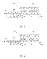
- FIG. 3 shows the circuit diagram of an integrated programmable gain amplifier and filter circuit to be used in the system of FIG. 2 ;
- FIG. 4 shows a circuit diagram of an integrated programmable gain amplifier and filter circuit to be used in the system of FIG. 2 ;
- FIG. 5 shows the circuit diagram of an integrated programmable gain amplifier and filter circuit to be used in the system of FIG. 2 ;
- FIG. 6 shows the circuit diagram of an integrated programmable gain amplifier and filter circuit to be used in the system of FIG. 2 .
- a system 20 for processing an analog signal S MC for amplifying, filtering and converting the signal S MC from analog to digital is illustrated in schematic form.
- the processing system 20 is a system for transmission or recording or both transmission and recording or receiving an analog voice/audio signal S MC .
- the analog voice/audio signal S MC is for example an analog signal provided as an output by a microphone, not shown, such as in a mobile telephone or other communication device.
- such an analog voice/audio signal S MC is in particular a differential analog signal to be provided to inputs IN P and IN N , of the processing system 20 .
- the system 20 includes an integrated programmable gain amplifier circuit 22 , for receiving at input the analog signal S MC .
- the circuit 22 includes an operational amplifier and a gain setup network 23 having resistive and selection elements, which interact with the resistive controllable elements in order to set, i.e., program, the gain of the integrated amplifier circuit 22 .
- the integrated programmable gain amplifier circuit 22 is typically called a pre-amplifier circuit.
- the gain setup network 23 also includes capacitor elements for defining, together with the resistive elements of the gain setup network and with the operational amplifier an anti-aliasing filter of the active RC type.
- the programmable gain amplifier circuit, or pre-amplifier, 22 is therefore able to output an amplified and filtered signal S AF .
- above the active RC anti-aliasing filter is a two pole low pass filter.
- the system 20 also includes an analog-digital converter 4 , which is preferably provided on the same integrated circuit of the integrated amplifier circuit 22 , for receiving at the input the amplified and filtered analog signal S AF , and providing at the output the digital samples D out , of the signal.
- the analog-digital converter 4 is a switched capacitance sigma-delta converter, for example a 16 bit converter.
- FIG. 3 a first embodiment of the integrated programmable gain amplifier circuit 22 is shown, in a particular example, wherein the circuit 22 , unlike the programmable and differential amplifier circuit 22 of FIG. 2 , is of the single-ended type.
- the integrated programmable gain amplifier circuit 22 includes an input terminal IN P for receiving at input the analog signal S MC and an output terminal OU P at which the amplifier circuit 22 provides a filtered and amplified analog signal S AF .
- the integrated amplifier circuit 22 includes an operational amplifier 33 preferably of the low noise type (operational amplifier LNA).
- the operational amplifier 33 includes an inverting input 34 , a non inverting input 35 connected to ground, and an output 36 .
- the integrated amplifier circuit 22 includes a gain setup network NRC IN , NRC F , including resistive elements, or resistors, R 1 -R 4 and Rf 1 -Rf n and selection elements S 1 -S n , which interact with the resistive elements and are controllable for example by a logic signal output by a suitable register (not shown), for setting up the gain of integrated amplifier circuit 22 .
- the selection elements S 1 -S n are preferably CMOS switches. According to a modification, the selection elements S 1 -S n are MOS switches, either re-channel (N-ch) or p-channel (P-ch).
- the gain setup network NRC IN , NRC F includes a first network NRC IN , or input network NRC IN , which is connected on the input side to the operational amplifier 33 . In this example it is connected to the inverting input 34 of operational amplifier 33 .
- a second network NRC F or feedback network, is connected between the output 36 and input 34 of operational amplifier 33 .
- the feedback network NRC F is connected between the output 36 and input 34 of operational amplifier 33 and therefore defines the feedback loop of such operational amplifier 33 .
- the selection elements S 1 -S n allow varying the ratio between the total resistance of feedback network NRC F and total resistance of input network NRC IN , therefore allowing programming the gain of amplifier circuit 22 .
- the selection elements S 1 -S n are included in the feedback network NRC F , therefore allowing the setup of value of total resistance over the feedback loop of operational amplifier 33 .
- the gain setup network NRC IN , NRC F also includes capacitor elements for defining, along with the resistive elements R 1 -R 4 and Rf 1 -Rf n and the operational amplifier 33 , an active RC anti-aliasing filter.
- an active RC anti-aliasing filter is a second order active RC filter. Therefore it can be deduced that the integrated programmable gain amplifier circuit 22 is an amplification and filtering circuit.
- the input network NRC IN includes one or more capacitor elements C 1 -C 3 and one or more resistive elements R 1 -R 4 for defining together an RC filter, more preferably a single-pole filter, provided at the input of operational amplifier 33 .
- such RC filter is of the distributed kind, so that the input network NRC IN has many RC cells, respectively (R 1 , C 1 ), (R 2 , C 2 ), and (R 3 , C 3 ), which are cascode-connected and preferably include resistive elements R 1 , R 2 , R 3 with the same resistance value and capacitor elements C 1 , C 2 , C 3 having the same capacitance.
- This allows the operational amplifier 33 to have at input a single-pole filter which is more selective with respect to the RC filter, which is only provided with a single RC cell.
- the input network NRC IN includes three cascode-connected RC cells, and a resistance R 4 connected between the last cell R 3 , C 3 and input 34 , which is an inverting input in this example, of the operational amplifier 33 .
- the feedback network NRC F includes a plurality of RC cells, which are connected in a cascode (Rf 1 , Cf 1 ), (Rf 2 , Cf 2 ), . . . , (Rf n , Cf n ) and each of them is associated with a respective selection element S 1 , . . . S n , so that selectively closing only one at a time of the selection elements S 1 , . . . S n it is possible to vary the number of RC cells that are cascode-connected between the output 36 and input 34 of operational amplifier 33 , and therefore vary the number of RC cells that define the feedback loop of the operational amplifier 33 .
- the feedback loop will only include one RC cell, i.e., the RC cell (Rf 1 , Cf 1 ) connected between the output 36 and the input 34 of the operational amplifier 33 .
- the switch by activating, i.e., closing the switch, of selection element S 2 and leaving all other selection elements S 1 and S 3 , . . .
- the feedback loop will have two cascode-connected RC cells, i.e., RC cell (Rf 1 , Cf 1 ) and cell (Rf 2 , Cf 2 ) connected between the output 36 and the input 34 of the operational amplifier 33 .
- RC cell Rf 1 , Cf 1
- the resistance and capacitance values of capacitive and resistive elements of the feedback network NRC F are defined in the design phase so that, independently from the number of RC cells (Rf 1 , Cf 1 ), (Rf 2 , Cf 2 ), . . . , (Rf n , Cf n ) which are cascode-connected between the output 36 and input 34 of operational amplifier 33 , the feedback network NRC F defines the other one of the two poles of the anti-aliasing filter, the feedback network NRC F being describable by a passive RC filter with a single pole having a substantially constant cut-off frequency. In order to achieve this, it is sufficient that in the RC cells the capacitance values are proportionally scaled with respect to the value of associated resistances.
- the cut-off frequency of the anti-aliasing filtering implemented by the integrated amplifier circuit 22 may be set at a substantially constant value with respect to a set gain variation. Based on these specifications, when the cut-off frequency of RC filter defined by the feedback network NRC F is set, and once the desired pitch and range of gain variation are defined, one skilled in the art may easily determine, in the design phase, the number of RC cells of the feedback network NRC F and the values to be selected for the capacitive and resistive elements of such network NRC F , which may be completely different from one another.
- the integrated programmable gain amplifier circuit 22 includes a feedback network NRC F having a plurality of cascode-connected RC cells, wherein at least one of the RC cells has a capacitive element, at least two resistive elements, which may be independently series-connected between the input 34 and output 36 of operational amplifier 33 by means of respective independently controllable selection elements, which are provided in the feedback network NRC F .
- NRC F feedback network having a plurality of cascode-connected RC cells, wherein at least one of the RC cells has a capacitive element, at least two resistive elements, which may be independently series-connected between the input 34 and output 36 of operational amplifier 33 by means of respective independently controllable selection elements, which are provided in the feedback network NRC F .
- the second RC cell (Rf 21 , Rf 22 , Cf 2 ) includes a capacity Cf 2 and two series connected resistors Rf 21 , Rf 22 , which may be independently connected between the input and output of operational amplifier by means of respective selection elements S 21 , S 22 in order to vary the gain of integrated programmable gain amplifier circuit 22 .
- the integrated amplifier circuit 22 of FIG. 4 in order to set the gain value, it is necessary to close only one of the selection elements S 1 , . . . S n2 .
- FIG. 5 shows an integrated programmable gain amplifier circuit 22 that is very similar to the one shown in FIG. 3 , wherein the circuit is of the fully-differential type.
- the operational amplifier 33 is of a differential type, and has two inputs 34 , 35 and two output 36 P , 36 N .
- the gain-setting network includes an input network NRC IN and two feedback networks NRC F — P and NRC F — N .
- the input network NRC IN has three cascode-connected RC cells, which are similar to those previously described, wherein, since the two inputs 34 , 35 of the operational amplifier 33 are virtual ground nodes, each of such RC cells has one capacitive element and two resistive elements.
- the input network NRC IN defines a single pole RC filter.
- Each of the two feedback networks NRC F — P and NRC F — N embodies a multi-cell single pole RC filter and the capacitive and resistive elements are defined so that the cut frequency of the anti-aliasing filtering is substantially constant with respect to a gain variation in the integrated amplifier circuit 22 .
- the integrated amplifier circuit 22 is a programmable gain integrated differential amplifier circuit, which is also an anti-aliasing differential active filter of the second order, of the low pass type. It is to be noted that in order to set the gain in the integrated circuit 22 of FIG. 5 , only one of the selection elements S 1 , . . . S n of feedback network NRC F — P has to be activated, for example by a control circuit (not shown) through a register, for example activating the selection element S 1 , and the corresponding selection element, i.e., S 1 , and only this one in the other feedback network NRC F — N .
- FIG. 6 shows a modification of amplifier circuit of FIG. 5 , wherein, in analogy to the description of the circuit of FIG. 4 , for the single-ended case, the number of capacitive elements to be provided in the feedback networks NRC F — P and NRC F — N may be reduced.
Landscapes
- Engineering & Computer Science (AREA)
- Power Engineering (AREA)
- Networks Using Active Elements (AREA)
- Amplifiers (AREA)
- Analogue/Digital Conversion (AREA)
Abstract
Description
Claims (22)
Applications Claiming Priority (2)
| Application Number | Priority Date | Filing Date | Title |
|---|---|---|---|
| ITRM2008A000664A IT1392309B1 (en) | 2008-12-15 | 2008-12-15 | INTEGRATED CIRCUIT BUILDING AMPLIFICATION CIRCUIT AND SYSTEM INCLUDING THE CIRCUIT |
| ITRM2008A000664 | 2008-12-15 |
Publications (2)
| Publication Number | Publication Date |
|---|---|
| US20100156535A1 US20100156535A1 (en) | 2010-06-24 |
| US8044718B2 true US8044718B2 (en) | 2011-10-25 |
Family
ID=41357763
Family Applications (1)
| Application Number | Title | Priority Date | Filing Date |
|---|---|---|---|
| US12/637,091 Active - Reinstated 2029-12-26 US8044718B2 (en) | 2008-12-15 | 2009-12-14 | Integrated programmable gain amplifier circuit and system including the circuit |
Country Status (3)
| Country | Link |
|---|---|
| US (1) | US8044718B2 (en) |
| EP (1) | EP2197109A1 (en) |
| IT (1) | IT1392309B1 (en) |
Cited By (10)
| Publication number | Priority date | Publication date | Assignee | Title |
|---|---|---|---|---|
| US20100323651A1 (en) * | 2009-06-23 | 2010-12-23 | Qualcomm Incorporated | Tunable adaptive filter with variable gain trans-conductance stage |
| US20110234301A1 (en) * | 2010-03-24 | 2011-09-29 | Paul Gruber | Circuit arrangement with temperature compensation |
| US20140203873A1 (en) * | 2013-01-24 | 2014-07-24 | Samsung Electronics Co., Ltd | Signal processing apparatus and method |
| US8970293B1 (en) | 2013-10-29 | 2015-03-03 | Motorola Solutions, Inc. | Active RC filter having gain-setting attenuator |
| US20160056783A1 (en) * | 2014-08-25 | 2016-02-25 | Mediatek Inc. | Resonating device with single operational amplifier |
| US20160099695A1 (en) * | 2014-10-01 | 2016-04-07 | Renesas Electronics Corporation | Semiconductor integrated circuit, variable gain amplifier, and sensing system |
| US9312879B2 (en) | 2014-08-25 | 2016-04-12 | Mediatek Inc. | Signal modulating device capable of reducing peaking in signal transfer function |
| US9419573B2 (en) * | 2014-06-27 | 2016-08-16 | Nxp, B.V. | Variable gain transimpedance amplifier |
| US9467094B2 (en) | 2014-06-27 | 2016-10-11 | Qualcomm Incorporated | Phase-dependent operational amplifiers employing phase-based frequency compensation, and related systems and methods |
| US10228797B2 (en) | 2015-09-14 | 2019-03-12 | Synaptics Incorporated | Continuous time anti-alias filter for capacitive touch sensing |
Families Citing this family (10)
| Publication number | Priority date | Publication date | Assignee | Title |
|---|---|---|---|---|
| EP2552018A1 (en) * | 2011-07-26 | 2013-01-30 | ST-Ericsson SA | Microphone preamplifier circuit |
| CN103219962B (en) * | 2013-04-15 | 2016-03-30 | 鞍钢集团矿业公司 | Programmable-gain isolating amplifier circuit and its implementation |
| US10199995B2 (en) | 2016-03-30 | 2019-02-05 | Mediatek Inc. | Programmable amplifier circuit capable of providing large or larger resistance for feedback path of its amplifier |
| CN106849903B (en) * | 2016-12-28 | 2020-12-22 | 宁波斯凯勒智能科技有限公司 | Frequency filter circuit |
| CN107317563B (en) * | 2017-08-21 | 2024-02-13 | 四川西南交大铁路发展股份有限公司 | Differential selection filter circuit and method |
| US10270407B2 (en) * | 2017-08-31 | 2019-04-23 | Core Chip Technology (Nanjing) Co., Ltd. | Programmable gain amplifier |
| CN107565921B (en) * | 2017-10-11 | 2024-04-05 | 绍兴职业技术学院 | Automatic circulation programmable amplifying circuit capable of being compared |
| JP7238269B2 (en) * | 2018-05-11 | 2023-03-14 | オムロン株式会社 | signal processing circuit |
| CN116232281B (en) * | 2023-03-13 | 2023-11-14 | 青岛艾诺仪器有限公司 | Control method of custom filter |
| WO2025251087A1 (en) * | 2024-05-31 | 2025-12-04 | The Regents Of The University Of California | Apparatus and method for low-power electrogram devices for human machine interfaces |
Citations (8)
| Publication number | Priority date | Publication date | Assignee | Title |
|---|---|---|---|---|
| EP0421423A2 (en) | 1989-10-06 | 1991-04-10 | Hitachi, Ltd. | Method of controlling filter time constant and filter circuit having the time constant control function based on the method |
| US6407658B2 (en) * | 1999-05-14 | 2002-06-18 | Koninklijke Philips Electronics N.V. | Method and arrangement for filtering with common mode feedback for low power consumption |
| US20050179505A1 (en) | 2004-02-13 | 2005-08-18 | Infineon Technologies Ag | Method and apparatus for tuning a filter |
| US20060103469A1 (en) | 2004-11-17 | 2006-05-18 | Texas Instruments Incorporated | Filter circuit providing low distortion and enhanced flexibility to obtain variable gain amplification |
| US7068108B2 (en) * | 2004-01-09 | 2006-06-27 | Texas Instruments Incorporated | Amplifier apparatus and method |
| US20070132507A1 (en) | 2005-12-13 | 2007-06-14 | Broadcom Corporation | Tuneable filters using operational amplifiers |
| US7414467B2 (en) * | 2005-11-21 | 2008-08-19 | National Semiconductor Germany Ag | Circuit configuration having a feedback, fully-differential operational amplifier |
| US7852158B2 (en) * | 2006-11-30 | 2010-12-14 | Panasonic Corporation | Operational amplifier |
-
2008
- 2008-12-15 IT ITRM2008A000664A patent/IT1392309B1/en active
-
2009
- 2009-12-14 EP EP09179092A patent/EP2197109A1/en not_active Withdrawn
- 2009-12-14 US US12/637,091 patent/US8044718B2/en active Active - Reinstated
Patent Citations (8)
| Publication number | Priority date | Publication date | Assignee | Title |
|---|---|---|---|---|
| EP0421423A2 (en) | 1989-10-06 | 1991-04-10 | Hitachi, Ltd. | Method of controlling filter time constant and filter circuit having the time constant control function based on the method |
| US6407658B2 (en) * | 1999-05-14 | 2002-06-18 | Koninklijke Philips Electronics N.V. | Method and arrangement for filtering with common mode feedback for low power consumption |
| US7068108B2 (en) * | 2004-01-09 | 2006-06-27 | Texas Instruments Incorporated | Amplifier apparatus and method |
| US20050179505A1 (en) | 2004-02-13 | 2005-08-18 | Infineon Technologies Ag | Method and apparatus for tuning a filter |
| US20060103469A1 (en) | 2004-11-17 | 2006-05-18 | Texas Instruments Incorporated | Filter circuit providing low distortion and enhanced flexibility to obtain variable gain amplification |
| US7414467B2 (en) * | 2005-11-21 | 2008-08-19 | National Semiconductor Germany Ag | Circuit configuration having a feedback, fully-differential operational amplifier |
| US20070132507A1 (en) | 2005-12-13 | 2007-06-14 | Broadcom Corporation | Tuneable filters using operational amplifiers |
| US7852158B2 (en) * | 2006-11-30 | 2010-12-14 | Panasonic Corporation | Operational amplifier |
Cited By (21)
| Publication number | Priority date | Publication date | Assignee | Title |
|---|---|---|---|---|
| US20100323651A1 (en) * | 2009-06-23 | 2010-12-23 | Qualcomm Incorporated | Tunable adaptive filter with variable gain trans-conductance stage |
| US9602079B2 (en) * | 2009-06-23 | 2017-03-21 | Qualcomm Incorporated | Tunable adaptive filter with variable gain trans-conductance stage |
| US20110234301A1 (en) * | 2010-03-24 | 2011-09-29 | Paul Gruber | Circuit arrangement with temperature compensation |
| US8446208B2 (en) * | 2010-03-24 | 2013-05-21 | Dspace Digital Signal Processing And Control Engineering Gmbh | Circuit arrangement with temperature compensation |
| US20140203873A1 (en) * | 2013-01-24 | 2014-07-24 | Samsung Electronics Co., Ltd | Signal processing apparatus and method |
| US9136808B2 (en) * | 2013-01-24 | 2015-09-15 | Samsung Electronics Co., Ltd. | Signal processing apparatus and method |
| US8970293B1 (en) | 2013-10-29 | 2015-03-03 | Motorola Solutions, Inc. | Active RC filter having gain-setting attenuator |
| US9467094B2 (en) | 2014-06-27 | 2016-10-11 | Qualcomm Incorporated | Phase-dependent operational amplifiers employing phase-based frequency compensation, and related systems and methods |
| US9419573B2 (en) * | 2014-06-27 | 2016-08-16 | Nxp, B.V. | Variable gain transimpedance amplifier |
| US20160056783A1 (en) * | 2014-08-25 | 2016-02-25 | Mediatek Inc. | Resonating device with single operational amplifier |
| US9312879B2 (en) | 2014-08-25 | 2016-04-12 | Mediatek Inc. | Signal modulating device capable of reducing peaking in signal transfer function |
| CN105375929B (en) * | 2014-08-25 | 2019-05-31 | 联发科技股份有限公司 | Resonance apparatus |
| CN105375929A (en) * | 2014-08-25 | 2016-03-02 | 联发科技股份有限公司 | Resonance apparatus |
| US9484877B2 (en) * | 2014-08-25 | 2016-11-01 | Mediatek Inc. | Resonating device with single operational amplifier |
| CN105490651A (en) * | 2014-10-01 | 2016-04-13 | 瑞萨电子株式会社 | Semiconductor integrated circuit, variable gain amplifier, and sensing system |
| US9831842B2 (en) * | 2014-10-01 | 2017-11-28 | Renesas Electronics Corporation | Semiconductor integrated circuit, variable gain amplifier, and sensing system |
| US10063201B2 (en) | 2014-10-01 | 2018-08-28 | Renesas Electronics Corporation | Semiconductor integrated circuit, variable gain amplifier, and sensing system |
| US20180342996A1 (en) * | 2014-10-01 | 2018-11-29 | Renesas Electronics Corporation | Semiconductor integrated circuit, variable gain amplifier, and sensing system |
| US20160099695A1 (en) * | 2014-10-01 | 2016-04-07 | Renesas Electronics Corporation | Semiconductor integrated circuit, variable gain amplifier, and sensing system |
| CN105490651B (en) * | 2014-10-01 | 2020-09-25 | 瑞萨电子株式会社 | Semiconductor integrated circuits, variable gain amplifiers, and sensing systems |
| US10228797B2 (en) | 2015-09-14 | 2019-03-12 | Synaptics Incorporated | Continuous time anti-alias filter for capacitive touch sensing |
Also Published As
| Publication number | Publication date |
|---|---|
| EP2197109A1 (en) | 2010-06-16 |
| US20100156535A1 (en) | 2010-06-24 |
| ITRM20080664A1 (en) | 2010-06-16 |
| IT1392309B1 (en) | 2012-02-24 |
Similar Documents
| Publication | Publication Date | Title |
|---|---|---|
| US8044718B2 (en) | Integrated programmable gain amplifier circuit and system including the circuit | |
| US6618579B1 (en) | Tunable filter with bypass | |
| US9413326B2 (en) | Second-order filter with notch for use in receivers to effectively suppress the transmitter blockers | |
| US5872475A (en) | Variable attenuator | |
| CN105409177B (en) | Analog baseband filtering device for multi-mode multi-band wireless transceiver and control method thereof | |
| US9590592B2 (en) | Configurable capacitor arrays and switched capacitor circuits | |
| CN102845079A (en) | Control of a microphone | |
| CN102916677A (en) | Infinite Impulse Response Filter and Filtering Method | |
| US8050642B2 (en) | Variable gain amplifier and receiver including the same | |
| US7098730B1 (en) | Process variation trim/tuning for continuous time filters and Δ-Σ analog to digital converters | |
| Szortyka et al. | A 42mW wideband baseband receiver section with beamforming functionality for 60GHz applications in 40nm low-power CMOS | |
| US6831506B1 (en) | Reconfigurable filter architecture | |
| D'Amico et al. | A CMOS 5 nV $/\surd $ Hz 74-dB-Gain-Range 82-dB-DR Multistandard Baseband Chain for Bluetooth, UMTS, and WLAN | |
| Abdulaziz et al. | A 3.4 mW 65nm CMOS 5 th order programmable active-RC channel select filter for LTE receivers | |
| US7984093B1 (en) | Polyphase filter having a tunable notch for image rejection | |
| WO2006117943A1 (en) | Radio filter circuit and noise reducing method | |
| Giannini et al. | Flexible baseband low-pass filter and variable gain amplifier for software defined radio front end | |
| US6906584B1 (en) | Switchable gain amplifier having a high-pass filter pole | |
| Hollman et al. | A 2.7 V CMOS dual-mode baseband filter for GSM and WCDMA | |
| US7880536B2 (en) | Simplified sallen-key low-pass filter circuit | |
| US20060279344A1 (en) | Circuit for DC offset cancellation | |
| US20090102546A1 (en) | Composite band-pass filter and method of filtering quadrature signals | |
| KR102288009B1 (en) | Image rejection complex bandpass filter | |
| CN108141222B (en) | Electronic circuits and microphones for microphones | |
| JP2005260447A (en) | Processing unit selection type signal processing device, image sensor-equipped device and communication device including the same |
Legal Events
| Date | Code | Title | Description |
|---|---|---|---|
| AS | Assignment |
Owner name: STMICROELECTRONICS S.R.L.,ITALY Free format text: ASSIGNMENT OF ASSIGNORS INTEREST;ASSIGNORS:NICOLLINI, GERMANO;NAGARI, ANGELO;REEL/FRAME:024028/0870 Effective date: 20091216 Owner name: STMICROELECTRONICS S.R.L., ITALY Free format text: ASSIGNMENT OF ASSIGNORS INTEREST;ASSIGNORS:NICOLLINI, GERMANO;NAGARI, ANGELO;REEL/FRAME:024028/0870 Effective date: 20091216 |
|
| ZAAA | Notice of allowance and fees due |
Free format text: ORIGINAL CODE: NOA |
|
| ZAAB | Notice of allowance mailed |
Free format text: ORIGINAL CODE: MN/=. |
|
| STCF | Information on status: patent grant |
Free format text: PATENTED CASE |
|
| FPAY | Fee payment |
Year of fee payment: 4 |
|
| AS | Assignment |
Owner name: STMICROELECTRONICS INTERNATIONAL NV, NETHERLANDS Free format text: ASSIGNMENT OF ASSIGNORS INTEREST;ASSIGNOR:STMICROELECTRONICS S.R.L.;REEL/FRAME:037841/0162 Effective date: 20160201 |
|
| AS | Assignment |
Owner name: FRANCE BREVETS, FRANCE Free format text: ASSIGNMENT OF ASSIGNORS INTEREST;ASSIGNOR:STMICROELECTRONICS INTERNATIONAL NV;REEL/FRAME:039140/0584 Effective date: 20160321 |
|
| MAFP | Maintenance fee payment |
Free format text: PAYMENT OF MAINTENANCE FEE, 8TH YEAR, LARGE ENTITY (ORIGINAL EVENT CODE: M1552); ENTITY STATUS OF PATENT OWNER: LARGE ENTITY Year of fee payment: 8 |
|
| AS | Assignment |
Owner name: MICROELECTRONIC INNOVATIONS, LLC, MICHIGAN Free format text: ASSIGNMENT OF ASSIGNORS INTEREST;ASSIGNOR:FRANCE BREVETS;REEL/FRAME:060161/0346 Effective date: 20220509 |
|
| AS | Assignment |
Owner name: MICROELECTRONIC INNOVATIONS, LLC, DELAWARE Free format text: CORRECTIVE ASSIGNMENT TO CORRECT THE THE ASSIGNEE ADDRESS PREVIOUSLY RECORDED AT REEL: 060161 FRAME: 0346. ASSIGNOR(S) HEREBY CONFIRMS THE ASSIGNMENT;ASSIGNOR:FRANCE BREVETS;REEL/FRAME:060389/0768 Effective date: 20220616 |
|
| FEPP | Fee payment procedure |
Free format text: MAINTENANCE FEE REMINDER MAILED (ORIGINAL EVENT CODE: REM.); ENTITY STATUS OF PATENT OWNER: LARGE ENTITY |
|
| LAPS | Lapse for failure to pay maintenance fees |
Free format text: PATENT EXPIRED FOR FAILURE TO PAY MAINTENANCE FEES (ORIGINAL EVENT CODE: EXP.); ENTITY STATUS OF PATENT OWNER: LARGE ENTITY |
|
| STCH | Information on status: patent discontinuation |
Free format text: PATENT EXPIRED DUE TO NONPAYMENT OF MAINTENANCE FEES UNDER 37 CFR 1.362 |
|
| FP | Lapsed due to failure to pay maintenance fee |
Effective date: 20231025 |
|
| FEPP | Fee payment procedure |
Free format text: PETITION RELATED TO MAINTENANCE FEES FILED (ORIGINAL EVENT CODE: PMFP); ENTITY STATUS OF PATENT OWNER: LARGE ENTITY |
|
| FEPP | Fee payment procedure |
Free format text: PETITION RELATED TO MAINTENANCE FEES FILED (ORIGINAL EVENT CODE: PMFP); ENTITY STATUS OF PATENT OWNER: LARGE ENTITY |
|
| FEPP | Fee payment procedure |
Free format text: PETITION RELATED TO MAINTENANCE FEES DISMISSED (ORIGINAL EVENT CODE: PMFS); ENTITY STATUS OF PATENT OWNER: LARGE ENTITY |
|
| PRDP | Patent reinstated due to the acceptance of a late maintenance fee |
Effective date: 20240529 |
|
| FEPP | Fee payment procedure |
Free format text: ENTITY STATUS SET TO SMALL (ORIGINAL EVENT CODE: SMAL); ENTITY STATUS OF PATENT OWNER: SMALL ENTITY Free format text: PETITION RELATED TO MAINTENANCE FEES FILED (ORIGINAL EVENT CODE: PMFP); ENTITY STATUS OF PATENT OWNER: SMALL ENTITY Free format text: PETITION RELATED TO MAINTENANCE FEES GRANTED (ORIGINAL EVENT CODE: PMFG); ENTITY STATUS OF PATENT OWNER: SMALL ENTITY Free format text: SURCHARGE, PETITION TO ACCEPT PYMT AFTER EXP, UNINTENTIONAL. (ORIGINAL EVENT CODE: M2558); ENTITY STATUS OF PATENT OWNER: SMALL ENTITY |
|
| MAFP | Maintenance fee payment |
Free format text: PAYMENT OF MAINTENANCE FEE, 12TH YR, SMALL ENTITY (ORIGINAL EVENT CODE: M2553); ENTITY STATUS OF PATENT OWNER: SMALL ENTITY Year of fee payment: 12 |
|
| STCF | Information on status: patent grant |
Free format text: PATENTED CASE |