US8044526B2 - Integrated circuit assemblies with alignment features and devices and methods related thereto - Google Patents
Integrated circuit assemblies with alignment features and devices and methods related thereto Download PDFInfo
- Publication number
- US8044526B2 US8044526B2 US12/784,389 US78438910A US8044526B2 US 8044526 B2 US8044526 B2 US 8044526B2 US 78438910 A US78438910 A US 78438910A US 8044526 B2 US8044526 B2 US 8044526B2
- Authority
- US
- United States
- Prior art keywords
- alignment
- integrated circuit
- edges
- windowed
- circuit die
- Prior art date
- Legal status (The legal status is an assumption and is not a legal conclusion. Google has not performed a legal analysis and makes no representation as to the accuracy of the status listed.)
- Active
Links
Images


Classifications
-
- H—ELECTRICITY
- H01—ELECTRIC ELEMENTS
- H01L—SEMICONDUCTOR DEVICES NOT COVERED BY CLASS H10
- H01L25/00—Assemblies consisting of a plurality of individual semiconductor or other solid state devices ; Multistep manufacturing processes thereof
- H01L25/50—Multistep manufacturing processes of assemblies consisting of devices, each device being of a type provided for in group H01L27/00 or H01L29/00
-
- H—ELECTRICITY
- H01—ELECTRIC ELEMENTS
- H01L—SEMICONDUCTOR DEVICES NOT COVERED BY CLASS H10
- H01L21/00—Processes or apparatus adapted for the manufacture or treatment of semiconductor or solid state devices or of parts thereof
- H01L21/02—Manufacture or treatment of semiconductor devices or of parts thereof
- H01L21/04—Manufacture or treatment of semiconductor devices or of parts thereof the devices having at least one potential-jump barrier or surface barrier, e.g. PN junction, depletion layer or carrier concentration layer
- H01L21/50—Assembly of semiconductor devices using processes or apparatus not provided for in a single one of the subgroups H01L21/06 - H01L21/326, e.g. sealing of a cap to a base of a container
- H01L21/56—Encapsulations, e.g. encapsulation layers, coatings
- H01L21/568—Temporary substrate used as encapsulation process aid
-
- H—ELECTRICITY
- H01—ELECTRIC ELEMENTS
- H01L—SEMICONDUCTOR DEVICES NOT COVERED BY CLASS H10
- H01L21/00—Processes or apparatus adapted for the manufacture or treatment of semiconductor or solid state devices or of parts thereof
- H01L21/67—Apparatus specially adapted for handling semiconductor or electric solid state devices during manufacture or treatment thereof; Apparatus specially adapted for handling wafers during manufacture or treatment of semiconductor or electric solid state devices or components ; Apparatus not specifically provided for elsewhere
- H01L21/683—Apparatus specially adapted for handling semiconductor or electric solid state devices during manufacture or treatment thereof; Apparatus specially adapted for handling wafers during manufacture or treatment of semiconductor or electric solid state devices or components ; Apparatus not specifically provided for elsewhere for supporting or gripping
- H01L21/6835—Apparatus specially adapted for handling semiconductor or electric solid state devices during manufacture or treatment thereof; Apparatus specially adapted for handling wafers during manufacture or treatment of semiconductor or electric solid state devices or components ; Apparatus not specifically provided for elsewhere for supporting or gripping using temporarily an auxiliary support
-
- H—ELECTRICITY
- H01—ELECTRIC ELEMENTS
- H01L—SEMICONDUCTOR DEVICES NOT COVERED BY CLASS H10
- H01L23/00—Details of semiconductor or other solid state devices
- H01L23/544—Marks applied to semiconductor devices or parts, e.g. registration marks, alignment structures, wafer maps
-
- H—ELECTRICITY
- H01—ELECTRIC ELEMENTS
- H01L—SEMICONDUCTOR DEVICES NOT COVERED BY CLASS H10
- H01L24/00—Arrangements for connecting or disconnecting semiconductor or solid-state bodies; Methods or apparatus related thereto
- H01L24/93—Batch processes
- H01L24/95—Batch processes at chip-level, i.e. with connecting carried out on a plurality of singulated devices, i.e. on diced chips
- H01L24/96—Batch processes at chip-level, i.e. with connecting carried out on a plurality of singulated devices, i.e. on diced chips the devices being encapsulated in a common layer, e.g. neo-wafer or pseudo-wafer, said common layer being separable into individual assemblies after connecting
-
- H—ELECTRICITY
- H01—ELECTRIC ELEMENTS
- H01L—SEMICONDUCTOR DEVICES NOT COVERED BY CLASS H10
- H01L24/00—Arrangements for connecting or disconnecting semiconductor or solid-state bodies; Methods or apparatus related thereto
- H01L24/93—Batch processes
- H01L24/95—Batch processes at chip-level, i.e. with connecting carried out on a plurality of singulated devices, i.e. on diced chips
- H01L24/97—Batch processes at chip-level, i.e. with connecting carried out on a plurality of singulated devices, i.e. on diced chips the devices being connected to a common substrate, e.g. interposer, said common substrate being separable into individual assemblies after connecting
-
- H—ELECTRICITY
- H01—ELECTRIC ELEMENTS
- H01L—SEMICONDUCTOR DEVICES NOT COVERED BY CLASS H10
- H01L25/00—Assemblies consisting of a plurality of individual semiconductor or other solid state devices ; Multistep manufacturing processes thereof
- H01L25/03—Assemblies consisting of a plurality of individual semiconductor or other solid state devices ; Multistep manufacturing processes thereof all the devices being of a type provided for in the same subgroup of groups H01L27/00 - H01L33/00, or in a single subclass of H10K, H10N, e.g. assemblies of rectifier diodes
- H01L25/04—Assemblies consisting of a plurality of individual semiconductor or other solid state devices ; Multistep manufacturing processes thereof all the devices being of a type provided for in the same subgroup of groups H01L27/00 - H01L33/00, or in a single subclass of H10K, H10N, e.g. assemblies of rectifier diodes the devices not having separate containers
- H01L25/065—Assemblies consisting of a plurality of individual semiconductor or other solid state devices ; Multistep manufacturing processes thereof all the devices being of a type provided for in the same subgroup of groups H01L27/00 - H01L33/00, or in a single subclass of H10K, H10N, e.g. assemblies of rectifier diodes the devices not having separate containers the devices being of a type provided for in group H01L27/00
- H01L25/0655—Assemblies consisting of a plurality of individual semiconductor or other solid state devices ; Multistep manufacturing processes thereof all the devices being of a type provided for in the same subgroup of groups H01L27/00 - H01L33/00, or in a single subclass of H10K, H10N, e.g. assemblies of rectifier diodes the devices not having separate containers the devices being of a type provided for in group H01L27/00 the devices being arranged next to each other
-
- H—ELECTRICITY
- H01—ELECTRIC ELEMENTS
- H01L—SEMICONDUCTOR DEVICES NOT COVERED BY CLASS H10
- H01L2221/00—Processes or apparatus adapted for the manufacture or treatment of semiconductor or solid state devices or of parts thereof covered by H01L21/00
- H01L2221/67—Apparatus for handling semiconductor or electric solid state devices during manufacture or treatment thereof; Apparatus for handling wafers during manufacture or treatment of semiconductor or electric solid state devices or components; Apparatus not specifically provided for elsewhere
- H01L2221/683—Apparatus for handling semiconductor or electric solid state devices during manufacture or treatment thereof; Apparatus for handling wafers during manufacture or treatment of semiconductor or electric solid state devices or components; Apparatus not specifically provided for elsewhere for supporting or gripping
- H01L2221/68304—Apparatus for handling semiconductor or electric solid state devices during manufacture or treatment thereof; Apparatus for handling wafers during manufacture or treatment of semiconductor or electric solid state devices or components; Apparatus not specifically provided for elsewhere for supporting or gripping using temporarily an auxiliary support
- H01L2221/68309—Auxiliary support including alignment aids
-
- H—ELECTRICITY
- H01—ELECTRIC ELEMENTS
- H01L—SEMICONDUCTOR DEVICES NOT COVERED BY CLASS H10
- H01L2223/00—Details relating to semiconductor or other solid state devices covered by the group H01L23/00
- H01L2223/544—Marks applied to semiconductor devices or parts
- H01L2223/54426—Marks applied to semiconductor devices or parts for alignment
-
- H—ELECTRICITY
- H01—ELECTRIC ELEMENTS
- H01L—SEMICONDUCTOR DEVICES NOT COVERED BY CLASS H10
- H01L2223/00—Details relating to semiconductor or other solid state devices covered by the group H01L23/00
- H01L2223/544—Marks applied to semiconductor devices or parts
- H01L2223/54473—Marks applied to semiconductor devices or parts for use after dicing
- H01L2223/5448—Located on chip prior to dicing and remaining on chip after dicing
-
- H—ELECTRICITY
- H01—ELECTRIC ELEMENTS
- H01L—SEMICONDUCTOR DEVICES NOT COVERED BY CLASS H10
- H01L2224/00—Indexing scheme for arrangements for connecting or disconnecting semiconductor or solid-state bodies and methods related thereto as covered by H01L24/00
- H01L2224/01—Means for bonding being attached to, or being formed on, the surface to be connected, e.g. chip-to-package, die-attach, "first-level" interconnects; Manufacturing methods related thereto
- H01L2224/02—Bonding areas; Manufacturing methods related thereto
- H01L2224/04—Structure, shape, material or disposition of the bonding areas prior to the connecting process
- H01L2224/04105—Bonding areas formed on an encapsulation of the semiconductor or solid-state body, e.g. bonding areas on chip-scale packages
-
- H—ELECTRICITY
- H01—ELECTRIC ELEMENTS
- H01L—SEMICONDUCTOR DEVICES NOT COVERED BY CLASS H10
- H01L2224/00—Indexing scheme for arrangements for connecting or disconnecting semiconductor or solid-state bodies and methods related thereto as covered by H01L24/00
- H01L2224/01—Means for bonding being attached to, or being formed on, the surface to be connected, e.g. chip-to-package, die-attach, "first-level" interconnects; Manufacturing methods related thereto
- H01L2224/10—Bump connectors; Manufacturing methods related thereto
- H01L2224/15—Structure, shape, material or disposition of the bump connectors after the connecting process
- H01L2224/16—Structure, shape, material or disposition of the bump connectors after the connecting process of an individual bump connector
-
- H—ELECTRICITY
- H01—ELECTRIC ELEMENTS
- H01L—SEMICONDUCTOR DEVICES NOT COVERED BY CLASS H10
- H01L2924/00—Indexing scheme for arrangements or methods for connecting or disconnecting semiconductor or solid-state bodies as covered by H01L24/00
- H01L2924/01—Chemical elements
- H01L2924/01033—Arsenic [As]
-
- H—ELECTRICITY
- H01—ELECTRIC ELEMENTS
- H01L—SEMICONDUCTOR DEVICES NOT COVERED BY CLASS H10
- H01L2924/00—Indexing scheme for arrangements or methods for connecting or disconnecting semiconductor or solid-state bodies as covered by H01L24/00
- H01L2924/10—Details of semiconductor or other solid state devices to be connected
- H01L2924/11—Device type
- H01L2924/14—Integrated circuits
Definitions
- the present invention relates generally to semiconductor device packaging. More particularly, the present invention relates to wafer level multichip packaging such as, for example, a system in a package solution.
- Semiconductor integrated circuit dice are ubiquitous in many contemporary consumer products. As semiconductor dice get smaller and more complex, problems associated with making electrical connections between semiconductor dice and printed circuit boards or intermediate substrates such as multichip modules have been addressed with a variety of constantly evolving solutions.
- balls of solder may be formed at the locations of the bond pads of a semiconductor die.
- the semiconductor die is flipped upside down so the solder balls are placed on the contact pads of a carrier substrate.
- a solder reflow process heats the solder balls until the solder begins to flow and bond with a corresponding contact pad of a carrier substrate.
- Another prior art packaging implementation provides for mounting a variety of integrated circuit dice on a substrate.
- a plurality of known good dice are mounted within cavities formed in the substrate. Redistribution and interconnect layers are formed terminating in electrical connections such as conductive bumps or balls.
- the substrate cavities receive signal device connections, such as conductive bumps, of a plurality of semiconductor dice in a flip-chip configuration. A portion of the substrate's back surface is then removed to a depth sufficient to expose the conductive bumps.
- the cavities receive the semiconductor dice with their active surfaces facing up and metal layer connections are formed and connected to bond pads or other electrical connectors of the semiconductor dice.
- the present invention is a method of packaging an integrated circuit die including forming a mask window having a first aperture with a first set of alignment edges and forming an alignment feature on an uppermost surface of the integrated circuit die where the alignment feature has a second set of alignment edges.
- the alignment feature is inserted into the first aperture.
- the integrated circuit die is mechanically biased until the first and second set of alignment edges are in physical contact with one another and the alignment feature is secured into the mask window, thus forming an integrated circuit die assembly.
- the present invention is a method of packaging an integrated circuit die including forming a mask window having a first aperture with a first set of alignment edges and forming an alignment feature on an uppermost surface of the integrated circuit die where the alignment feature has a second set of alignment edges.
- the alignment feature is inserted into the first aperture and the integrated circuit die is mechanically biased until the first and second set of alignment edges are in physical contact with one another.
- a windowed substrate having a second aperture is formed where the second aperture is larger than a size of the integrated circuit die. The windowed substrate is placed over the integrated circuit and a spacing gap between the integrated circuit die and the second aperture is substantially filled.
- the present invention is a method of packaging an integrated circuit die including forming an alignment feature on an uppermost surface of the integrated circuit die where the alignment feature has a first set of positioning features.
- the alignment feature is inserted into a mask window having a first aperture where the first aperture has a second set of positioning features.
- the integrated circuit die is mechanically biased until the first and second set of positioning features are in physical contact with one another.
- a windowed substrate having a second aperture being larger than a size of the integrated circuit die is placed over the integrated circuit and a spacing gap between the integrated circuit die and the second aperture is substantially filled.
- the present invention is a method of packaging a plurality of integrated circuit dice including forming an alignment features on an uppermost surface of each of the plurality of integrated circuit dice where each of the alignment feature has a first set of positioning features.
- Each of the alignment features is inserted into a mask window having a plurality of first apertures where each of the plurality of first apertures is larger than respective ones of the plurality of alignment features.
- Each of the plurality of first apertures also has a second set of positioning features.
- Each of the plurality of integrated circuit dice is mechanically biased until the first and second set of positioning features are all in physical contact with one another.
- a windowed substrate is placed over the plurality integrated circuit dice.
- the windowed substrate has a plurality of second apertures where each of the plurality of second apertures is larger than respective ones of the plurality of integrated circuit dice.
- a spacing gap between each of the integrated circuit dice and the respective second aperture is substantially filled.
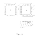
- FIGS. 1A-1D show a single integrated circuit die (shown after singulation for clarity) packaged in accordance with an exemplary embodiment of the present invention.
- FIGS. 2A-2L show a plurality of integrated circuit dice mounted in a substrate in accordance with an exemplary embodiment of the present invention.
- any type of integrated circuit device may be utilized in accordance with specific exemplary embodiments of the present invention described herein.
- the techniques for fabricating various types of integrated circuit devices are known in the art and will not be discussed. Significantly, the production of the integrated circuit devices is unimportant for an appreciation of the present invention. Therefore, only details related to mounting the integrated circuit devices in a substrate will be described.
- an integrated circuit die 101 is fabricated with a plurality of interconnects or contact pads 103 . Although all features described are typically fabricated while the die is still in wafer form, a single die is shown for clarity and ease of understanding. A skilled artisan will recognize that techniques disclosed herein allow all integrated circuit dice on a wafer or from various wafers to be mass aligned, thus resulting in shorter and more efficient overall fabrication times.
- the alignment feature 105 is formed over the integrated circuit die 101 .
- the alignment feature 105 may be, for example, a photoresist layer or another photolithographically definable material.
- the alignment feature 105 is formed by standard photolithography techniques including exposing a photo-definable material such as, for example, photoresist, and developing and etching the material.
- the alignment feature 105 has two alignment edges. Since fabrication of the alignment edges is performed while the integrated circuit die 101 is still in wafer form, alignment of the alignment feature 105 relative to the contact pads 103 is readily achieved.
- Other alignment means may be readily envisioned by a skilled artisan and are within a scope of embodiments described herein. Such other means may include, for example, alignment to features etched or protruding from edges of the alignment feature 105 . Such features are readily achievable by producing the features in a reticle used to expose the photo-definable material. As shown in the exemplary embodiment of FIG. 1A , a corner at the intersection of the two alignment edges has been chamfered. The chamfering helps prevent any misalignment issues which may otherwise arise in later edge alignment stages due to, for example, any excess material formed at the corner thus preventing a 90° intersection of the edges from being formed.
- a windowed alignment mask 107 includes a window 109 .
- the window 109 has two edges arranged to allow precise and accurate positional referencing for the integrated circuit die 101 .
- the integrated circuit die 101 with the alignment feature 105 is flipped and inserted into the windowed alignment mask 107 .
- the alignment feature 105 thus drops into the window 109 .
- the first spacing gaps 111 are shown as a uniform gap between the alignment feature 105 and the windowed alignment mask 107 merely as an illustrational aid.
- windowed alignment mask 107 and the alignment feature 105 are shown having the same thickness, there is no requirement for each element being of the same thickness as long as the alignment feature 105 is able to drop fully into the window 109 such that an uppermost surface of the integrated circuit die 101 (i.e., that surface containing the plurality of contact pads 103 ) is substantially coplanar and in contact with an uppermost portion of the windowed alignment mask 107 .
- the alignment edges of the integrated circuit die 101 are mechanically biased relative to coordinate positions 0, 0 relative to alignment edges on the windowed alignment mask 107 .
- the mechanical biasing may be achieved by, for example, pushing the integrated circuit die 101 with a small tool such as a vacuum pick (although vacuum assistance is not required).
- the mechanical biasing may be achieved by tilting the windowed alignment mask 107 such that gravity allows the integrated circuit die 101 to be positioned correctly.
- the alignment edges of both the integrated circuit die 101 and the windowed alignment mask 107 are in physical contact leaving a set of second spacing gaps 113 on the top and right edges as indicated in the plan view of FIG. 1D .
- the second spacing gaps 113 are consequently larger than the first spacing gaps 111 of FIG. 1C as the mechanical biasing has removed portions of the first spacing gaps on the left and bottom edges. With the mechanical biasing completed, the integrated circuit die 101 is now aligned with respect to the windowed alignment mask 107 .
- Various types of adhesives e.g., an ultraviolet-curable adhesive
- adhesives e.g., an ultraviolet-curable adhesive
- FIGS. 2A-2L describe in more complete detail how the packaging concept applies to a plurality of integrated circuit dice from a single wafer or integrated circuit dice generally (e.g., dice from different wafers or dice containing a variety of circuit types)
- a plurality of integrated circuit dice 201 are shown.
- Each of the plurality of integrated circuit dice 201 has a plurality of interconnects or contact pads 203 and an alignment feature 205 .
- the alignment feature 205 is formed over each of the plurality of integrated circuit dice 201 .
- the alignment feature 205 may be, for example, a photoresist layer or another photolithographically definable material.
- the alignment feature 205 is formed by standard photolithography techniques including exposing a photo-definable material such as, for example, photoresist, developing, and etching the material.
- the alignment feature 205 has two alignment edges. Fabrication of the alignment feature 205 is performed while the integrated circuit die 201 is still in wafer form. Thus, a location of the alignment feature relative to the contact pads 203 is readily achieved since positional accuracy of the alignment features is equal to any other 30 photolithographic fabrication step.
- a windowed alignment mask 207 includes a plurality of windows 209 . Similar to FIG. 1B , each of the plurality of windows 209 has two edges arranged to allow precise and accurate positional referencing for the plurality of integrated circuit dice 201 . The positional reference as shown here is relative to a coordinate of 0, 0. Each of the windows 209 corresponds to a position of each of the plurality of integrated circuit dice 201 in a final packaged form (not shown). Further, each of the plurality of windows 209 is slightly larger than an x-y dimension of a corresponding one of the alignment features 205 on the plurality of integrated circuit dice 201 . The larger size allows easy insertion of the alignment features 205 .
- the windowed alignment mask 207 can be formed from, for example, organic or inorganic materials including glass, silicon, steel epoxy laminates, plastic polymers, and other materials known to one of skill in the art. Fabrication of the windowed alignment mask 207 may be accomplished by appropriate applications of machining, chemical etching, mechanical punching operations, or other techniques. A thickness of the windowed alignment mask 207 is typically equal to or greater than a maximum thickness of the plurality of integrated circuit dice 201 .
- a windowed substrate 211 includes a plurality of windows 213 and a plurality of vias 215 .
- the plurality of vias 215 is only an exemplary embodiment and relates to stacked combinations of semiconductor packages.
- the windowed substrate 211 forms a base onto which the plurality of integrated circuit dice 201 will be placed into and embedded in subsequent operations.
- Each of the plurality of windows 213 corresponds with a particular one of the plurality of integrated circuit dice 201 and is slightly oversized with reference to a specific die to allow easy drop-in of the die. Further, each of the plurality of windows is positionally accurate and precise relative to a 0, 0 coordinate.
- the windowed substrate 211 may be in a substantially round form as shown.
- the windowed substrate 211 has two flatted edges as shown thus emulating a typical wafer form for 150 mm and smaller standard silicon wafers.
- the windowed substrate 211 may be formed with notches to emulate 200 mm, 300 mm or larger wafers.
- the windowed substrate 211 could be square or rectangular as required to suit a particular need.
- each of the plurality of integrated circuit dice 201 is flipped and dropped into a corresponding window on the windowed alignment mask 207 . Due to the slightly oversize nature of the plurality of windows 209 ( FIG. 2B ), a small first set of gaps 217 exists between each of the alignment features 205 and the corresponding window edge.
- the alignment edges of each of the plurality of integrated circuit dice 201 are mechanically biased relative to coordinate 0, 0 (i.e., toward the alignment edges) on the windowed alignment mask 207 as indicated by the arrows.
- the mechanical biasing may be achieved by, for example, pushing each of the plurality of integrated circuit dice 201 with a small tool such as a vacuum pick (although vacuum assistance is not required).
- the mechanical biasing may be achieved by tilting the windowed alignment mask 207 such that gravity allows each of the plurality of integrated circuit dice 201 to be positioned correctly against the alignment edges.
- the alignment edges of the plurality of integrated circuit dice 201 and the windowed alignment mask 207 are in physical contact leaving a set of second spacing gaps 219 on the top and right edges as indicated in the plan view of FIG. 2E .
- the second set of spacing gaps 219 are consequently larger than the first set of spacing gaps 217 of FIG. 2D .
- the windowed substrate 211 is placed over the windowed alignment mask 207 which already contains the aligned plurality of integrated circuit dice 201 .
- X-Y flats on the windowed substrate 211 are aligned with corresponding X-Y edges of the windowed alignment mask 207 as indicated in the plan view of FIG. 2F .
- a third set of gaps 221 now exist between edges of the plurality of integrated circuit dice 201 and inside edges of the plurality of windows 213 ( FIG. 2C ) in the windowed substrate 211 .
- a tack 223 is made in, for example, at least two corners to secure each of the plurality of integrated circuit dice 201 to the windowed substrate 211 . (All four corners are tacked as indicated in the plan view of FIG. 2G .)
- the tack 223 may be a quick curing adhesive (e.g., a UV-curable adhesive) although a person of skill in the art will recognize that various other materials may readily be employed for this purpose as well.
- the tack 223 locks each of the plurality of integrated circuit dice 201 into its position relative to the windows 213 on the windowed substrate 211 .
- the windowed alignment mask 207 may be removed ( FIG. 2H ). Notice the cross-sectional view, Section H-H, in FIG. 2H is inverted with respect to FIG. 2G such that each of the plurality of alignment features 205 are now on top.
- the plurality of alignment features is then removed or stripped ( FIG. 2I ) by, for example, chemical or mechanical means which are well-known in the art.
- the windowed substrate 211 assembly is inverted and placed on a flat surface 225 .
- the flat surface is a high-release (e.g., non-stick) surface such as Teflon®.
- Teflon® is a registered trademark of E.I. du Pont de Nemours and Company and is a synthetic resinous fluorine-containing polymer (polytetrafluoroethylene) commonly found in molding and extruding compositions, fabricated shapes such as sheets, tubes, tape, filaments, and emulsions.
- the third set of gaps 221 ( FIG. 2F ) is substantially filled with a filler material 227 .
- the filler material 227 may be, for example, an epoxy or polymer material and need only be filled sufficiently so as to prevent further movement of plurality of integrated circuit dice 201 .
- the filler material 227 is cured and the windowed substrate 211 assembly is removed from the flat surface 225 ( FIG. 2L ).
- the plurality of integrated circuit dice 201 is precisely and accurately aligned with respect to each other and the plurality of vias 215 or other contact pads (not shown). Any additional levels of interconnect circuitry (not shown) are easily attached to each of the plurality of integrated circuit dice 201 on the windowed substrate 211 assembly.
Abstract
Description
Claims (18)
Priority Applications (1)
| Application Number | Priority Date | Filing Date | Title |
|---|---|---|---|
| US12/784,389 US8044526B2 (en) | 2006-12-27 | 2010-05-20 | Integrated circuit assemblies with alignment features and devices and methods related thereto |
Applications Claiming Priority (2)
| Application Number | Priority Date | Filing Date | Title |
|---|---|---|---|
| US11/616,479 US20080160670A1 (en) | 2006-12-27 | 2006-12-27 | Physical alignment features on integrated circuit devices for accurate die-in-substrate embedding |
| US12/784,389 US8044526B2 (en) | 2006-12-27 | 2010-05-20 | Integrated circuit assemblies with alignment features and devices and methods related thereto |
Related Parent Applications (1)
| Application Number | Title | Priority Date | Filing Date |
|---|---|---|---|
| US11/616,479 Continuation US20080160670A1 (en) | 2006-12-27 | 2006-12-27 | Physical alignment features on integrated circuit devices for accurate die-in-substrate embedding |
Publications (2)
| Publication Number | Publication Date |
|---|---|
| US20100225009A1 US20100225009A1 (en) | 2010-09-09 |
| US8044526B2 true US8044526B2 (en) | 2011-10-25 |
Family
ID=39584564
Family Applications (2)
| Application Number | Title | Priority Date | Filing Date |
|---|---|---|---|
| US11/616,479 Abandoned US20080160670A1 (en) | 2006-12-27 | 2006-12-27 | Physical alignment features on integrated circuit devices for accurate die-in-substrate embedding |
| US12/784,389 Active US8044526B2 (en) | 2006-12-27 | 2010-05-20 | Integrated circuit assemblies with alignment features and devices and methods related thereto |
Family Applications Before (1)
| Application Number | Title | Priority Date | Filing Date |
|---|---|---|---|
| US11/616,479 Abandoned US20080160670A1 (en) | 2006-12-27 | 2006-12-27 | Physical alignment features on integrated circuit devices for accurate die-in-substrate embedding |
Country Status (3)
| Country | Link |
|---|---|
| US (2) | US20080160670A1 (en) |
| TW (1) | TW200841433A (en) |
| WO (1) | WO2008083028A1 (en) |
Cited By (1)
| Publication number | Priority date | Publication date | Assignee | Title |
|---|---|---|---|---|
| US10068881B2 (en) | 2015-12-31 | 2018-09-04 | Samsung Electronics Co., Ltd. | Package-on-package type semiconductor package and method of fabricating the same |
Families Citing this family (2)
| Publication number | Priority date | Publication date | Assignee | Title |
|---|---|---|---|---|
| US20080160670A1 (en) * | 2006-12-27 | 2008-07-03 | Atmel Corporation | Physical alignment features on integrated circuit devices for accurate die-in-substrate embedding |
| US11721636B2 (en) | 2018-04-15 | 2023-08-08 | Hewlett-Packard Development Company, L.P. | Circuit die alignment target |
Citations (11)
| Publication number | Priority date | Publication date | Assignee | Title |
|---|---|---|---|---|
| US5216806A (en) | 1992-09-01 | 1993-06-08 | Atmel Corporation | Method of forming a chip package and package interconnects |
| US6048744A (en) * | 1997-09-15 | 2000-04-11 | Micron Technology, Inc. | Integrated circuit package alignment feature |
| US20010012643A1 (en) | 1998-01-18 | 2001-08-09 | Kabushiki Kaisha Toshiba | Package having very thin semiconductor chip, multichip module assembled by the package, and method for manufacturing the same |
| US6300018B1 (en) * | 1999-09-21 | 2001-10-09 | Tyco Electronics Logistics Ag | Photolithography mask having a subresolution alignment mark window |
| US20010033014A1 (en) | 2000-01-03 | 2001-10-25 | Koh Philip Joseph | High frequency, low cost package for semiconductor devices |
| US6455933B1 (en) * | 1996-03-07 | 2002-09-24 | Micron Technology, Inc. | Underfill of a bumped or raised die utilizing a barrier adjacent to the side wall of flip chip |
| US20020168797A1 (en) | 1994-05-19 | 2002-11-14 | Distefano Thomas H. | Method of manufacturing a plurality of semiconductor packages and the resulting semiconductor package structures |
| US20050032070A1 (en) | 2003-08-05 | 2005-02-10 | Sebastian Raimundo | Polymorphisms in the human gene for CYP2D6 and their use in diagnostic and therapeutic applications |
| US20060032070A1 (en) | 2004-08-11 | 2006-02-16 | Biggs Todd L | Micro tool alignment apparatus and method |
| US7087992B2 (en) | 2002-08-27 | 2006-08-08 | Micron Technology, Inc. | Multichip wafer level packages and computing systems incorporating same |
| US20080160670A1 (en) | 2006-12-27 | 2008-07-03 | Atmel Corporation | Physical alignment features on integrated circuit devices for accurate die-in-substrate embedding |
-
2006
- 2006-12-27 US US11/616,479 patent/US20080160670A1/en not_active Abandoned
-
2007
- 2007-12-14 TW TW096148108A patent/TW200841433A/en unknown
- 2007-12-20 WO PCT/US2007/088321 patent/WO2008083028A1/en active Application Filing
-
2010
- 2010-05-20 US US12/784,389 patent/US8044526B2/en active Active
Patent Citations (14)
| Publication number | Priority date | Publication date | Assignee | Title |
|---|---|---|---|---|
| US5216806A (en) | 1992-09-01 | 1993-06-08 | Atmel Corporation | Method of forming a chip package and package interconnects |
| US20020168797A1 (en) | 1994-05-19 | 2002-11-14 | Distefano Thomas H. | Method of manufacturing a plurality of semiconductor packages and the resulting semiconductor package structures |
| US6455933B1 (en) * | 1996-03-07 | 2002-09-24 | Micron Technology, Inc. | Underfill of a bumped or raised die utilizing a barrier adjacent to the side wall of flip chip |
| US6048744A (en) * | 1997-09-15 | 2000-04-11 | Micron Technology, Inc. | Integrated circuit package alignment feature |
| US20010012643A1 (en) | 1998-01-18 | 2001-08-09 | Kabushiki Kaisha Toshiba | Package having very thin semiconductor chip, multichip module assembled by the package, and method for manufacturing the same |
| US6300018B1 (en) * | 1999-09-21 | 2001-10-09 | Tyco Electronics Logistics Ag | Photolithography mask having a subresolution alignment mark window |
| US20020037598A1 (en) | 2000-01-03 | 2002-03-28 | Sophia Wireless, Inc. | High frequency, low cost package for semiconductor devices |
| US20010033014A1 (en) | 2000-01-03 | 2001-10-25 | Koh Philip Joseph | High frequency, low cost package for semiconductor devices |
| US20030042603A1 (en) | 2000-01-03 | 2003-03-06 | Sophia Wireless, Inc. | High frequency, low cost package for semiconductor devices |
| US7087992B2 (en) | 2002-08-27 | 2006-08-08 | Micron Technology, Inc. | Multichip wafer level packages and computing systems incorporating same |
| US20050032070A1 (en) | 2003-08-05 | 2005-02-10 | Sebastian Raimundo | Polymorphisms in the human gene for CYP2D6 and their use in diagnostic and therapeutic applications |
| US20060032070A1 (en) | 2004-08-11 | 2006-02-16 | Biggs Todd L | Micro tool alignment apparatus and method |
| US20080160670A1 (en) | 2006-12-27 | 2008-07-03 | Atmel Corporation | Physical alignment features on integrated circuit devices for accurate die-in-substrate embedding |
| WO2008083028A1 (en) | 2006-12-27 | 2008-07-10 | Atmel Corporation | Physical alignment features on integrated circuit devices for accurate die-in-substrate embedding |
Non-Patent Citations (8)
| Title |
|---|
| "International Patent Application No. PCT/US07/88321, Written Opinion mailed Apr. 24, 2008", 6 pgs. |
| "U.S. Appl. No. 11/616,479, Final Office Action mailed Jan. 22, 2010", 6 pgs. |
| "U.S. Appl. No. 11/616,479, Interview Summary and Final Office Action mailed Feb. 22, 2010", 8 pgs. |
| "U.S. Appl. No. 11/616,479, Non-Final Office Action mailed May 14, 2009", 9 pgs. |
| "U.S. Appl. No. 11/616,479, Response filed Aug. 14, 2009 to Non-Final Office Action mailed May 14, 2009", 9 pgs. |
| "U.S. Appl. No. 11/616,479, Response filed Oct. 29, 2009 to Restriction Requirement mailed Sep. 29, 2009", 10 pgs. |
| "U.S. Appl. No. 11/616,479, Restriction Requirement mailed Sep. 29, 2009", 4 pgs. |
| International Patent Application No. PCT/US07/88321, Search Report mailed Apr. 24, 2008, 2 pgs. |
Cited By (1)
| Publication number | Priority date | Publication date | Assignee | Title |
|---|---|---|---|---|
| US10068881B2 (en) | 2015-12-31 | 2018-09-04 | Samsung Electronics Co., Ltd. | Package-on-package type semiconductor package and method of fabricating the same |
Also Published As
| Publication number | Publication date |
|---|---|
| US20100225009A1 (en) | 2010-09-09 |
| TW200841433A (en) | 2008-10-16 |
| US20080160670A1 (en) | 2008-07-03 |
| WO2008083028A1 (en) | 2008-07-10 |
Similar Documents
| Publication | Publication Date | Title |
|---|---|---|
| US7943423B2 (en) | Reconfigured wafer alignment | |
| US7518223B2 (en) | Semiconductor devices and semiconductor device assemblies including a nonconfluent spacer layer | |
| US7943422B2 (en) | Wafer level pre-packaged flip chip | |
| US8580612B2 (en) | Chip assembly | |
| US7781867B2 (en) | Method and system for providing an aligned semiconductor assembly | |
| Sharma et al. | Solutions strategies for die shift problem in wafer level compression molding | |
| US10366972B2 (en) | Microelectronics package with self-aligned stacked-die assembly | |
| US10784233B2 (en) | Microelectronics package with self-aligned stacked-die assembly | |
| US8429814B2 (en) | Method of assembling a multi-component electronic package | |
| US20110018115A1 (en) | Pop precursor with interposer for top package bond pad pitch compensation | |
| US20060094240A1 (en) | Neo-wafer device comprised of multiple singulated integrated circuit die | |
| US20060012020A1 (en) | Wafer-level assembly method for semiconductor devices | |
| US8247897B2 (en) | Blank including a composite panel with semiconductor chips and plastic package molding compound and method and mold for producing the same | |
| US8877523B2 (en) | Recovery method for poor yield at integrated circuit die panelization | |
| CN110178209B (en) | Method for manufacturing semiconductor package | |
| US20130285259A1 (en) | Method and system for wafer and strip level batch die attach assembly | |
| US20190109092A1 (en) | Positioning structure having positioning unit | |
| US8044526B2 (en) | Integrated circuit assemblies with alignment features and devices and methods related thereto | |
| TW201611216A (en) | Semiconductor package and its carrier structure and method of manufacture | |
| JP3291289B2 (en) | Electronic component manufacturing method | |
| US20190287944A1 (en) | Asics face to face self assembly | |
| US20230062701A1 (en) | Semiconductor assemblies with system and methods for aligning dies using registration marks | |
| US9177862B2 (en) | Semiconductor stack structure and fabrication method thereof | |
| CN112185823A (en) | Processing one or more carrier bodies and electronic devices by multiple alignment | |
| KR20000069626A (en) | Flip-chip type connection with elastic contacts |
Legal Events
| Date | Code | Title | Description |
|---|---|---|---|
| AS | Assignment |
Owner name: ATMEL CORPORATION, CALIFORNIA Free format text: ASSIGNMENT OF ASSIGNORS INTEREST;ASSIGNOR:LAM, KEN;REEL/FRAME:026114/0166 Effective date: 20061226 |
|
| STCF | Information on status: patent grant |
Free format text: PATENTED CASE |
|
| CC | Certificate of correction | ||
| AS | Assignment |
Owner name: MORGAN STANLEY SENIOR FUNDING, INC. AS ADMINISTRATIVE AGENT, NEW YORK Free format text: PATENT SECURITY AGREEMENT;ASSIGNOR:ATMEL CORPORATION;REEL/FRAME:031912/0173 Effective date: 20131206 Owner name: MORGAN STANLEY SENIOR FUNDING, INC. AS ADMINISTRAT Free format text: PATENT SECURITY AGREEMENT;ASSIGNOR:ATMEL CORPORATION;REEL/FRAME:031912/0173 Effective date: 20131206 |
|
| FPAY | Fee payment |
Year of fee payment: 4 |
|
| AS | Assignment |
Owner name: ATMEL CORPORATION, CALIFORNIA Free format text: TERMINATION AND RELEASE OF SECURITY INTEREST IN PATENT COLLATERAL;ASSIGNOR:MORGAN STANLEY SENIOR FUNDING, INC.;REEL/FRAME:038376/0001 Effective date: 20160404 |
|
| AS | Assignment |
Owner name: JPMORGAN CHASE BANK, N.A., AS ADMINISTRATIVE AGENT, ILLINOIS Free format text: SECURITY INTEREST;ASSIGNOR:ATMEL CORPORATION;REEL/FRAME:041715/0747 Effective date: 20170208 Owner name: JPMORGAN CHASE BANK, N.A., AS ADMINISTRATIVE AGENT Free format text: SECURITY INTEREST;ASSIGNOR:ATMEL CORPORATION;REEL/FRAME:041715/0747 Effective date: 20170208 |
|
| AS | Assignment |
Owner name: JPMORGAN CHASE BANK, N.A., AS ADMINISTRATIVE AGENT, ILLINOIS Free format text: SECURITY INTEREST;ASSIGNORS:MICROCHIP TECHNOLOGY INCORPORATED;SILICON STORAGE TECHNOLOGY, INC.;ATMEL CORPORATION;AND OTHERS;REEL/FRAME:046426/0001 Effective date: 20180529 Owner name: JPMORGAN CHASE BANK, N.A., AS ADMINISTRATIVE AGENT Free format text: SECURITY INTEREST;ASSIGNORS:MICROCHIP TECHNOLOGY INCORPORATED;SILICON STORAGE TECHNOLOGY, INC.;ATMEL CORPORATION;AND OTHERS;REEL/FRAME:046426/0001 Effective date: 20180529 |
|
| AS | Assignment |
Owner name: WELLS FARGO BANK, NATIONAL ASSOCIATION, AS NOTES COLLATERAL AGENT, CALIFORNIA Free format text: SECURITY INTEREST;ASSIGNORS:MICROCHIP TECHNOLOGY INCORPORATED;SILICON STORAGE TECHNOLOGY, INC.;ATMEL CORPORATION;AND OTHERS;REEL/FRAME:047103/0206 Effective date: 20180914 Owner name: WELLS FARGO BANK, NATIONAL ASSOCIATION, AS NOTES C Free format text: SECURITY INTEREST;ASSIGNORS:MICROCHIP TECHNOLOGY INCORPORATED;SILICON STORAGE TECHNOLOGY, INC.;ATMEL CORPORATION;AND OTHERS;REEL/FRAME:047103/0206 Effective date: 20180914 |
|
| MAFP | Maintenance fee payment |
Free format text: PAYMENT OF MAINTENANCE FEE, 8TH YEAR, LARGE ENTITY (ORIGINAL EVENT CODE: M1552); ENTITY STATUS OF PATENT OWNER: LARGE ENTITY Year of fee payment: 8 |
|
| AS | Assignment |
Owner name: JPMORGAN CHASE BANK, N.A., AS ADMINISTRATIVE AGENT, DELAWARE Free format text: SECURITY INTEREST;ASSIGNORS:MICROCHIP TECHNOLOGY INC.;SILICON STORAGE TECHNOLOGY, INC.;ATMEL CORPORATION;AND OTHERS;REEL/FRAME:053311/0305 Effective date: 20200327 |
|
| AS | Assignment |
Owner name: MICROSEMI CORPORATION, CALIFORNIA Free format text: RELEASE BY SECURED PARTY;ASSIGNOR:JPMORGAN CHASE BANK, N.A, AS ADMINISTRATIVE AGENT;REEL/FRAME:053466/0011 Effective date: 20200529 Owner name: MICROSEMI STORAGE SOLUTIONS, INC., ARIZONA Free format text: RELEASE BY SECURED PARTY;ASSIGNOR:JPMORGAN CHASE BANK, N.A, AS ADMINISTRATIVE AGENT;REEL/FRAME:053466/0011 Effective date: 20200529 Owner name: MICROCHIP TECHNOLOGY INC., ARIZONA Free format text: RELEASE BY SECURED PARTY;ASSIGNOR:JPMORGAN CHASE BANK, N.A, AS ADMINISTRATIVE AGENT;REEL/FRAME:053466/0011 Effective date: 20200529 Owner name: SILICON STORAGE TECHNOLOGY, INC., ARIZONA Free format text: RELEASE BY SECURED PARTY;ASSIGNOR:JPMORGAN CHASE BANK, N.A, AS ADMINISTRATIVE AGENT;REEL/FRAME:053466/0011 Effective date: 20200529 Owner name: ATMEL CORPORATION, ARIZONA Free format text: RELEASE BY SECURED PARTY;ASSIGNOR:JPMORGAN CHASE BANK, N.A, AS ADMINISTRATIVE AGENT;REEL/FRAME:053466/0011 Effective date: 20200529 |
|
| AS | Assignment |
Owner name: WELLS FARGO BANK, NATIONAL ASSOCIATION, MINNESOTA Free format text: SECURITY INTEREST;ASSIGNORS:MICROCHIP TECHNOLOGY INC.;SILICON STORAGE TECHNOLOGY, INC.;ATMEL CORPORATION;AND OTHERS;REEL/FRAME:053468/0705 Effective date: 20200529 |
|
| AS | Assignment |
Owner name: WELLS FARGO BANK, NATIONAL ASSOCIATION, AS COLLATERAL AGENT, MINNESOTA Free format text: SECURITY INTEREST;ASSIGNORS:MICROCHIP TECHNOLOGY INCORPORATED;SILICON STORAGE TECHNOLOGY, INC.;ATMEL CORPORATION;AND OTHERS;REEL/FRAME:055671/0612 Effective date: 20201217 |
|
| AS | Assignment |
Owner name: WELLS FARGO BANK, NATIONAL ASSOCIATION, AS NOTES COLLATERAL AGENT, MINNESOTA Free format text: SECURITY INTEREST;ASSIGNORS:MICROCHIP TECHNOLOGY INCORPORATED;SILICON STORAGE TECHNOLOGY, INC.;ATMEL CORPORATION;AND OTHERS;REEL/FRAME:057935/0474 Effective date: 20210528 |
|
| AS | Assignment |
Owner name: MICROSEMI STORAGE SOLUTIONS, INC., ARIZONA Free format text: RELEASE BY SECURED PARTY;ASSIGNOR:JPMORGAN CHASE BANK, N.A., AS ADMINISTRATIVE AGENT;REEL/FRAME:059333/0222 Effective date: 20220218 Owner name: MICROSEMI CORPORATION, ARIZONA Free format text: RELEASE BY SECURED PARTY;ASSIGNOR:JPMORGAN CHASE BANK, N.A., AS ADMINISTRATIVE AGENT;REEL/FRAME:059333/0222 Effective date: 20220218 Owner name: ATMEL CORPORATION, ARIZONA Free format text: RELEASE BY SECURED PARTY;ASSIGNOR:JPMORGAN CHASE BANK, N.A., AS ADMINISTRATIVE AGENT;REEL/FRAME:059333/0222 Effective date: 20220218 Owner name: SILICON STORAGE TECHNOLOGY, INC., ARIZONA Free format text: RELEASE BY SECURED PARTY;ASSIGNOR:JPMORGAN CHASE BANK, N.A., AS ADMINISTRATIVE AGENT;REEL/FRAME:059333/0222 Effective date: 20220218 Owner name: MICROCHIP TECHNOLOGY INCORPORATED, ARIZONA Free format text: RELEASE BY SECURED PARTY;ASSIGNOR:JPMORGAN CHASE BANK, N.A., AS ADMINISTRATIVE AGENT;REEL/FRAME:059333/0222 Effective date: 20220218 |
|
| AS | Assignment |
Owner name: ATMEL CORPORATION, ARIZONA Free format text: RELEASE BY SECURED PARTY;ASSIGNOR:JPMORGAN CHASE BANK, N.A., AS ADMINISTRATIVE AGENT;REEL/FRAME:059262/0105 Effective date: 20220218 |
|
| AS | Assignment |
Owner name: MICROSEMI STORAGE SOLUTIONS, INC., ARIZONA Free format text: RELEASE BY SECURED PARTY;ASSIGNOR:WELLS FARGO BANK, NATIONAL ASSOCIATION, AS NOTES COLLATERAL AGENT;REEL/FRAME:059358/0001 Effective date: 20220228 Owner name: MICROSEMI CORPORATION, ARIZONA Free format text: RELEASE BY SECURED PARTY;ASSIGNOR:WELLS FARGO BANK, NATIONAL ASSOCIATION, AS NOTES COLLATERAL AGENT;REEL/FRAME:059358/0001 Effective date: 20220228 Owner name: ATMEL CORPORATION, ARIZONA Free format text: RELEASE BY SECURED PARTY;ASSIGNOR:WELLS FARGO BANK, NATIONAL ASSOCIATION, AS NOTES COLLATERAL AGENT;REEL/FRAME:059358/0001 Effective date: 20220228 Owner name: SILICON STORAGE TECHNOLOGY, INC., ARIZONA Free format text: RELEASE BY SECURED PARTY;ASSIGNOR:WELLS FARGO BANK, NATIONAL ASSOCIATION, AS NOTES COLLATERAL AGENT;REEL/FRAME:059358/0001 Effective date: 20220228 Owner name: MICROCHIP TECHNOLOGY INCORPORATED, ARIZONA Free format text: RELEASE BY SECURED PARTY;ASSIGNOR:WELLS FARGO BANK, NATIONAL ASSOCIATION, AS NOTES COLLATERAL AGENT;REEL/FRAME:059358/0001 Effective date: 20220228 |
|
| AS | Assignment |
Owner name: MICROSEMI STORAGE SOLUTIONS, INC., ARIZONA Free format text: RELEASE BY SECURED PARTY;ASSIGNOR:WELLS FARGO BANK, NATIONAL ASSOCIATION, AS NOTES COLLATERAL AGENT;REEL/FRAME:059863/0400 Effective date: 20220228 Owner name: MICROSEMI CORPORATION, ARIZONA Free format text: RELEASE BY SECURED PARTY;ASSIGNOR:WELLS FARGO BANK, NATIONAL ASSOCIATION, AS NOTES COLLATERAL AGENT;REEL/FRAME:059863/0400 Effective date: 20220228 Owner name: ATMEL CORPORATION, ARIZONA Free format text: RELEASE BY SECURED PARTY;ASSIGNOR:WELLS FARGO BANK, NATIONAL ASSOCIATION, AS NOTES COLLATERAL AGENT;REEL/FRAME:059863/0400 Effective date: 20220228 Owner name: SILICON STORAGE TECHNOLOGY, INC., ARIZONA Free format text: RELEASE BY SECURED PARTY;ASSIGNOR:WELLS FARGO BANK, NATIONAL ASSOCIATION, AS NOTES COLLATERAL AGENT;REEL/FRAME:059863/0400 Effective date: 20220228 Owner name: MICROCHIP TECHNOLOGY INCORPORATED, ARIZONA Free format text: RELEASE BY SECURED PARTY;ASSIGNOR:WELLS FARGO BANK, NATIONAL ASSOCIATION, AS NOTES COLLATERAL AGENT;REEL/FRAME:059863/0400 Effective date: 20220228 |
|
| AS | Assignment |
Owner name: MICROSEMI STORAGE SOLUTIONS, INC., ARIZONA Free format text: RELEASE BY SECURED PARTY;ASSIGNOR:WELLS FARGO BANK, NATIONAL ASSOCIATION, AS NOTES COLLATERAL AGENT;REEL/FRAME:059363/0001 Effective date: 20220228 Owner name: MICROSEMI CORPORATION, ARIZONA Free format text: RELEASE BY SECURED PARTY;ASSIGNOR:WELLS FARGO BANK, NATIONAL ASSOCIATION, AS NOTES COLLATERAL AGENT;REEL/FRAME:059363/0001 Effective date: 20220228 Owner name: ATMEL CORPORATION, ARIZONA Free format text: RELEASE BY SECURED PARTY;ASSIGNOR:WELLS FARGO BANK, NATIONAL ASSOCIATION, AS NOTES COLLATERAL AGENT;REEL/FRAME:059363/0001 Effective date: 20220228 Owner name: SILICON STORAGE TECHNOLOGY, INC., ARIZONA Free format text: RELEASE BY SECURED PARTY;ASSIGNOR:WELLS FARGO BANK, NATIONAL ASSOCIATION, AS NOTES COLLATERAL AGENT;REEL/FRAME:059363/0001 Effective date: 20220228 Owner name: MICROCHIP TECHNOLOGY INCORPORATED, ARIZONA Free format text: RELEASE BY SECURED PARTY;ASSIGNOR:WELLS FARGO BANK, NATIONAL ASSOCIATION, AS NOTES COLLATERAL AGENT;REEL/FRAME:059363/0001 Effective date: 20220228 |
|
| AS | Assignment |
Owner name: MICROSEMI STORAGE SOLUTIONS, INC., ARIZONA Free format text: RELEASE BY SECURED PARTY;ASSIGNOR:WELLS FARGO BANK, NATIONAL ASSOCIATION, AS NOTES COLLATERAL AGENT;REEL/FRAME:060894/0437 Effective date: 20220228 Owner name: MICROSEMI CORPORATION, ARIZONA Free format text: RELEASE BY SECURED PARTY;ASSIGNOR:WELLS FARGO BANK, NATIONAL ASSOCIATION, AS NOTES COLLATERAL AGENT;REEL/FRAME:060894/0437 Effective date: 20220228 Owner name: ATMEL CORPORATION, ARIZONA Free format text: RELEASE BY SECURED PARTY;ASSIGNOR:WELLS FARGO BANK, NATIONAL ASSOCIATION, AS NOTES COLLATERAL AGENT;REEL/FRAME:060894/0437 Effective date: 20220228 Owner name: SILICON STORAGE TECHNOLOGY, INC., ARIZONA Free format text: RELEASE BY SECURED PARTY;ASSIGNOR:WELLS FARGO BANK, NATIONAL ASSOCIATION, AS NOTES COLLATERAL AGENT;REEL/FRAME:060894/0437 Effective date: 20220228 Owner name: MICROCHIP TECHNOLOGY INCORPORATED, ARIZONA Free format text: RELEASE BY SECURED PARTY;ASSIGNOR:WELLS FARGO BANK, NATIONAL ASSOCIATION, AS NOTES COLLATERAL AGENT;REEL/FRAME:060894/0437 Effective date: 20220228 |
|
| MAFP | Maintenance fee payment |
Free format text: PAYMENT OF MAINTENANCE FEE, 12TH YEAR, LARGE ENTITY (ORIGINAL EVENT CODE: M1553); ENTITY STATUS OF PATENT OWNER: LARGE ENTITY Year of fee payment: 12 |