US8044473B2 - Light sensor - Google Patents
Light sensor Download PDFInfo
- Publication number
- US8044473B2 US8044473B2 US11/972,056 US97205608A US8044473B2 US 8044473 B2 US8044473 B2 US 8044473B2 US 97205608 A US97205608 A US 97205608A US 8044473 B2 US8044473 B2 US 8044473B2
- Authority
- US
- United States
- Prior art keywords
- ion doping
- area
- sensing region
- light
- doping area
- Prior art date
- Legal status (The legal status is an assumption and is not a legal conclusion. Google has not performed a legal analysis and makes no representation as to the accuracy of the status listed.)
- Active, expires
Links
Images


Classifications
-
- H—ELECTRICITY
- H10—SEMICONDUCTOR DEVICES; ELECTRIC SOLID-STATE DEVICES NOT OTHERWISE PROVIDED FOR
- H10F—INORGANIC SEMICONDUCTOR DEVICES SENSITIVE TO INFRARED RADIATION, LIGHT, ELECTROMAGNETIC RADIATION OF SHORTER WAVELENGTH OR CORPUSCULAR RADIATION
- H10F30/00—Individual radiation-sensitive semiconductor devices in which radiation controls the flow of current through the devices, e.g. photodetectors
- H10F30/20—Individual radiation-sensitive semiconductor devices in which radiation controls the flow of current through the devices, e.g. photodetectors the devices having potential barriers, e.g. phototransistors
- H10F30/21—Individual radiation-sensitive semiconductor devices in which radiation controls the flow of current through the devices, e.g. photodetectors the devices having potential barriers, e.g. phototransistors the devices being sensitive to infrared, visible or ultraviolet radiation
- H10F30/28—Individual radiation-sensitive semiconductor devices in which radiation controls the flow of current through the devices, e.g. photodetectors the devices having potential barriers, e.g. phototransistors the devices being sensitive to infrared, visible or ultraviolet radiation the devices being characterised by field-effect operation, e.g. junction field-effect phototransistors
- H10F30/282—Insulated-gate field-effect transistors [IGFET], e.g. MISFET [metal-insulator-semiconductor field-effect transistor] phototransistors
Definitions
- the present invention relates to a light sensor and its manufacture method, and more particularly, to a light sensor and its manufacture method without using a CMOS process.
- LCDs liquid crystal displays
- PDA personal digital assistances
- desktop computer screens desktop computer screens
- notebook computer screens notebook computer screens
- touch-control LCDs with an LCD touch panel to allow direct touch by the users have become the trend in the LCD market.
- Conventional resistor type or capacitor type LCD touch panels which are configured by disposing additional resistors or capacitors on the panels, determine the coordinate positions of touch-points by detecting the voltage variation at the touch positions.
- resistors and capacitors are directly disposed on the panels, light transmittance through the LCD panel will be decreased and the overall thickness of the LCD panel will be increased.
- Another type of LCD touch panel, called an optical touch panel is configured by disposing a large amount of light sources and corresponding optical detecting elements around an LCD panel.
- the coordinate position of a touch-point is determined when determining the position of an optical detecting element has failed to receive light rays from a corresponding light source. Although this design would not decrease the overall light transmittance through the panel, the product size is significantly increased. Accordingly, a touch-control LCD with detecting elements incorporated into a touch panel thereof is desirable to decrease the weight and volume of the LCD and thus meets the compact demand of the LCD market.
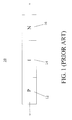
- the light sensor diode 10 is a P-I-N diode which contains a P-type area 12 doped with P-type dopants, an intrinsic layer 14 and an N-type area 16 doped with N-type dopants.
- the function of the intrinsic layer 14 is to increment a thickness of PN depletion region, so as to increase possibility of attracting photons and to reduce junction capacitor.
- the light sensor diode 10 induces electrical potential or photocurrent in accordance with incident light.
- the intrinsic layer 14 is manufactured by poly-Si process.
- the intrinsic layer 14 manufactured by poly-Si has a lower sensitivity in sensing visible light. As a result, it is desirable to develop a new light sensor.
- the present invention provides a light sensor capable of reducing manufacture processes and having better light sensitivity.
- a light sensor comprises an intrinsic layer comprising a first light sensing region and a channel, a first ion doping area disposed at a first side of the intrinsic layer, a second ion doping area disposed at a second side of the intrinsic layer opposite to the first side, an oxide insulating layer disposed on the intrinsic layer, and a gate metal disposed on the oxide insulating layer.
- the first light sensing region adjacent to the first ion doping area is used for generating electron-hole pairs in response to luminance of incident light;
- a method of manufacturing a light sensor comprises the steps of: forming a poly crystalline silicon thin film; ion-implanting the poly crystalline silicon thin film by using a first mask to form a first ion doping area and a second ion doping area; depositing an oxide insulating film on the poly crystalline silicon thin film; depositing a metal film on the oxide insulating film; and etching the oxide insulating film and the metal film by using a second mask to form an oxide insulating layer and a gate metal, so that areas of the oxide insulating layer and the gate metal are smaller than that of the poly crystalline silicon thin film without ion-implanting.
- FIG. 1 shows a conventional light sensor.
- FIG. 2 depicts a light sensor according to a first embodiment of the present invention.
- FIG. 3 illustrates a schematic diagram of photocurrent generated in the light sensor.
- FIG. 4 is a characteristic diagram showing a relationship between photocurrent Id and voltage Vg applied on the gate metal, when a various amount light incident to the light sensing region.
- FIG. 5 is a characteristic diagram showing a ratio between the photocurrent and dark current with a width of a first sensing region being 2 ⁇ m, under various luminance and voltage Vg applied on the gate metal.
- FIG. 6 shows a light sensor according to a second embodiment of the present invention.
- FIG. 7 illustrates a flowchart of a method for manufacturing the light sensor shown in FIG. 2 .
- FIG. 2 depicts a light sensor according to a first embodiment of the present invention.
- the light sensor 30 comprises a first ion doping area 321 , a second ion doping area 322 , an intrinsic layer 34 , an oxide insulating layer 38 , and a metal film 36 which is a gate.
- the intrinsic layer 34 is positioned between the second ion doping area 322 and the first ion doping area 321 .
- Doping ions in the first ion doping area 321 e.g. P-type ions or N-type ions, are similar to that in the second doping area 322 .
- both ion densities of the first ion doping area 321 and the second ion doping area 322 substantially equals to 10 18 atoms/cm 3 .
- the oxide insulating layer 38 is positioned on the intrinsic layer 34 , and the metal film gate 36 overlaps the oxide insulating layer 38 .
- the intrinsic layer 34 further comprises a first light sensing region 341 adjacent to the first ion doping area 321 , a second light sensing region 342 adjacent to the second ion doping area 322 , and a channel 343 .
- the intrinsic layer 34 , the first ion doping area 321 , and the second ion doping area 322 are made of poly crystalline silicon.
- ion density of the poly crystalline silicon is substantially in a range between 10 11 to 10 14 atoms/cm 3 .
- an area of the metal film gate 36 and the oxide insulating layer 38 overlapping the intrinsic layer 34 is smaller than areas of the channel 343 and the first light sensing region 341 .
- an area of the metal film gate 36 and oxide insulating layer 38 overlapping the first light sensing region 341 is smaller than an area of the first light sensing region 341 which is not overlapped by the metal film gate 36 and oxide insulating layer 38 .
- an area of the metal film gate 36 and oxide insulating layer 38 overlapping the second light sensing region 342 is smaller than an area of the second light sensing region 342 which is not overlapped by the metal film gate 36 and oxide insulating layer 38 .
- FIG. 3 illustrates a schematic diagram of photocurrent generated in the light sensor.
- FIG. 4 is a characteristic diagram showing a relationship between photocurrent Id and voltage Vg applied on the gate metal, when the light sensing region 341 is illuminated with various luminances.
- FIG. 5 is a characteristic diagram showing a ratio between the photocurrent and dark current with a width of a first sensing region 341 being 2 ⁇ m, under various luminance and voltage Vg applied on the gate metal. Electron-hole pairs are induced by incident light to the first light sensing region 341 .
- the sensed photocurrent Id rapidly increments as a increase in luminance of light. For example, when light of 10 Lux is incident to the first light sensing region 341 , the photocurrent Id is as approximately 2 times as dark current in indicative of generated current with no incident light. When light of 1700 Lux is incident to the first light sensing region 341 , the photocurrent Id is as approximately 160 times as dark current.
- the sensed photocurrent Id slightly increments as a increase in luminance of light. For example, when light of 10 Lux is incident to the first light sensing region 341 , the photocurrent Id is almost the same as dark current. When light of 1700 Lux is incident to the first light sensing region 341 , the photocurrent Id is as 2.47 times as dark current. As a result, the light sensor of the present invention has well light sensitivity.
- the light sensor 50 has only one light sensing region 341 close to the first ion doping area 321 .(second ion doping area 322 ).
- FIG. 7 illustrates a flowchart of a method for manufacturing the light sensor shown in FIG. 2 .
- the method comprises the steps as follows:
- the light sensor according to the present invention is formed by utilizing only one ion-implanting step (Step 704 ) without using complex CMOS processes, thereby reducing cost for CMOS processes and keeping well light sensitivity.
Landscapes
- Light Receiving Elements (AREA)
Abstract
Description
- Step 700: Depositing an amorphous silicon thin film.
- Step 702: Recrystallizing the amorphous silicon thin film as a poly crystalline silicon thin film.
- Step 704: Ion-implanting the poly crystalline silicon thin film by using a first mask to form a first ion doping area and a second ion doping area. It should be noted that the implanted ions in the first ion doping area and the second ion doping area are P-type (or N-type) ions.
- Step 706: Depositing an oxide insulating film on the poly crystalline silicon thin film.
- Step 708: Depositing a metal film on the oxide insulating film.
- Step 710: Etching the oxide insulating film and the metal film by using a second mask to form an oxide insulating layer and a metal film gate, so that areas of the oxide insulating layer and the metal film gate are smaller than that of the poly crystalline silicon thin film without ion-implanting.
Claims (13)
Applications Claiming Priority (3)
| Application Number | Priority Date | Filing Date | Title |
|---|---|---|---|
| TW096136219 | 2007-09-28 | ||
| TW096136219A TWI348770B (en) | 2007-09-28 | 2007-09-28 | Light sensor |
| TW96136219A | 2007-09-28 |
Publications (2)
| Publication Number | Publication Date |
|---|---|
| US20090085036A1 US20090085036A1 (en) | 2009-04-02 |
| US8044473B2 true US8044473B2 (en) | 2011-10-25 |
Family
ID=40507144
Family Applications (1)
| Application Number | Title | Priority Date | Filing Date |
|---|---|---|---|
| US11/972,056 Active 2029-04-27 US8044473B2 (en) | 2007-09-28 | 2008-01-10 | Light sensor |
Country Status (2)
| Country | Link |
|---|---|
| US (1) | US8044473B2 (en) |
| TW (1) | TWI348770B (en) |
Families Citing this family (1)
| Publication number | Priority date | Publication date | Assignee | Title |
|---|---|---|---|---|
| US9812591B2 (en) * | 2015-06-22 | 2017-11-07 | The Research Foundation For The State University Of New York | Self-balancing position sensitive detector |
Citations (6)
| Publication number | Priority date | Publication date | Assignee | Title |
|---|---|---|---|---|
| US5027177A (en) * | 1989-07-24 | 1991-06-25 | Hughes Aircraft Company | Floating base lateral bipolar phototransistor with field effect gate voltage control |
| US5488000A (en) | 1993-06-22 | 1996-01-30 | Semiconductor Energy Laboratory Co., Ltd. | Method of fabricating a thin film transistor using a nickel silicide layer to promote crystallization of the amorphous silicon layer |
| US20040043676A1 (en) | 2002-08-30 | 2004-03-04 | Toshiba Matsushita Display Technology Co., Ltd. | Suppression of leakage current in image acquisition |
| US20050156261A1 (en) | 2003-12-24 | 2005-07-21 | Sanyo Electric Co., Ltd. | Optical sensor and display |
| US20050285167A1 (en) | 2003-06-16 | 2005-12-29 | Chandra Mouli | Photodiode with self-aligned implants for high quantum efficiency and method of formation |
| US20060138421A1 (en) * | 2004-12-28 | 2006-06-29 | Norio Tada | Photoelectric conversion element and display device including the same |
-
2007
- 2007-09-28 TW TW096136219A patent/TWI348770B/en active
-
2008
- 2008-01-10 US US11/972,056 patent/US8044473B2/en active Active
Patent Citations (6)
| Publication number | Priority date | Publication date | Assignee | Title |
|---|---|---|---|---|
| US5027177A (en) * | 1989-07-24 | 1991-06-25 | Hughes Aircraft Company | Floating base lateral bipolar phototransistor with field effect gate voltage control |
| US5488000A (en) | 1993-06-22 | 1996-01-30 | Semiconductor Energy Laboratory Co., Ltd. | Method of fabricating a thin film transistor using a nickel silicide layer to promote crystallization of the amorphous silicon layer |
| US20040043676A1 (en) | 2002-08-30 | 2004-03-04 | Toshiba Matsushita Display Technology Co., Ltd. | Suppression of leakage current in image acquisition |
| US20050285167A1 (en) | 2003-06-16 | 2005-12-29 | Chandra Mouli | Photodiode with self-aligned implants for high quantum efficiency and method of formation |
| US20050156261A1 (en) | 2003-12-24 | 2005-07-21 | Sanyo Electric Co., Ltd. | Optical sensor and display |
| US20060138421A1 (en) * | 2004-12-28 | 2006-06-29 | Norio Tada | Photoelectric conversion element and display device including the same |
Also Published As
| Publication number | Publication date |
|---|---|
| US20090085036A1 (en) | 2009-04-02 |
| TWI348770B (en) | 2011-09-11 |
| TW200915593A (en) | 2009-04-01 |
Similar Documents
| Publication | Publication Date | Title |
|---|---|---|
| KR100659620B1 (en) | Touch panel | |
| US20100308345A1 (en) | Light sensing system | |
| US9147706B2 (en) | Semiconductor device having sensor circuit having amplifier circuit | |
| TWI424558B (en) | Display | |
| CN102007607A (en) | Photosensitive structure and apparatus including such a structure | |
| JPWO2006129428A1 (en) | Photodiode and display device | |
| US8502772B2 (en) | Driving method of input/output device | |
| US11349044B2 (en) | Photodetection film, photodetection sensor and photodetection display apparatus including the photodetection film, and method of making the photodetection film | |
| EP2527913A1 (en) | Display device | |
| US8044473B2 (en) | Light sensor | |
| US8063464B2 (en) | Photo detector and method for forming thereof | |
| WO2020186425A1 (en) | Photosensor, display apparatus, and method of fabricating photosensor | |
| US6943070B2 (en) | Complementary metal oxide semiconductor image sensor and method of manufacturing the same | |
| US20090159893A1 (en) | Light-receiving element and display device | |
| TWI409533B (en) | Touch display panel | |
| US8426937B2 (en) | Light sensor and display | |
| WO2010032632A1 (en) | Optical sensing element, optical sensing device, and display device with optical sensor function | |
| Lee et al. | In-cell adaptive touch technology for a flexible e-paper display | |
| CN100536174C (en) | Photoelectric sensing element | |
| CN101471391B (en) | Light-receiving element and display device | |
| US20130207190A1 (en) | Semiconductor device, and method for producing same | |
| JP2009158553A (en) | Light receiving element and display device | |
| US8222645B2 (en) | Display device | |
| KR20170123931A (en) | Method for operating transition metal molybdenum disulfide based photosensor | |
| JP2006330322A (en) | Liquid crystal display device |
Legal Events
| Date | Code | Title | Description |
|---|---|---|---|
| AS | Assignment |
Owner name: AU OPTRONICS CORP., TAIWAN Free format text: ASSIGNMENT OF ASSIGNORS INTEREST;ASSIGNORS:CHEN, CHI-WEN;CHANG, MENG-HSIANG;REEL/FRAME:020347/0269;SIGNING DATES FROM 20071114 TO 20071214 Owner name: AU OPTRONICS CORP., TAIWAN Free format text: ASSIGNMENT OF ASSIGNORS INTEREST;ASSIGNORS:CHEN, CHI-WEN;CHANG, MENG-HSIANG;SIGNING DATES FROM 20071114 TO 20071214;REEL/FRAME:020347/0269 |
|
| STCF | Information on status: patent grant |
Free format text: PATENTED CASE |
|
| FPAY | Fee payment |
Year of fee payment: 4 |
|
| MAFP | Maintenance fee payment |
Free format text: PAYMENT OF MAINTENANCE FEE, 8TH YEAR, LARGE ENTITY (ORIGINAL EVENT CODE: M1552); ENTITY STATUS OF PATENT OWNER: LARGE ENTITY Year of fee payment: 8 |
|
| MAFP | Maintenance fee payment |
Free format text: PAYMENT OF MAINTENANCE FEE, 12TH YEAR, LARGE ENTITY (ORIGINAL EVENT CODE: M1553); ENTITY STATUS OF PATENT OWNER: LARGE ENTITY Year of fee payment: 12 |