US8041865B2 - Bus termination system and method - Google Patents
Bus termination system and method Download PDFInfo
- Publication number
- US8041865B2 US8041865B2 US12/185,472 US18547208A US8041865B2 US 8041865 B2 US8041865 B2 US 8041865B2 US 18547208 A US18547208 A US 18547208A US 8041865 B2 US8041865 B2 US 8041865B2
- Authority
- US
- United States
- Prior art keywords
- bus
- resistance
- memory
- data
- coupled
- Prior art date
- Legal status (The legal status is an assumption and is not a legal conclusion. Google has not performed a legal analysis and makes no representation as to the accuracy of the status listed.)
- Active, expires
Links
Images


Classifications
-
- G—PHYSICS
- G06—COMPUTING OR CALCULATING; COUNTING
- G06F—ELECTRIC DIGITAL DATA PROCESSING
- G06F13/00—Interconnection of, or transfer of information or other signals between, memories, input/output devices or central processing units
- G06F13/38—Information transfer, e.g. on bus
- G06F13/40—Bus structure
- G06F13/4063—Device-to-bus coupling
- G06F13/4068—Electrical coupling
- G06F13/4086—Bus impedance matching, e.g. termination
Definitions
- This invention relates generally to electronics and, in particular embodiments, to a bus termination system and method.
- RAM devices are used for integrated circuits in a variety of electrical and electronic applications, such as computers, cellular telephones, radios, and televisions.
- One particular type of semiconductor device is a semiconductor storage device, such as a random access memory (RAM) device.
- RAM devices include many storage cells arranged in a two-dimensional array with two sets of select lines, wordlines and bitlines. An individual storage cell is selected by activating its wordline and its bitline. RAM devices are considered “random access” because any memory cell in an array can be accessed directly if the row and column that intersect at that cell are known.
- DRAM dynamic RAM
- SDRAM synchronous DRAM
- Synchronous dynamic random access memory often takes advantage of the burst mode concept to greatly improve performance by staying on the row containing the requested bit and moving rapidly through the columns.
- DDR double data rate
- the termination resistors on the circuit board reduce some reflections on the signal lines, they are unable to prevent reflections resulting from the stub lines that connect to the chips.
- a signal propagating from the controller to the components encounters an impedance discontinuity at each stub leading to the chips on the module. As a result, a reflection will be generated at each stub independent of the termination setting. It is desired, however, to minimize the impact of these reflections.
- a system in one embodiment, includes a number of integrated circuit chips coupled to a bus. Each of the integrated circuit chips has an input/output node coupled to the bus, the input/output node having a programmable on-die termination resistor. When the input/output node of one of the integrated circuit chips is accessed via the bus, the programmable on-die termination resistor of each of the integrated circuit chips can be independently set to a termination resistance. The termination resistance is determined by a transaction type and which of the plurality memory devices is being accessed.
- FIG. 1 is a block diagram of a conventional memory system
- FIG. 2 is a block diagram of an embodiment memory system of the present invention
- FIG. 3 is a block diagram of an embodiment memory device of the present invention.
- FIG. 4 is block diagram showing a first embodiment of the invention
- FIG. 5 is a block diagram showing one specific implementation
- FIG. 6 is a block diagram of an embodiment memory device of the present invention.
- FIG. 7 is a block diagram of an embodiment memory device of the present invention.
- FIG. 8 is a block diagram of a computing system that can utilize aspects of the present invention.
- the present invention will be described with respect to preferred embodiments in a specific context, namely a dynamic random access memory module.
- the invention may also be applied, however, to other electronic systems that include more than one chip coupled to a bus.
- other memory systems such as static random access memory, flash memory and other non-volatile memories (e.g., NROM, SONOS, PCRAM, MRAM and others), can utilize aspects of the present invention.
- non-memory systems such as control systems, processing systems and others can use the aspects of the present invention.
- FIG. 1 provides a simplified diagram of one such system.
- four memory chips 102 a - 102 d are connected to a controller 104 by, among other things a series of busses. These busses include command bus 106 , control bus 108 , address bus 110 and data bus 112 .
- each memory chip 102 a - 102 d on the memory bus has a separate ODT signal 114 a - 114 d as shown in FIG. 1 . If this signal is active, the bus participant terminates with a predetermined value, which may be programmable. If it is inactive, the participant lets the I/O pins float.
- This scheme is relatively inflexible, since the only option for each bus participant is to terminate or to let the pin float.
- the only means to optimize the signal integrity on the bus is to change the number and position of terminating participants for all possible transmission scenarios. Since every bus participant can transmit or receive data or the bus can be idle, there are nine such combinations for a four participant bus as shown.
- each memory chip has two termination values, which can be independently programmed. One termination value is used while the memory chip is receiving data. This is controlled by the write command used to make the memory chip receive the data. The other termination value is used the rest of the time, i.e., a neighboring memory chip is receiving or transmitting data. It is controlled by the ODT signal like in the DDR2 system.
- This termination scheme offers more control for a memory chip receiving data with a very moderate extension of the complexity compared to the previous generation and sufficient performance increase for the DDR3 memory system application.
- This scheme does not, however, offer any possibility for fine grained control of the inactive participants of the bus system.
- the dynamic ODT approach mixes termination control functionality and data transmission control. In other words, if the data transmission control indicates that a certain transaction (e.g., transmission to a memory chip) is ongoing, a specific termination impedance is set. This means that the data transmission control of the memory chip must run continuously for controlling the termination, even if it could be disabled otherwise, i.e., due to the memory chip being in power down.
- the termination control has to run continuously to support active neighbor chips transmitting their data over the bus.
- the optimal termination impedance for each bus participant may be different for each possible transmission mode (transmission/reception on every participant).
- the bus system can be in a limited number of states.
- a controller reads and writes data from four DRAMs (called rank) connected to one memory channel
- the memory channel can be in an idle state, if no transaction is ongoing, writing to ranks 1-4 or reading from ranks 1-4.
- Each of these states may have its own distinct set of termination impedance values for the controller and the four DRAMs.
- the controller knows the bus state all the time, since it controls the bus. Similarly, a memory system with two ranks would have five states and a memory system with eight ranks would have seventeen states. In other words, the concept can be extended to any number of participants on the bus.
- Embodiments of the invention can utilize at least two concepts.
- all possible transmission modes of a bidirectional multidrop bus channel can be encoded into a binary number and distributed to all bus participants via a transmission control bus.
- This transmission control bus can be used for purposes such as termination control.
- the bus can also be used for other purposes.
- a bus snooping technique can be used to get the bus state information.
- each bus participant can have its own mapping circuit for converting the channel transmission mode received from the transmission control bus into a termination impedance value.
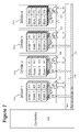
- FIG. 2 shows a first embodiment system 200 .
- a memory system includes memory chips 202 a - 202 d , collectively 202 , which are each attached to one or more circuit boards (not explicitly shown). Each circuit board would create a DIMM.
- a memory system has a motherboard with a set of DIMM sockets, some of which might or might not house a DIMM.
- the memory chips 202 a - 202 d can be distributed over an arbitrary number of DIMMs.
- a typical DIMM might have a data bus that is 72 bits wide while each DRAM has an I/O width of 4 bits. As a result, 18 DRAMs are used to cover the 72 Bits.
- This group of DRAMs is referred to as a rank, since they are all receiving their commands/addresses/controls in parallel.
- the system of FIG. 2 shows four 4 ranks, which can be split over, e.g., one, two or four DIMMs with four, two, or one rank per DIMM, respectively.
- a single chip 202 is illustrated to represent all chips in the rank.
- Other system configurations which could gain advantage from embodiments of the invention, will include 2, 6 and 8 ranks as well.
- the memory chips 202 are coupled to a controller 204 by command bus 206 , control bus 208 , address bus 210 and data bus 212 , which are all typically provided as metal traces in or on the circuit board.
- Each rank of the memory chips 202 has a number of data input/output nodes, e.g., equal to the word length of the bus, coupled to the data bus.
- Each data input/output node is coupled to a programmable termination resistance, which will be discussed in greater detail below. The resistance for each of the programmable termination resistances is determined independently for each chip in a set of memory chips 202 .
- each programmable termination resistance can be determined based on a transaction type and which of the memory chips 202 a - 202 d is communicating with the data bus 212 .
- Other types of information such as DIMM type and/or position on the bus, could additionally or alternatively be issued to determine the programmable termination resistance.
- FIG. 3 illustrates a functional block diagram of each of the memory chips, which are preferably but not necessarily identical.
- each rank of memory chips 202 will typically include a number of chips. While this figure illustrates one configuration for a memory, other configurations could also be used.
- the memory device includes an array of memory cells, such as DRAM cells. In other cases, other types of memory can be utilized.
- an address selection signal ADDR is transmitted to a Column Address Buffer (CAB) 220 and Row Address Buffer (RAB) 224 .
- CAB Column Address Buffer
- RAB Row Address Buffer
- the column address and row address share external pins so that the row address is received at a first time and the column address is received at a second time.
- the ADDR signals may be transmitted by an external device, such as memory controller 204 , for example.
- the column address buffer 220 and row address buffer 224 are adapted to buffer the address signal ADDR.
- the outputs of the column address buffer 220 and row address buffer 224 are coupled to a column decoder 218 and row decoder 222 , respectively.
- the column and row decoders 218 and 222 are adapted to decode the signals received from the column address buffer 220 and row address buffer 224 , respectively, to provide the signal input to the array 216 , such that the selected row and column can be selected.
- the column and row decoders 218 and 222 are shown as single blocks. It should be understood, however, that the column and row decoders 218 and 222 may carry out several levels of predecoding and decoding. Some or all (or none) of these levels may be clocked.
- Data DQ that is addressed in array 216 will be written into the memory or read from the memory via data buffer 226 .
- the data buffer 226 and associated line are provided to represent the read and write path, which may include a large number of lines and other components (e.g., secondary sense amplifiers).
- a programmable termination resistor block 228 is coupled to the data input/output node DQ.
- multiple data input/output lines e.g., four, eight or sixteen, will be included and each will have its own termination resistor.
- the termination resistance can be determined by a transaction type (e.g., read or write) and which of the memory devices 202 a - 202 d is involved in the transaction.
- the programmable termination resistor 228 is set to a termination resistance based on a value stored in the look-up table (element 232 in FIG. 4 ).
- the programmable termination resistor 228 is set by a termination resistance mapping circuit 229 , which will calculate the actual termination setting.
- the circuit 229 can be a programmable table, a set of predetermined tables, a mathematical function or any other circuit to determine the desired resistance value.
- the resistance value determined by the mapping circuit 229 can be based on information received from the bus state determination unit 227 .
- the determination unit 227 is coupled to the ODT bus 214 . While the unit 227 can be a simple receiver coupled to the ODT bus, it could also be a bus snooping unit. For example, in embodiments that do not include an ODT bus, the bus state determination unit could be coupled to an address, command and/or control bus.
- the termination resistance value can be obtained from a transmission control bus 214 .
- the resistance for each of the programmable termination resistances is determined based upon information received from the transmission control bus 214 .
- the finite set of states can be coded and transmitted on a binary transmission control bus 214 that is coupled to all bus participants 202 .
- a 4-bit bus would be sufficient to communicate the complete bus state.
- This 4 bit bus could be formed out of the four ODT signals (one for each DRAM), which have been previously used to control the termination impedance (see control lines 114 in FIG. 1 ).
- the total required number of signals for the bus 214 would not increase compared to existing solutions. Only each bus participant's number of inputs would increase, since one ODT signal would be replaced with the 4-bit transmission state control bus 214 .
- Each bus participant 202 will convert the bus state into a concrete value for the termination impedance.
- One method to do this is a lookup table. For each possible bus state encoded by the bus state control bus 214 , a termination impedance value is stored in the table. Each participant on the bus has a different table with optimum values for this particular point on the bus.
- all possible transmissions modes of a bidirectional multidrop bus channel can be encoded into a binary number and distributed to all bus participants via a transmission control bus 214 .
- the controller 204 is connected to a set of DRAMs, e.g., four ranks of chips in the figure, via a set of busses: unidirectional command, address and control busses 206 , 208 and 210 used to send commands to the DRAMs 202 and a bidirectional data bus 212 used to transfer data from and to the DRAMs 202 .
- Each DRAM 202 has the capability to read and write data from/to the bidirectional data bus 212 .
- the reflections can be different. For example, if the controller 204 is transmitting data, there can be reflections on all four DRAMs, which will arrive at a certain DRAM in a relatively short period of time due to the short bus lengths between the DRAMS. If one of the DRAMs is transmitting data, there are three other DRAMs and the controller 204 to provide reflections, causing a different pattern of disturbance at the receiver.
- reflections can be reduced but not completely eliminated by electrical termination with a resistor on every DRAM 202 . Since it is not possible to completely cancel the reflections, the reflections must be optimized (by adapting the value of the termination resistor) to sum up to the least possible disturbance at the particular receiver. In other words, while individual reflections can be brought close to zero, there are times when a nonzero reflection may be more optimal for the whole system, since it might at least partially cancel other reflections, e.g., the stub reflections. This optimum is different for each transmission scenario (read/write to each individual DRAM).
- the controller 204 knows at any time, which transmission mode the bus is in. In current DRAM memory systems, however, each DRAM does not know the exact bus state since it is only connected to a portion of the control bus. Since the DRAMs need to know the transmission mode to choose the correct termination impedance, the transmission mode needs to be communicated from the controller to the DRAMs. This is done with the transmission control bus 214 in FIG. 2 , which connects all DRAMs 202 with the controller 204 like the command and address busses.
- the coding on this bus can be determined by system needs.
- a binary encoding allows the minimum number of data lines for the bus.
- the relation between the binary numbers and the transmission mode can be chosen to minimize decoding complexity and toggling on the bus.
- Non binary schemes might be feasible as well, if a higher number of data lines for the transmission mode can be traded against lower decoding complexity or power consumption.
- One possible mapping for the 4 DRAM bus is given in the following table:
- the most significant bit encodes, if there is activity (1) on the data bus. If there is no activity (0), all other bits are don't care (x).
- the second most significant bit encodes, if there is a read (0) or a write (1) ongoing. And the two LSBs encode in a binary number, which of the four DRAMs is reading/writing.
- each DRAM 202 contains a programmable table 232 with entries for all possible transmission modes. Each entry contains a value for the termination resistor setting. As shown in FIG. 4 , the settings in the tables 232 of different DRAMs 202 will be different.
- the table 232 is looked up for this mode, information related to the termination resistor value is read out of the table 232 and applied to the termination circuit 228 .
- the lookup table 232 can realized as a register file or SRAM, which is addressed by the encoded value of the transmission control bus.
- the system would include some means to write this register file or SRAM by configuration commands from the controller 204 to the DRAMs 202 during system initialization.
- Each DRAM 202 a - 202 d can be addressed separately for these configuration commands to allow writing different tables into each DRAM.
- FIG. 5 illustrates one possible implementation of the bus state determination circuit 227 , the mapping circuit 229 and the programmable termination resistor 228 .
- the lookup table 232 is stored in a plurality of DRAM mode registers. As noted above, a four rank system will have nine different memory bus transmission states. If the resolution of the resistance values is limited to four bits (i.e., 16 levels), the look up table 232 can be implemented with three 12-bit registers. Of course, in other embodiments, other register configurations and resolutions can be used.
- the specific circuit of FIG. 5 is provided only as an example.
- the contents for the desired look-up table entry 232 are selected using selection circuitry 234 , which in this example is formed from four multiplexers. This particular example corresponds with the embodiment described with respect to the table above. Any selection circuitry, however, could be used for this task.
- the contents of the look up table entry are then provided to the programmable termination resistor 228 .
- four bits are provided to a binary-to-thermometer converter 242 , which outputs fifteen bits.
- the input value read as a binary number denotes the number of active termination fingers. Accordingly, each of the fifteen bits is coupled to select (or not select) a corresponding resistor (or resistor pair) 238 via selection transistor(s) 240 . In this manner, the combination of the individual resistors 238 form a programmable resistor 228 .
- each of the resistors 238 can have the same value R. In this case, the total resistance will scale from no termination (near infinity), to R, R/2, R/3, etc. In other embodiments, the resistors may have different values. As such, the circuit can be designed to provide any fifteen (or sixteen if there is no “no termination” setting) resistance values. In another embodiment, the binary-to-thermometer converter can be avoided and the resistors can selected or not selected independently. Once again, a four bit code would provide sixteen possible resistance values. Alternatively, other numbers of bits can be used. For example, a five-bit code would provide 32 possible resistor values. This modification significantly increases the resolution at the cost of one additional bit for each lookup table entry and more complex decoding, whether using a binary-to-thermometer code or otherwise.
- FIG. 5 is used in a system with a sixteen bit data bus 212 .
- a single lookup table 232 provides the resistance information for sixteen different programmable termination resistors 228 , each programmable termination resistor being coupled to an associated one of the data input/output nodes DQ[15:0].
- each of the DQ nodes would use the same termination resistance.
- an individual lookup table is provided for each input/output node. In this manner, the termination resistance can further be tailored to the specific DQ line.
- schemes described here allow for the optimization of the terminations of the bus signal integrity independently for all possible transmission modes.
- the granularity of values is determined by the resolution of the table entries and not by the system.
- schemes described here separate the termination control completely from the rest of the bus protocol, allowing power efficient implementations.
- a specific memory chip 202 in a low power state does not need to decode commands from the address/command/control busses.
- the channel transmission control bus can be split into two busses 214 a and 214 b , one for the two DRAMs 202 a and 202 b on DIMM 1 and one for the two DRAMs 202 c and 202 d on DIMM 2.
- Each of the two control busses 214 a and 214 b needs to encode fewer combinations and therefore has fewer signals. Even if the total number of bus lines doesn't decrease or even increases, the number of pins on each DRAM component and the complexity of the lookup tables in the components can be reduced.
- This scheme would reduce the table within the DRAM from nine entries to four entries and the number of required transmission state pins on each DRAM from four pins to two pins. There is the restriction, that there is only one termination value for writes, which will be used for reads on the other DIMM as well.
- the lookup table 232 is completely programmable in the most general case. In the case where performance requirements can be traded against implementation complexity, a number of reduction measures are possible. For example, a set of predetermined tables can be provided and then the device can be programmed to determine which table should be used. For example, a pre-programmed table can be selected depending on the position of the participant of the bus. For example, the participant closest to the controller uses the first table, the next closest participant uses the next table and so on.
- FIG. 7 Another embodiment of the invention is provided in FIG. 7 .
- the hard coded table could be programmed during the fabrication process or testing, i.e., before the chips are populated on the DIMM.
- the hard coded tables are programmed after the DIMM is populated. For example, a test procedure can be performed on the DIMM and a one-time programmable ROM or eFuse can be programmed.
- each chip can include only a single look-up table since the position in the DIMM has already been determined. Another simplification technique would be to consolidate multiple similar entries into one entry.
- the dependence of the termination values on the transmission state and some system parameters may be sufficiently deterministic to put it into a mathematical function. Then the table lookup process can be replaced by a circuit for evaluating this mathematical function of the transmission state input and some system parameters, which are set in configuration registers.
- the optimal tables for each participant can be found by simulations or measurements of the particular configuration and statically stored in the system.
- the tables can be determined by a training algorithm during system power up or even with continuous (re-) training during system operation. For example, if the controller knows that the bus will be idle for a period of time, a training algorithm can be performed. In another example, training can be performed when the system determines that performance is lagging or when a physical characteristic such as temperature has changed.
- the controller 204 implements a training algorithm for the termination impedances. This involves some kind of transmission quality monitor at each receiver in the controller 204 and the sets of DRAMs 202 , a mechanism to communicate that quality information to the controller and a search algorithm.
- the controller would initialize the termination tables 232 of all DRAMs 202 to sensible start values. Then it performs transactions on the bus 212 and gets back the transmission quality. Then the values in the termination tables 232 are updated depending on some optimization algorithm (e.g., steepest gradient) and the transaction and quality monitoring procedure is repeated to check for improvements in the data transmission. Depending on the outcome of the measurement the values are modified again until an optimum of transmission quality is achieved.
- the training procedure can be executed if a new memory bus configuration is detected, on every system startup, and/or in regular intervals during system operation.
- the transmission control bus 214 can be extended to a system control bus, which encodes important operation modes of the connected devices.
- this operation mode could be power down.
- the independent signaling of power down with the separate system control bus allows a minimum power overhead for the power down signaling allowing a very low power system solution.
- the transmission control bus information is used to control the command/address/control bus termination.
- the command/address/control bus is statically terminated with a separate resistor at the end of each bus. Each DRAM does not have any termination, which is possibly due to the unidirectional broadcast bus type. This static approach ensures that every DRAM can receive all commands correctly at the expense of spending a lot of power for a low impedance termination and driver. Correct receiving of commands is necessary since any erroneous command leaves the system in an unknown state.
- each DRAM knows whether to receive or ignore the data on the command bus, the command bus could be optimized similar to the data bus.
- Each DRAM (or set of DRAMs) would have a local termination resistor and for each possible transmission mode (idle, command to every DRAM) an optimum termination resistor combination would be chosen to achieve the optimum signal quality at the DRAM, which is supposed to process the command.
- the signal quality can be poor but since the signals are not evaluated no harm will come to the system. This approach would allow the required signal quality to be achieved with less power, since a smaller transmission amplitude is necessary to achieve the same receive data eye height. Only the transmission control bus would need to run in a configuration, which allows error free reception on every DRAM all time.
- bus determination unit 227 does not need to be a receiver for an ODT bus.
- bus determination unit 227 can be a bus snooping unit that determines the transmission state. All traffic on the data bus 212 is controlled by the command, address and control busses 206 - 210 . Thus these three busses contain the information about the data bus transmission state. In contrast to the separate transmission control bus 214 there is a considerable effort to get the actual data bus transmission state from the control/command bus 206 - 210 transaction, i.e., due to variable latencies from a command to a data transfer and a relatively complex encoding of the commands. Furthermore parts of the control bus 208 are not connected to every rank of DRAMs 202 .
- one system that can use a memory system of the present invention is a computer system 250 , an example of which is shown in FIG. 8 .
- the computer system 250 includes a microprocessor 252 which is coupled to a controller 204 .
- controller 204 serves the combined purpose of serving as a memory controller and also as a bus interface controller or bridge. In other systems, separate devices could be used for these tasks.
- the memory system 200 can be any of the memory systems described herein.
- the bus 262 is coupled to a number of components and communicates with the microprocessor 252 via the controller 204 .
- components that can be coupled to the bus 262 are shown, i.e., user input/output 254 (which could include a display, mouse, keyboard, microphone or other), network interface card 256 , hard disk drive 258 and DVD drive 260 . These examples are provided only to show the types of devices that can be utilized in a computer system 250 . Other busses or components could be used.
- the bus 262 shown in FIG. 8 has a number of bus participants. This bus could utilize an on die termination approach as discussed herein.
- each of the bus interface chips would include a control input, e.g. a transmission state control bus 214 , for determining the state of the bus and a programmable resistor as discussed herein.
Landscapes
- Engineering & Computer Science (AREA)
- General Engineering & Computer Science (AREA)
- Theoretical Computer Science (AREA)
- Computer Hardware Design (AREA)
- Physics & Mathematics (AREA)
- General Physics & Mathematics (AREA)
- Dram (AREA)
- Memory System (AREA)
Abstract
Description
| Data bus state | Coding | ||
| Idle | 0xxx | ||
| |
1000 | ||
| |
1001 | ||
| |
1010 | ||
| |
1011 | ||
| |
1100 | ||
| |
1101 | ||
| |
1110 | ||
| |
1111 | ||
| Data Bus state | Coding | ||
| Idle | 00 | ||
| Write to any DRAM, | 01 | ||
| Read to other DIMMs | |||
| DRAMs | |||
| Read on |
10 | ||
| Read on |
11 | ||
Claims (66)
Priority Applications (1)
| Application Number | Priority Date | Filing Date | Title |
|---|---|---|---|
| US12/185,472 US8041865B2 (en) | 2008-08-04 | 2008-08-04 | Bus termination system and method |
Applications Claiming Priority (1)
| Application Number | Priority Date | Filing Date | Title |
|---|---|---|---|
| US12/185,472 US8041865B2 (en) | 2008-08-04 | 2008-08-04 | Bus termination system and method |
Publications (2)
| Publication Number | Publication Date |
|---|---|
| US20100030934A1 US20100030934A1 (en) | 2010-02-04 |
| US8041865B2 true US8041865B2 (en) | 2011-10-18 |
Family
ID=41609472
Family Applications (1)
| Application Number | Title | Priority Date | Filing Date |
|---|---|---|---|
| US12/185,472 Active 2028-12-23 US8041865B2 (en) | 2008-08-04 | 2008-08-04 | Bus termination system and method |
Country Status (1)
| Country | Link |
|---|---|
| US (1) | US8041865B2 (en) |
Cited By (10)
| Publication number | Priority date | Publication date | Assignee | Title |
|---|---|---|---|---|
| US20100142287A1 (en) * | 2005-12-16 | 2010-06-10 | Micron Technology, Inc. | System and method for providing temperature data from a memory device having a temperature sensor |
| US20120182044A1 (en) * | 2009-10-01 | 2012-07-19 | Rambus Inc. | Methods and Systems for Reducing Supply and Termination Noise |
| US9214939B2 (en) * | 2013-12-02 | 2015-12-15 | Texas Instruments Deutschland Gmbh | Adaptive bus termination apparatus and methods |
| US9292391B2 (en) * | 2014-02-12 | 2016-03-22 | Apple Inc. | Interface calibration using configurable on-die terminations |
| CN106575272A (en) * | 2014-08-11 | 2017-04-19 | 高通股份有限公司 | Memory circuit configuration schemes on multi-drop buses |
| US9978460B2 (en) | 2015-12-22 | 2018-05-22 | Samsung Electronics Co., Ltd. | Memory module including on-die termination circuit and control method thereof |
| US20210377060A1 (en) * | 2020-05-26 | 2021-12-02 | Nxp B.V. | Controller area network controller and transceiver |
| US11475930B2 (en) * | 2017-05-29 | 2022-10-18 | Samsung Electronics Co., Ltd. | Method of controlling on-die termination and system performing the same |
| US11502876B2 (en) * | 2018-03-12 | 2022-11-15 | Robert Bosch Gmbh | Transceiver device for a bus system and operating method therefor |
| US11750190B2 (en) | 2020-12-14 | 2023-09-05 | Intel Corporation | Encoded on-die termination for efficient multipackage termination |
Families Citing this family (12)
| Publication number | Priority date | Publication date | Assignee | Title |
|---|---|---|---|---|
| US7843213B1 (en) * | 2009-05-21 | 2010-11-30 | Nanya Technology Corp. | Signal termination scheme for high speed memory modules |
| US8988102B2 (en) | 2011-02-02 | 2015-03-24 | Rambus Inc. | On-die termination |
| US9281816B2 (en) | 2012-01-31 | 2016-03-08 | Rambus Inc. | Modulated on-die termination |
| US9798628B2 (en) | 2014-04-25 | 2017-10-24 | Rambus Inc. | Memory mirroring |
| DE102014222661B4 (en) | 2014-11-06 | 2026-03-26 | Siemens Schweiz Ag | Arrangement and method for optimizing the transmission of digital data in two-wire communication networks |
| US10282340B2 (en) | 2014-12-17 | 2019-05-07 | The Boeing Company | Pin-configurable internal bus termination system |
| US11068433B2 (en) * | 2018-10-18 | 2021-07-20 | Texas Instruments Incorporated | Serial bus repeater with low power state detection |
| DE102018132438B3 (en) * | 2018-12-17 | 2020-02-13 | Schölly Fiberoptic GmbH | Method of building a video bus, video bus arrangement, plug-in card and corresponding use |
| US11238909B2 (en) * | 2019-08-14 | 2022-02-01 | Micron Technology, Inc. | Apparatuses and methods for setting operational parameters of a memory included in a memory module based on location information |
| JP2022051374A (en) * | 2020-09-18 | 2022-03-31 | キオクシア株式会社 | Semiconductor storage device and writing method for operation control program for semiconductor storage device |
| KR20220112322A (en) * | 2021-02-03 | 2022-08-11 | 삼성전자주식회사 | Interface circuit that controlling output impedance of transmitting circuit and image sensor including the same |
| CN114721593B (en) * | 2022-03-18 | 2024-10-15 | 苏州浪潮智能科技有限公司 | Storage device information collection method, system and electronic device |
Citations (22)
| Publication number | Priority date | Publication date | Assignee | Title |
|---|---|---|---|---|
| US5467455A (en) * | 1993-11-03 | 1995-11-14 | Motorola, Inc. | Data processing system and method for performing dynamic bus termination |
| US6356106B1 (en) * | 2000-09-12 | 2002-03-12 | Micron Technology, Inc. | Active termination in a multidrop memory system |
| US20030039151A1 (en) * | 2001-08-24 | 2003-02-27 | Yoshinori Matsui | Memory device and memory system |
| US6538951B1 (en) * | 2001-08-30 | 2003-03-25 | Micron Technology, Inc. | Dram active termination control |
| US20030126338A1 (en) * | 2001-12-31 | 2003-07-03 | Dodd James M. | Memory bus termination with memory unit having termination control |
| US6642740B2 (en) * | 2000-09-15 | 2003-11-04 | Samsung Electronics Co., Ltd. | Programmable termination circuit and method |
| US20030234664A1 (en) * | 2002-06-20 | 2003-12-25 | Mitsubishi Denki Kabushiki Kaisha | Data bus |
| US20040098528A1 (en) * | 2002-11-20 | 2004-05-20 | Micron Technology, Inc. | Active termination control though on module register |
| US6762620B2 (en) * | 2002-05-24 | 2004-07-13 | Samsung Electronics Co., Ltd. | Circuit and method for controlling on-die signal termination |
| US6834014B2 (en) * | 2001-07-20 | 2004-12-21 | Samsung Electronics Co., Ltd. | Semiconductor memory systems, methods, and devices for controlling active termination |
| US6922076B2 (en) * | 2003-08-27 | 2005-07-26 | International Business Machines Corporation | Scalable termination |
| US7020818B2 (en) | 2004-03-08 | 2006-03-28 | Intel Corporation | Method and apparatus for PVT controller for programmable on die termination |
| US7157932B2 (en) * | 2004-11-30 | 2007-01-02 | Agere Systems Inc. | Adjusting settings of an I/O circuit for process, voltage, and/or temperature variations |
| US20070035326A1 (en) * | 2005-07-29 | 2007-02-15 | Georg Braun | Memory chip and method for operating a memory chip |
| US7414426B2 (en) * | 2005-12-07 | 2008-08-19 | Intel Corporation | Time multiplexed dynamic on-die termination |
| US7433992B2 (en) * | 2004-11-18 | 2008-10-07 | Intel Corporation | Command controlling different operations in different chips |
| US7516281B2 (en) * | 2004-05-25 | 2009-04-07 | Micron Technology, Inc. | On-die termination snooping for 2T applications in a memory system implementing non-self-terminating ODT schemes |
| US7554353B2 (en) * | 2006-06-16 | 2009-06-30 | Samsung Electronics Co., Ltd. | Method of controlling on-die termination of memory devices sharing signal lines |
| US20090230989A1 (en) * | 2006-10-18 | 2009-09-17 | Canon Kabushiki Kaisha | Memory control circuit, memory control method, and integrated circuit |
| US7602209B2 (en) * | 2006-06-02 | 2009-10-13 | Rambus Inc. | Controlling memory devices that have on-die termination |
| US20090273960A1 (en) * | 2008-04-30 | 2009-11-05 | International Business Machines Corporation | System for providing on-die termination of a control signal bus |
| US7616473B2 (en) * | 2002-08-17 | 2009-11-10 | Samsung Electronics Co., Ltd. | Devices and methods for controlling active termination resistors in a memory system |
-
2008
- 2008-08-04 US US12/185,472 patent/US8041865B2/en active Active
Patent Citations (22)
| Publication number | Priority date | Publication date | Assignee | Title |
|---|---|---|---|---|
| US5467455A (en) * | 1993-11-03 | 1995-11-14 | Motorola, Inc. | Data processing system and method for performing dynamic bus termination |
| US6356106B1 (en) * | 2000-09-12 | 2002-03-12 | Micron Technology, Inc. | Active termination in a multidrop memory system |
| US6642740B2 (en) * | 2000-09-15 | 2003-11-04 | Samsung Electronics Co., Ltd. | Programmable termination circuit and method |
| US6834014B2 (en) * | 2001-07-20 | 2004-12-21 | Samsung Electronics Co., Ltd. | Semiconductor memory systems, methods, and devices for controlling active termination |
| US20030039151A1 (en) * | 2001-08-24 | 2003-02-27 | Yoshinori Matsui | Memory device and memory system |
| US6538951B1 (en) * | 2001-08-30 | 2003-03-25 | Micron Technology, Inc. | Dram active termination control |
| US20030126338A1 (en) * | 2001-12-31 | 2003-07-03 | Dodd James M. | Memory bus termination with memory unit having termination control |
| US6762620B2 (en) * | 2002-05-24 | 2004-07-13 | Samsung Electronics Co., Ltd. | Circuit and method for controlling on-die signal termination |
| US20030234664A1 (en) * | 2002-06-20 | 2003-12-25 | Mitsubishi Denki Kabushiki Kaisha | Data bus |
| US7616473B2 (en) * | 2002-08-17 | 2009-11-10 | Samsung Electronics Co., Ltd. | Devices and methods for controlling active termination resistors in a memory system |
| US20040098528A1 (en) * | 2002-11-20 | 2004-05-20 | Micron Technology, Inc. | Active termination control though on module register |
| US6922076B2 (en) * | 2003-08-27 | 2005-07-26 | International Business Machines Corporation | Scalable termination |
| US7020818B2 (en) | 2004-03-08 | 2006-03-28 | Intel Corporation | Method and apparatus for PVT controller for programmable on die termination |
| US7516281B2 (en) * | 2004-05-25 | 2009-04-07 | Micron Technology, Inc. | On-die termination snooping for 2T applications in a memory system implementing non-self-terminating ODT schemes |
| US7433992B2 (en) * | 2004-11-18 | 2008-10-07 | Intel Corporation | Command controlling different operations in different chips |
| US7157932B2 (en) * | 2004-11-30 | 2007-01-02 | Agere Systems Inc. | Adjusting settings of an I/O circuit for process, voltage, and/or temperature variations |
| US20070035326A1 (en) * | 2005-07-29 | 2007-02-15 | Georg Braun | Memory chip and method for operating a memory chip |
| US7414426B2 (en) * | 2005-12-07 | 2008-08-19 | Intel Corporation | Time multiplexed dynamic on-die termination |
| US7602209B2 (en) * | 2006-06-02 | 2009-10-13 | Rambus Inc. | Controlling memory devices that have on-die termination |
| US7554353B2 (en) * | 2006-06-16 | 2009-06-30 | Samsung Electronics Co., Ltd. | Method of controlling on-die termination of memory devices sharing signal lines |
| US20090230989A1 (en) * | 2006-10-18 | 2009-09-17 | Canon Kabushiki Kaisha | Memory control circuit, memory control method, and integrated circuit |
| US20090273960A1 (en) * | 2008-04-30 | 2009-11-05 | International Business Machines Corporation | System for providing on-die termination of a control signal bus |
Non-Patent Citations (5)
| Title |
|---|
| "DDR2 Application Note ODT(On Die Termination) Control," Samsung Electronics Co. Ltd., Mar. 2006, 12 pages. |
| "New Function of DDR2 SDRAM On Die Termination (ODT)," Technical Note, Elpida Memory Inc., Jan. 2005, 12 pages. |
| "On Die Termination (ODT) Calibration," Rambus, 2008, 8 pages. |
| "On-Die Termination," Wikipedia, the Free Encyclopedia, 3 pages, http://en.wikipedia.org/wiki/On-die-termination. |
| "Proper Termination for High-Speed Digital I/O Applications," NI Developer Zone, National Instruments, Sep. 6, 2006, 4 pages. |
Cited By (14)
| Publication number | Priority date | Publication date | Assignee | Title |
|---|---|---|---|---|
| US20100142287A1 (en) * | 2005-12-16 | 2010-06-10 | Micron Technology, Inc. | System and method for providing temperature data from a memory device having a temperature sensor |
| US8186878B2 (en) * | 2005-12-16 | 2012-05-29 | Round Rock Research, Llc | System and method for providing temperature data from a memory device having a temperature sensor |
| US20120182044A1 (en) * | 2009-10-01 | 2012-07-19 | Rambus Inc. | Methods and Systems for Reducing Supply and Termination Noise |
| US8692574B2 (en) * | 2009-10-01 | 2014-04-08 | Rambus Inc. | Methods and systems for reducing supply and termination noise |
| US9059695B2 (en) | 2009-10-01 | 2015-06-16 | Rambus Inc. | Methods and systems for reducing supply and termination noise |
| US9214939B2 (en) * | 2013-12-02 | 2015-12-15 | Texas Instruments Deutschland Gmbh | Adaptive bus termination apparatus and methods |
| US9292391B2 (en) * | 2014-02-12 | 2016-03-22 | Apple Inc. | Interface calibration using configurable on-die terminations |
| CN106575272A (en) * | 2014-08-11 | 2017-04-19 | 高通股份有限公司 | Memory circuit configuration schemes on multi-drop buses |
| US9978460B2 (en) | 2015-12-22 | 2018-05-22 | Samsung Electronics Co., Ltd. | Memory module including on-die termination circuit and control method thereof |
| US11475930B2 (en) * | 2017-05-29 | 2022-10-18 | Samsung Electronics Co., Ltd. | Method of controlling on-die termination and system performing the same |
| US11502876B2 (en) * | 2018-03-12 | 2022-11-15 | Robert Bosch Gmbh | Transceiver device for a bus system and operating method therefor |
| US20210377060A1 (en) * | 2020-05-26 | 2021-12-02 | Nxp B.V. | Controller area network controller and transceiver |
| US11722327B2 (en) * | 2020-05-26 | 2023-08-08 | Nxp B.V. | Controller area network controller and transceiver |
| US11750190B2 (en) | 2020-12-14 | 2023-09-05 | Intel Corporation | Encoded on-die termination for efficient multipackage termination |
Also Published As
| Publication number | Publication date |
|---|---|
| US20100030934A1 (en) | 2010-02-04 |
Similar Documents
| Publication | Publication Date | Title |
|---|---|---|
| US8041865B2 (en) | Bus termination system and method | |
| US12235760B2 (en) | Apparatus having selectively-activated termination circuitry | |
| US8391088B2 (en) | Pseudo-open drain type output driver having de-emphasis function, semiconductor memory device, and control method thereof | |
| US6834014B2 (en) | Semiconductor memory systems, methods, and devices for controlling active termination | |
| US10033382B2 (en) | Method and apparatus for dynamic memory termination | |
| CN111009269B (en) | Apparatus and method for storing and writing multiple parameter codes of memory operating parameters | |
| KR100951091B1 (en) | Integrated circuits, methods and systems | |
| EP3394856B1 (en) | Flexible dll (delay locked loop) calibration | |
| US7342411B2 (en) | Dynamic on-die termination launch latency reduction | |
| US7864604B2 (en) | Multiple address outputs for programming the memory register set differently for different DRAM devices | |
| US20130346684A1 (en) | Method, apparatus and system for a per-dram addressability mode | |
| US20080197877A1 (en) | Per byte lane dynamic on-die termination | |
| US20200293197A1 (en) | Memory device | |
| CN101169772A (en) | Method and apparatus for transmitting command and address signals | |
| EP3767430A1 (en) | Techniques to adapt dc bias of voltage regulators for memory devices as a function of bandwidth demand | |
| US7840744B2 (en) | Rank select operation between an XIO interface and a double data rate interface | |
| CN114187934A (en) | Semiconductor memory | |
| US20170287538A1 (en) | Flexible point-to-point memory topology | |
| CN110659228B (en) | Memory system and method for accessing memory system | |
| KR100942947B1 (en) | Semiconductor memory device | |
| KR102545175B1 (en) | Operating method of memeory device including address table and memory controller thereof | |
| US7898883B2 (en) | Method for controlling access of a memory | |
| CN117195820A (en) | Design method and equipment of DDR (double data rate) expansion circuit in board-mounted memory mode | |
| US20120191898A1 (en) | Ddr flash implementation with direct register access to legacy flash functions | |
| US7013374B2 (en) | Integrated memory and method for setting the latency in the integrated memory |
Legal Events
| Date | Code | Title | Description |
|---|---|---|---|
| AS | Assignment |
Owner name: QIMONDA NORTH AMERICA CORP.,NORTH CAROLINA Free format text: ASSIGNMENT OF ASSIGNORS INTEREST;ASSIGNOR:ALEXANDER, GEORGE;REEL/FRAME:021336/0421 Effective date: 20080721 Owner name: QIMONDA AG,GERMANY Free format text: ASSIGNMENT OF ASSIGNORS INTEREST;ASSIGNORS:BRUENNERT, MICHAEL;GREGORIUS, PETER;BRAUN, GEORG;AND OTHERS;SIGNING DATES FROM 20080724 TO 20080804;REEL/FRAME:021336/0489 Owner name: QIMONDA NORTH AMERICA CORP., NORTH CAROLINA Free format text: ASSIGNMENT OF ASSIGNORS INTEREST;ASSIGNOR:ALEXANDER, GEORGE;REEL/FRAME:021336/0421 Effective date: 20080721 Owner name: QIMONDA AG, GERMANY Free format text: ASSIGNMENT OF ASSIGNORS INTEREST;ASSIGNORS:BRUENNERT, MICHAEL;GREGORIUS, PETER;BRAUN, GEORG;AND OTHERS;SIGNING DATES FROM 20080724 TO 20080804;REEL/FRAME:021336/0489 |
|
| FEPP | Fee payment procedure |
Free format text: PAYOR NUMBER ASSIGNED (ORIGINAL EVENT CODE: ASPN); ENTITY STATUS OF PATENT OWNER: LARGE ENTITY |
|
| AS | Assignment |
Owner name: QIMONDA AG, GERMANY Free format text: ASSIGNMENT OF ASSIGNORS INTEREST;ASSIGNOR:QIMONDA NORTH AMERICA CORP.;REEL/FRAME:026144/0905 Effective date: 20110221 |
|
| STCF | Information on status: patent grant |
Free format text: PATENTED CASE |
|
| FPAY | Fee payment |
Year of fee payment: 4 |
|
| AS | Assignment |
Owner name: INFINEON TECHNOLOGIES AG, GERMANY Free format text: ASSIGNMENT OF ASSIGNORS INTEREST;ASSIGNOR:QIMONDA AG;REEL/FRAME:035623/0001 Effective date: 20141009 |
|
| AS | Assignment |
Owner name: POLARIS INNOVATIONS LIMITED, IRELAND Free format text: ASSIGNMENT OF ASSIGNORS INTEREST;ASSIGNOR:INFINEON TECHNOLOGIES AG;REEL/FRAME:036575/0670 Effective date: 20150708 |
|
| MAFP | Maintenance fee payment |
Free format text: PAYMENT OF MAINTENANCE FEE, 8TH YEAR, LARGE ENTITY (ORIGINAL EVENT CODE: M1552); ENTITY STATUS OF PATENT OWNER: LARGE ENTITY Year of fee payment: 8 |
|
| MAFP | Maintenance fee payment |
Free format text: PAYMENT OF MAINTENANCE FEE, 12TH YEAR, LARGE ENTITY (ORIGINAL EVENT CODE: M1553); ENTITY STATUS OF PATENT OWNER: LARGE ENTITY Year of fee payment: 12 |