US8027210B2 - Data input apparatus with improved setup/hold window - Google Patents
Data input apparatus with improved setup/hold window Download PDFInfo
- Publication number
- US8027210B2 US8027210B2 US12/199,046 US19904608A US8027210B2 US 8027210 B2 US8027210 B2 US 8027210B2 US 19904608 A US19904608 A US 19904608A US 8027210 B2 US8027210 B2 US 8027210B2
- Authority
- US
- United States
- Prior art keywords
- signal
- data
- test mode
- unit
- input apparatus
- Prior art date
- Legal status (The legal status is an assumption and is not a legal conclusion. Google has not performed a legal analysis and makes no representation as to the accuracy of the status listed.)
- Expired - Fee Related, expires
Links
Images


Classifications
-
- G—PHYSICS
- G11—INFORMATION STORAGE
- G11C—STATIC STORES
- G11C11/00—Digital stores characterised by the use of particular electric or magnetic storage elements; Storage elements therefor
- G11C11/21—Digital stores characterised by the use of particular electric or magnetic storage elements; Storage elements therefor using electric elements
- G11C11/34—Digital stores characterised by the use of particular electric or magnetic storage elements; Storage elements therefor using electric elements using semiconductor devices
- G11C11/40—Digital stores characterised by the use of particular electric or magnetic storage elements; Storage elements therefor using electric elements using semiconductor devices using transistors
- G11C11/401—Digital stores characterised by the use of particular electric or magnetic storage elements; Storage elements therefor using electric elements using semiconductor devices using transistors forming cells needing refreshing or charge regeneration, i.e. dynamic cells
- G11C11/4063—Auxiliary circuits, e.g. for addressing, decoding, driving, writing, sensing or timing
- G11C11/407—Auxiliary circuits, e.g. for addressing, decoding, driving, writing, sensing or timing for memory cells of the field-effect type
- G11C11/409—Read-write [R-W] circuits
- G11C11/4093—Input/output [I/O] data interface arrangements, e.g. data buffers
-
- G—PHYSICS
- G11—INFORMATION STORAGE
- G11C—STATIC STORES
- G11C7/00—Arrangements for writing information into, or reading information out from, a digital store
- G11C7/10—Input/output [I/O] data interface arrangements, e.g. I/O data control circuits, I/O data buffers
- G11C7/1072—Input/output [I/O] data interface arrangements, e.g. I/O data control circuits, I/O data buffers for memories with random access ports synchronised on clock signal pulse trains, e.g. synchronous memories, self timed memories
-
- G—PHYSICS
- G11—INFORMATION STORAGE
- G11C—STATIC STORES
- G11C11/00—Digital stores characterised by the use of particular electric or magnetic storage elements; Storage elements therefor
- G11C11/21—Digital stores characterised by the use of particular electric or magnetic storage elements; Storage elements therefor using electric elements
- G11C11/34—Digital stores characterised by the use of particular electric or magnetic storage elements; Storage elements therefor using electric elements using semiconductor devices
- G11C11/40—Digital stores characterised by the use of particular electric or magnetic storage elements; Storage elements therefor using electric elements using semiconductor devices using transistors
- G11C11/401—Digital stores characterised by the use of particular electric or magnetic storage elements; Storage elements therefor using electric elements using semiconductor devices using transistors forming cells needing refreshing or charge regeneration, i.e. dynamic cells
- G11C11/4063—Auxiliary circuits, e.g. for addressing, decoding, driving, writing, sensing or timing
- G11C11/407—Auxiliary circuits, e.g. for addressing, decoding, driving, writing, sensing or timing for memory cells of the field-effect type
- G11C11/409—Read-write [R-W] circuits
- G11C11/4096—Input/output [I/O] data management or control circuits, e.g. reading or writing circuits, I/O drivers or bit-line switches
-
- G—PHYSICS
- G11—INFORMATION STORAGE
- G11C—STATIC STORES
- G11C7/00—Arrangements for writing information into, or reading information out from, a digital store
- G11C7/10—Input/output [I/O] data interface arrangements, e.g. I/O data control circuits, I/O data buffers
- G11C7/1078—Data input circuits, e.g. write amplifiers, data input buffers, data input registers, data input level conversion circuits
- G11C7/1084—Data input buffers, e.g. comprising level conversion circuits, circuits for adapting load
-
- G—PHYSICS
- G11—INFORMATION STORAGE
- G11C—STATIC STORES
- G11C7/00—Arrangements for writing information into, or reading information out from, a digital store
- G11C7/10—Input/output [I/O] data interface arrangements, e.g. I/O data control circuits, I/O data buffers
- G11C7/1078—Data input circuits, e.g. write amplifiers, data input buffers, data input registers, data input level conversion circuits
- G11C7/109—Control signal input circuits
-
- G—PHYSICS
- G11—INFORMATION STORAGE
- G11C—STATIC STORES
- G11C7/00—Arrangements for writing information into, or reading information out from, a digital store
- G11C7/10—Input/output [I/O] data interface arrangements, e.g. I/O data control circuits, I/O data buffers
- G11C7/1078—Data input circuits, e.g. write amplifiers, data input buffers, data input registers, data input level conversion circuits
- G11C7/1093—Input synchronization
-
- G—PHYSICS
- G11—INFORMATION STORAGE
- G11C—STATIC STORES
- G11C7/00—Arrangements for writing information into, or reading information out from, a digital store
- G11C7/22—Read-write [R-W] timing or clocking circuits; Read-write [R-W] control signal generators or management
-
- G—PHYSICS
- G11—INFORMATION STORAGE
- G11C—STATIC STORES
- G11C7/00—Arrangements for writing information into, or reading information out from, a digital store
- G11C7/22—Read-write [R-W] timing or clocking circuits; Read-write [R-W] control signal generators or management
- G11C7/225—Clock input buffers
-
- G—PHYSICS
- G11—INFORMATION STORAGE
- G11C—STATIC STORES
- G11C8/00—Arrangements for selecting an address in a digital store
- G11C8/06—Address interface arrangements, e.g. address buffers
-
- G—PHYSICS
- G11—INFORMATION STORAGE
- G11C—STATIC STORES
- G11C8/00—Arrangements for selecting an address in a digital store
- G11C8/18—Address timing or clocking circuits; Address control signal generation or management, e.g. for row address strobe [RAS] or column address strobe [CAS] signals
Definitions
- the present invention relates to a semiconductor memory device, and more particularly, to a data input apparatus in a semiconductor memory device.
- Semiconductor memory devices are being continuously improved in order to increase the degree of integration and improve the operation speed.
- a synchronous memory device that can be operated in synchronization with a clock provided externally from a memory chip has been proposed.
- One such proposed synchronous memory device is a single data rate (SDR) synchronous memory device that is synchronized with a rising edge of the clock provided from the external of the memory device to input and output a single data over a single period.
- SDR single data rate
- DDR double data rate
- FIG. 1 is a block view schematically showing blocks associated with a write operation of the conventional DDR synchronous memory device.
- the semiconductor memory device comprises: a data strobe buffer 10 receiving and buffering data strobe signals DQS and DQSB; a data strobe driver 12 driving a signal outputted from the data strobe buffer 10 to output a rising strobe pulse DQSRP and a falling strobe pulse DQSFP; a data input buffer 14 buffering data DQ inputted through a data input/output pad, a data delay unit 16 delaying an output signal of the data input buffer for a predetermined time and outputting an output signal; and a data alignment unit 18 latching input data DIN outputted from the data delay unit in synchronization with the data strobe signal to align them.
- the rising data strobe pulse DQSRP is a signal synchronized with the rising edge of the data strobe signal DQS
- the falling data strobe pulse DQSFP is a signal synchronized with the falling edge of the data strobe signal DQS.
- the delay unit 16 delays the buffered data by a predetermined time and allocates the input data DIN to the data alignment unit 18 .
- the data alignment unit 18 aligns the input data DIN by synchronizing the input data DIN with the rising data strobe pulse DQSRP and the falling data strobe pulse DQSFP.
- the data aligned by the data alignment unit 18 is transferred to a memory cell region via a global input/output line in response to a pulse applied from the external.
- FIG. 2 is a timing diagram for explaining the operation of FIG. 1 .
- FIG. 2 confirms that the rising data strobe pulse DQSRP is synchronized with the rising edge of the data strobe signal DQS and the falling data strobe pulse DQSFP is synchronized with the falling edge of the data strobe signal DQS.
- the data DIN inputted to the data alignment unit 18 is delayed through the delay unit 16 to secure a setup/hold time.
- FIG. 3 shows a prior art method of turning-off the data strobe buffer upon entering into a test mode and aligning the data using the output of a clock buffer.
- the semiconductor device comprises a data strobe buffer 30 , a data strobe driver 32 , a data input buffer 34 , a data delay unit 36 , a data alignment unit 38 , and a clock buffer 40 .
- the clock buffer 40 buffers an external clock signal pair CLK and CLKB that is inputted from outside to output an internal clock signal BCK.
- the data strobe buffer 30 and the data strobe driver 32 have a similar configuration to the buffer 10 and the driver 12 as shown in FIG. 1 ; however, there is a difference, in that the data strobe buffer 30 and the data strobe driver 32 are operated in response to a test mode signal TM. That is, the data strobe buffer 30 and the data strobe driver 32 are turned-off upon entering into a test mode, in which the test mode signal TM is enabled.
- the data strobe driver is synchronized with the internal clock signal BCK outputted from the clock buffer in order to output the data strobe pulse DQSRP and the falling data strobe pulse DQSFP.
- the rising data strobe pulse DQSRP is outputted in synchronization with the rising edge of the internal clock signal BCK
- the falling data strobe pulse DQSFP is outputted in synchronization with the falling edge of the internal clock signal BCK.
- the data delay unit 36 and the data alignment unit 38 are operated identically to the data delay unit 16 and the data alignment unit 18 shown in FIG. 1 ; and therefore, a detailed description will be omitted.
- the clock buffer 40 is distributed at the center of the chip
- the data strobe buffer 30 and the data strobe driver 32 are distributed at the left of the chip
- the data block (DQ pad, data input buffer, data delay unit, data alignment unit) is distributed at the left-center of the chip.
- the output signal BCK of the clock buffer is input to the data block via the data strobe driver 32 , and thus the moving path of the signals is long, and it takes much more time for the internal clock signal BCK to be input to the data block. Accordingly, it is more difficult to secure the data setup/hold time margins in the semiconductor device shown in FIG. 3 .
- FIG. 4 is a timing diagram for explaining the operation of FIG. 3 . Referring to FIG. 4 , the problems can be more obviously confirmed.
- FIG. 4 confirms that when the semiconductor device shown in FIG. 3 is operated in a test mode, the setup/hold time window characteristics are different from that of the semiconductor memory device when it is operated normally.
- the test mode TM is enabled at a high level turning off the data strobe buffer 30 and the data strobe driver 32 .
- the pulse signals DQSRP and DQSFP are synchronized with the rising edge and falling edge of the internal clock signal BLCK respectively.
- FIG. 4 shows that the pulse signals DQSRP and DQSFP are delayed more than the input data DIN (which is delayed by the data delay unit 36 ).
- the amount of delay delayed by the data delay unit 36 is increased so that the setup time conforms to the hold time when the semiconductor device is in the test mode, problems occur when the semiconductor device operates in a non-test mode (i.e., normal mode).
- a non-test mode i.e., normal mode
- the data strobe buffer 30 and the data strobe driver 32 are operated normally; and therefore, the amount of delay cannot be increased based on the problems incurred when the semiconductor device is in the test mode.
- the present invention provides a data input apparatus in a semiconductor memory device capable of improving a setup/hold time window in a test mode.
- the present invention provides a data input apparatus capable of improving productivity by reducing the number of pins required in test equipment when testing a semiconductor memory device.
- the present invention provides a data input apparatus capable of increasing signal transmission efficiency and improving a data setup/hold time window since the output signal of the clock buffer in the present invention is not passed through a data strobe driver when the semiconductor device is in a test mode.
- the present invention controls the degree of delaying of data inputted from the external by a test mode signal.
- a data input apparatus comprises: a data delay unit delaying and outputting data inputted from outside the data input apparatus, wherein the degree of delay differs according to a test mode signal; a data alignment signal generating unit receiving a first signal synchronized with an external clock signal and receiving a second signal synchronized with a data strobe signal to output any one of the first signal and the second signal as a data alignment signal in response to the test mode signal; and a data alignment unit synchronized with the data alignment signal to align the data delayed in the data delay unit.
- the data alignment signal generating unit outputs the data alignment signal synchronized with the first signal when the test mode signal is enabled and outputs the data alignment signal synchronized with the second signal when the test mode signal is disabled.
- the data alignment signal generating unit comprises a rising data alignment signal output unit to output a rising data alignment signal synchronized with a rising edge of the first signal or a rising data alignment signal synchronized with a rising edge of the second signal and a falling data alignment signal output unit to output a falling data alignment signal synchronized with a falling edge of the first signal or a falling data alignment signal synchronized with a falling edge of the second signal in response to the test mode signal.
- the second signal comprises a rising data strobe pulse synchronized with the rising edge of the data strobe signal and a falling data strobe pulse synchronized with the falling edge of the data strobe signal.
- the rising data alignment signal output unit outputs the first signal when the test mode signal is enabled and outputs the rising data strobe pulse when the test mode signal is disabled.
- the falling data alignment signal output unit outputs an inverted first signal when the test mode signal is enabled and outputs the falling data strobe pulse when the test mode signal is disabled.
- the degree of delay delayed by the data delay unit is higher when the test mode signal is enabled than the degree of delay delayed by the delay unit when the test mode signal is disabled.
- the data delay unit is arranged adjacent to the data alignment unit when the signal selection unit is disposed in the data input apparatus.
- a data input apparatus comprises a data strobe buffer unit receiving and buffering a data strobe signal in response to a test mode signal to output a rising data strobe signal and a falling data strobe signal; a data delay unit delaying and outputting data inputted from outside the data input apparatus, wherein the degree of delay differs according to the test mode signal; a clock buffer unit buffering an external clock signal to output an internal clock signal; a signal selection unit selecting one of the rising data strobe signal and the internal clock signal and selecting one of the falling data strobe signal and an inverted internal clock signal, the signals being selected in accordance with the test mode signal, and outputting the selected signals as a data alignment signal; and a data alignment unit synchronized with the data alignment signal to align input data outputted from the data delay unit.
- an input pin receiving the data strobe signal may be connected to a ground voltage or floated.
- the signal selection unit selects the internal clock signal and the inverted internal clock signal to be output as the data alignment signal when the test mode signal is enabled.
- the signal selection unit selects the rising data strobe signal and the falling data strobe signal to be output as the data alignment signal when the test mode signal is disabled.
- the signal selection unit may comprises a rising data alignment signal output unit outputting one of the rising data strobe signal and the internal clock signal in response to the test mode signal; a the falling data alignment signal output unit outputting one of the falling data strobe signal and the inverted internal clock signal in response to the test mode signal.
- the rising data alignment signal output unit may comprises a first transfer unit transferring the rising data strobe signal when the test mode signal is disabled and transferring the internal clock signal when the test mode signal is enabled.
- the falling data alignment signal output unit may comprise a second transfer unit transferring the falling data strobe signal when the test mode signal is disabled and transferring the inverted internal clock signal when the test mode signal is enabled.
- the signal selection unit is arranged adjacent to the data alignment unit when the signal selection unit is disposed in the data input apparatus.
- the degree of delay that the data delay unit delays the signal outputted from the data input buffer is enough to secure setup and hold time window margins of the data when the test mode signal is enabled.
- the data delay unit may include a third transfer unit that transfers the delayed data when the test mode signal is enabled.
- a data input apparatus comprises a buffer region comprising a data strobe buffer unit buffering a data strobe signal to output a strobe signal and a clock buffer unit buffering an external clock signal to output an internal clock signal; a signal selection region comprising a signal selection unit selecting any one of the strobe signal and the internal clock signal to apply the selected signal to a data block; and a data region comprising a data block buffering data inputted from outside the data input apparatus, the data block being synchronized with one of the strobe signal and the internal clock signal to align the data, wherein the buffer region, the signal selection region, and the data region are sequentially formed, and wherein the signal selection unit is arranged in the signal selection region such that the signal selection unit is between the data strobe buffer unit and the clock buffer unit.
- the signal selection unit arranged between the clock buffer unit and the data block is adjacent to the data block, such that the data inputted from the clock buffer is inputted to the data block via the shortest path.
- FIG. 1 is a block view of a prior art data input apparatus
- FIG. 2 is a timing diagram showing the operation of FIG. 1 ;
- FIG. 3 is a block view of another prior art data input apparatus
- FIG. 4 is a timing diagram showing the operation of FIG. 3 ;
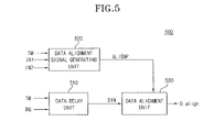
- FIG. 5 is a block view of a data input apparatus according to one embodiment of the present invention.
- FIG. 6 is a block view of a data input apparatus according to another embodiment of the present invention.
- FIG. 7 is a detailed circuit diagram of the data delay unit of FIG. 6 .
- FIG. 8 is a detailed circuit diagram of the signal selection unit of FIG. 6 .
- FIG. 9 is a block view of the data alignment unit of FIG. 6 .
- FIG. 10 is a detailed circuit diagram of the first latch unit of FIG. 9 .
- FIG. 11 is a timing diagram showing the operation of the data input apparatus of FIG. 6 .
- FIG. 12 is a block view showing the positioning of the signal selection unit of FIG. 6 . as arranged in the data input apparatus.
- the present invention discloses: a method capable of improving a data setup/hold time window by adding a delay unit, which is capable of controlling the degree data is delayed, for improving the data setup/hold time window upon entering into a test mode; and a circuit that is synchronized with a clock buffer upon entering into the test mode and that outputs a data alignment signal to the front of a data block.
- FIG. 5 is a block view schematically showing a data input apparatus according to the present invention.
- the first input signal IN 1 may be a buffered internal clock signal synchronized with an external clock
- the second input signal IN 2 may be a rising/falling data strobe signal synchronized with a data strobe signal.
- the rising data strobe signal is a signal synchronized with a rising edge of the data strobe signal
- the falling data strobe signal is a signal synchronized with a falling edge of the data strobe signal.
- the data alignment unit 530 aligns the input data DIN by means of the data alignment signal ALIGNP, and outputs the aligned input data DIN as the alignment data D_align.
- the data strobe buffer 610 receives a data strobe signal pair DQS and DQSB and buffers the data strobe signal pair in response to the test mode signal TM.
- the data strobe buffer 610 performs normal buffering when the test mode signal TM is disabled, thus allowing the semiconductor device to be operated in the normal mode.
- the data strobe buffer 610 is turned-off when the test mode signal TM is enabled, thus allowing the semiconductor device to enter into the test mode.
- the DQS pin and the DQSB pin for receiving the data strobe signal pair are connected to a ground voltage or floated so that they are processed as a Not Connect (NC) pin.
- NC Not Connect
- the data strobe driver 620 receives the buffering signal output from the data strobe buffer 610 , and outputs a rising data strobe signal DQSRP and a falling data strobe signal DQSFP.
- the data strobe driver 620 is also turned-off and does not output a pulse signal.
- the rising data strobe signal DQSRP is a signal synchronized with the rising edge of the data strobe signal DQS
- the falling data strobe signal is a signal synchronized with the falling edge of the data strobe signal DQS.
- the data delay unit 640 comprises a first delay unit 642 and a second delay unit 644 for delaying a data signal DATA for a predetermined time, and a first transfer gate TG 1 and a second transfer gate TG 2 selectively transferring an output of the first delay unit 642 and an output of the second delay unit 644 .
- the data delay unit also comprises an inverter INV 1 inverting the test mode signal. The inverted test mode signal is input to an NMOS gate of the first transfer gate TG 1 and a PMOS gate of the second transfer gate TG 2 .
- the first transfer gate TG 1 is turned-off and the second transfer gate TG 2 is turned-on, so that the signal delayed through the second delay unit 644 is output as the input data DIN.
- the amount of time delayed by the second delay unit 644 is larger than the amount of time delayed by the first delay unit 642 .
- the rising/falling data strobe signals DQSRP 2 and DQSFP 2 perform the role of a synchronization signal for aligning the data in the data alignment unit 670 ; and therefore, they are referred to as data alignment signals in the present invention.
- a detailed configuration of the signal selection unit 660 is shown in FIG. 8 .
- the signal selection unit 660 comprises a rising signal output unit 662 and a falling signal output unit 664 .
- the rising signal output unit 662 is input with the rising data strobe signal DQSRP and the internal clock signal BCK and outputs the rising data strobe signal DQSRP 2 .
- the falling signal output unit 664 is input with the falling data strobe signal DQSFP and the internal clock signal BCK and outputs the falling data strobe signal DQSFP 2 .
- the falling signal output unit 664 comprises a fifth transfer gate TG 5 transferring the falling data strobe signal DQSFP and a sixth transfer gate TG 6 transferring the inverted internal clock signal BCKB by being turned-on or turned-off according to the state of the test mode signal TM.
- the falling signal output unit 664 also comprises an inverters INV 3 , INV 4 .
- the inverter INV 3 inverts the phase of the internal clock signal BCK, and the inverted internal clock signal is supplied to the sixth transfer gate TG 6 .
- the inverter INV 4 inverts the phase of the test mode signal TM, and the inverted test mode signal TM is supplied to a common gate of the fifth and sixth transfer gates TG 5 , TG 6 .
- the rising/falling data strobes DQSRP and DQSFP (which are output from the data strobe driver 620 ) are output as the data alignment signals DQSRP 2 and DQSFP 2 .
- the internal clock signal BCK (which is output from the internal clock buffer 650 ) is output as the data alignment signals DQSRP 2 and DQSFP 2 .
- the data alignment unit 670 receives the input data DIN output from the data delay unit 640 to align and output the input data DIN in synchronization with the data alignment signals DQSRP 2 and DQSFP 2 .
- FIG. 9 is a detailed circuit of the data alignment unit 670 .
- the data alignment unit 670 comprises first to third latch circuits 671 , 672 , 673 .
- the first latch circuit 671 latches a first data DO of the input data DIN (which is output from the data delay unit 640 ) in response to the rising data strobe signal DQSRP 2 , and transfers the latched data DIN 1 to the third latch circuit 673 .
- the second latch circuit 672 latches a second data D 1 of the input data DIN in response to the falling data strobe signal DQSFP 2 .
- the third latch circuit 673 latches and outputs the DIN 1 in response to the falling data strobe signal DQSFP 2 simultaneously with the operation of the second latch circuit. With the configuration described above, both the first data D 0 and the second data D 1 of the input data DIN are aligned in synchronization with the falling data strobe signal DQSFP 2 .
- FIG. 10 shows a detailed circuit configuration of the first latch circuit 671 .
- the configurations of the second latch circuit 672 and third latch circuit 673 are substantially the same as the first latch circuit 671 ; and therefore, only the first latch circuit will be described.
- the PMOS transistors P 1 and P 2 respond to the rising data strobe signal DQSRP 2 and the logic signal L 1 to form a current mirror applying the power supply voltage VDD to the node ND 3 .
- the PMOS transistor P 3 responds to the rising data strobe signal DQSRP 2 to connect the node ND 3 and the node ND 4 .
- the NMOS transistors N 4 and N 5 respond to an inverted input signal DINb and a logic signal L 2 to connect the node ND 4 and the node ND 2 .
- the PMOS transistor P 4 is turned-on in response to the logic signal L 2 and the PMOS transistor P 5 is turned-on in response to the rising data strobe signal DQSRP 2 .
- the power supply voltage VDD is applied to the node ND 4 .
- each PMOS transistor P 1 to P 5 is turned-on and the power supply voltage VDD is applied to the nodes ND 3 and ND 4 so that the nodes ND 3 and ND 4 become a logic high level. If the rising data strobe signal DQSRP 2 is enabled, i.e. a logic high, all the PMOS transistors P 1 to P 5 are turned-off so that the logic signals L 1 and L 2 maintain the logic high.
- the output logic signals are buffered in the buffer unit 675 and are then applied to the output driver 676 .
- the buffer unit 675 comprises a plurality of inverter INV 5 , INV 6 , INV 7 .
- the output driver 676 comprises a pull up driver P 6 and a pull down driver N 6 .
- the data is applied to the node ND 5 by means of the operations of the pull up driver P 6 and the pull down driver N 6 .
- the latch unit 677 latches the data and outputs the data as the input signal DIN 1 .
- the latch unit 677 comprises a plurality of inverter INV 8 , INV 9 .
- the data input to the first latch unit 671 is transferred to the third latch unit 673 in response to the rising data strobe signal DQSRP 2 .
- the second latch unit 672 and the third latch unit 673 have the same configuration as that of the first latch unit.
- the second latch unit 672 and the third latch unit 673 each latch the data in response to the falling data strobe signal. Therefore, the data input through a DQ pad is aligned and output by means of the falling data strobe signal.
- test mode signal TM when the test mode signal TM is enabled, i.e., is a high level, the test mode signal TM is synchronized with the rising edge and falling edge of the internal clock signal BCK to generate the data strobe signals DQSRP 2 and DQSFP 2 .
- the data strobe signal pair DQS and DQSB are a ground level or are being floated to maintain a high impedance (Hi-z) state.
- the data DO, D 1 , D 2 , and D 3 which is input through the DQ pad, is delayed properly by the data delay unit 640 .
- the data delay unit 640 outputs the data as the input data DIN such that the setup and hold window margins are properly secured. It can be confirmed when referring to FIG. 11 that the rising edges of the rising data strobe pulse DQSRP 2 and the falling data strobe pulse DQSFP 2 are positioned at the center of the windows of the input data DIN. Accordingly, the data input apparatus has an improved hold time as compared to the prior art.
- a buffer region, a selection region, and a data region are sequentially formed.
- the data strobe buffer unit 122 and the clock buffer unit 124 are provided at sides of the buffer region.
- a signal selection unit 128 and a data block 126 are provided at a center location with respect to the data strobe buffer unit 122 and the clock buffer unit provided in the buffer region.
- the data block 126 comprises a data input buffer, a data delay unit, and a data alignment unit as described above. In the case of X 16 , there are 16 data input buffers and data alignment units as is shown in FIG. 12 .
- the signal selection unit 128 is arranged between the data region and the buffer region so as to minimize the moving path of signals; and preferably, the signal selection unit 128 is arranged to be adjacent to the data block 126 .
- the signal selection unit 128 were to be arranged in the data strobe buffer unit, the moving path of signals would be long. This is because the internal clock signal BCK that is output from the clock buffer would be input to the data alignment unit of the data block 126 via the data strobe buffer unit 122 when in the test mode. As described above, the arrangement shown in FIG. 12 solves such a problem.
- a data input apparatus capable of improving the setup/hold window when the semiconductor memory device is in the test mode.
- the present invention when the semiconductor memory device is tested, the number of pins required in the test equipment is reduced, thus making it possible to improve productivity.
- the degree of delay of the data input from the outside is controlled according to whether the device is in the test mode or the normal mode, making it possible to improve the data setup and the hold time window.
Landscapes
- Engineering & Computer Science (AREA)
- Microelectronics & Electronic Packaging (AREA)
- Computer Hardware Design (AREA)
- Databases & Information Systems (AREA)
- Dram (AREA)
- For Increasing The Reliability Of Semiconductor Memories (AREA)
Abstract
Description
Claims (18)
Applications Claiming Priority (2)
| Application Number | Priority Date | Filing Date | Title |
|---|---|---|---|
| KR10-2007-0135576 | 2007-12-21 | ||
| KR1020070135576A KR100925370B1 (en) | 2007-12-21 | 2007-12-21 | Data entry device |
Publications (2)
| Publication Number | Publication Date |
|---|---|
| US20090161455A1 US20090161455A1 (en) | 2009-06-25 |
| US8027210B2 true US8027210B2 (en) | 2011-09-27 |
Family
ID=40788436
Family Applications (1)
| Application Number | Title | Priority Date | Filing Date |
|---|---|---|---|
| US12/199,046 Expired - Fee Related US8027210B2 (en) | 2007-12-21 | 2008-08-27 | Data input apparatus with improved setup/hold window |
Country Status (3)
| Country | Link |
|---|---|
| US (1) | US8027210B2 (en) |
| KR (1) | KR100925370B1 (en) |
| TW (1) | TW200929209A (en) |
Families Citing this family (18)
| Publication number | Priority date | Publication date | Assignee | Title |
|---|---|---|---|---|
| KR101003155B1 (en) | 2009-06-29 | 2010-12-22 | 한양대학교 산학협력단 | Data Sorting Circuit and Method of Semiconductor Memory Device |
| KR101053648B1 (en) * | 2009-07-01 | 2011-08-02 | 주식회사 하이닉스반도체 | Delay fixed loop circuit |
| KR101090330B1 (en) * | 2010-02-25 | 2011-12-07 | 주식회사 하이닉스반도체 | Semiconductor memory device and memory system including same, timing control method between internal clock and command |
| KR20110121185A (en) * | 2010-04-30 | 2011-11-07 | 주식회사 하이닉스반도체 | Semiconductor memory device |
| KR20110131765A (en) | 2010-05-31 | 2011-12-07 | 주식회사 하이닉스반도체 | Phase correction circuit and data alignment circuit using the same |
| KR20120087571A (en) | 2011-01-28 | 2012-08-07 | 에스케이하이닉스 주식회사 | Data alignment circuit |
| KR20120110431A (en) | 2011-03-29 | 2012-10-10 | 에스케이하이닉스 주식회사 | A semiconductor memory apparatus |
| US9706508B2 (en) * | 2013-04-05 | 2017-07-11 | Honeywell International Inc. | Integrated avionics systems and methods |
| KR102100708B1 (en) * | 2013-08-30 | 2020-04-16 | 에스케이하이닉스 주식회사 | Semiconductor Memory Apparatus |
| KR102167598B1 (en) * | 2014-01-28 | 2020-10-19 | 에스케이하이닉스 주식회사 | Semiconductor device |
| US9672881B2 (en) * | 2014-05-23 | 2017-06-06 | Macronix International Co., Ltd. | Memory device with variable strobe interface |
| KR102608844B1 (en) * | 2016-06-28 | 2023-12-05 | 에스케이하이닉스 주식회사 | Semiconductor memory device and operating method thereof |
| KR102657550B1 (en) * | 2016-11-14 | 2024-04-16 | 에스케이하이닉스 주식회사 | Receiver circuit, semiconductor apparatus and system including the same |
| KR102461322B1 (en) * | 2017-11-01 | 2022-11-01 | 에스케이하이닉스 주식회사 | Semiconductor Apparatus and System Using the Same |
| KR20180116623A (en) * | 2017-04-17 | 2018-10-25 | 에스케이하이닉스 주식회사 | Synchronous Circuit |
| KR102621098B1 (en) * | 2018-07-23 | 2024-01-04 | 삼성전자주식회사 | Semiconductor memory device, and memory system having the same |
| KR102635773B1 (en) * | 2018-09-13 | 2024-02-08 | 삼성전자주식회사 | A storage device |
| JP7072531B2 (en) * | 2019-03-12 | 2022-05-20 | 株式会社日立製作所 | Anomaly detection device and anomaly detection method |
Citations (1)
| Publication number | Priority date | Publication date | Assignee | Title |
|---|---|---|---|---|
| KR20070107976A (en) | 2006-05-04 | 2007-11-08 | 주식회사 하이닉스반도체 | Data input device and method of semiconductor memory |
-
2007
- 2007-12-21 KR KR1020070135576A patent/KR100925370B1/en not_active Expired - Fee Related
-
2008
- 2008-08-26 TW TW097132506A patent/TW200929209A/en unknown
- 2008-08-27 US US12/199,046 patent/US8027210B2/en not_active Expired - Fee Related
Patent Citations (1)
| Publication number | Priority date | Publication date | Assignee | Title |
|---|---|---|---|---|
| KR20070107976A (en) | 2006-05-04 | 2007-11-08 | 주식회사 하이닉스반도체 | Data input device and method of semiconductor memory |
Also Published As
| Publication number | Publication date |
|---|---|
| TW200929209A (en) | 2009-07-01 |
| KR20090067797A (en) | 2009-06-25 |
| US20090161455A1 (en) | 2009-06-25 |
| KR100925370B1 (en) | 2009-11-09 |
Similar Documents
| Publication | Publication Date | Title |
|---|---|---|
| US8027210B2 (en) | Data input apparatus with improved setup/hold window | |
| US6603686B2 (en) | Semiconductor memory device having different data rates in read operation and write operation | |
| US6282128B1 (en) | Integrated circuit memory devices having multiple data rate mode capability and methods of operating same | |
| KR100543915B1 (en) | Data input device of memory device | |
| US7499343B2 (en) | Data alignment circuit and alignment method for semiconductor memory device | |
| US20050243608A1 (en) | Input circuit for a memory device | |
| CN109697996B (en) | Semiconductor device and method of operating the same | |
| US20090190410A1 (en) | Using differential data strobes in non-differential mode to enhance data capture window | |
| KR20170098539A (en) | Data align device | |
| US20040041579A1 (en) | Semiconductor chip test system and test method thereof | |
| JP4274811B2 (en) | Synchronous semiconductor memory device | |
| TWI312159B (en) | Data output buffer capable of controlling data valid window in semiconductor memory devices | |
| US7843763B2 (en) | Semiconductor memory device and data masking method of the same | |
| US7685455B2 (en) | Semiconductor integrated circuit which generates internal clock signal for fetching input data synchronously with the internal clock signal without decrease of timing margin | |
| US6920068B2 (en) | Semiconductor memory device with modified global input/output scheme | |
| US10388359B2 (en) | Semiconductor device and semiconductor system using the same | |
| US7324404B2 (en) | Clock control circuit for reducing consumption current in data input and output operations and semiconductor memory device including the same and data input and output operations methods of semiconductor memory device | |
| KR100632615B1 (en) | Data Strobe Signal Generation Circuit for Testing Synchronous Memory Devices | |
| US7577046B2 (en) | Circuit and method for generating column path control signals in semiconductor device | |
| KR100951657B1 (en) | Data strobe buffer circuit and data input buffer device using the same | |
| US6643217B2 (en) | Semiconductor memory device permitting early detection of defective test data | |
| US8248863B2 (en) | Data buffer control circuit and semiconductor memory apparatus including the same | |
| US7859319B2 (en) | Setup/hold time control circuit | |
| KR100911899B1 (en) | Synchronous memory device with improved data alignment margin | |
| KR20090003647A (en) | Semiconductor memory device can reduce test time |
Legal Events
| Date | Code | Title | Description |
|---|---|---|---|
| AS | Assignment |
Owner name: HYNIX SEMICONDUCTOR INC.,KOREA, REPUBLIC OF Free format text: ASSIGNMENT OF ASSIGNORS INTEREST;ASSIGNORS:KU, KIE BONG;CHO, KWANG JUN;REEL/FRAME:021447/0859 Effective date: 20080813 Owner name: HYNIX SEMICONDUCTOR INC., KOREA, REPUBLIC OF Free format text: ASSIGNMENT OF ASSIGNORS INTEREST;ASSIGNORS:KU, KIE BONG;CHO, KWANG JUN;REEL/FRAME:021447/0859 Effective date: 20080813 |
|
| FEPP | Fee payment procedure |
Free format text: PAYOR NUMBER ASSIGNED (ORIGINAL EVENT CODE: ASPN); ENTITY STATUS OF PATENT OWNER: LARGE ENTITY |
|
| REMI | Maintenance fee reminder mailed | ||
| LAPS | Lapse for failure to pay maintenance fees | ||
| STCH | Information on status: patent discontinuation |
Free format text: PATENT EXPIRED DUE TO NONPAYMENT OF MAINTENANCE FEES UNDER 37 CFR 1.362 |
|
| STCH | Information on status: patent discontinuation |
Free format text: PATENT EXPIRED DUE TO NONPAYMENT OF MAINTENANCE FEES UNDER 37 CFR 1.362 |
|
| FP | Lapsed due to failure to pay maintenance fee |
Effective date: 20150927 |