US8027078B2 - Display device using MEMS element and manufacturing method thereof - Google Patents
Display device using MEMS element and manufacturing method thereof Download PDFInfo
- Publication number
- US8027078B2 US8027078B2 US12/765,326 US76532610A US8027078B2 US 8027078 B2 US8027078 B2 US 8027078B2 US 76532610 A US76532610 A US 76532610A US 8027078 B2 US8027078 B2 US 8027078B2
- Authority
- US
- United States
- Prior art keywords
- display device
- substrate
- transparent layer
- aperture
- layer
- Prior art date
- Legal status (The legal status is an assumption and is not a legal conclusion. Google has not performed a legal analysis and makes no representation as to the accuracy of the status listed.)
- Expired - Fee Related
Links
Images


Classifications
-
- G—PHYSICS
- G02—OPTICS
- G02B—OPTICAL ELEMENTS, SYSTEMS OR APPARATUS
- G02B26/00—Optical devices or arrangements for the control of light using movable or deformable optical elements
- G02B26/08—Optical devices or arrangements for the control of light using movable or deformable optical elements for controlling the direction of light
- G02B26/0816—Optical devices or arrangements for the control of light using movable or deformable optical elements for controlling the direction of light by means of one or more reflecting elements
- G02B26/0833—Optical devices or arrangements for the control of light using movable or deformable optical elements for controlling the direction of light by means of one or more reflecting elements the reflecting element being a micromechanical device, e.g. a MEMS mirror, DMD
- G02B26/0841—Optical devices or arrangements for the control of light using movable or deformable optical elements for controlling the direction of light by means of one or more reflecting elements the reflecting element being a micromechanical device, e.g. a MEMS mirror, DMD the reflecting element being moved or deformed by electrostatic means
Definitions
- Exemplary embodiments of the present invention provide a display device including a MEMS that may increase light emitting efficiency of the display device.
- An exemplary embodiment of the present invention discloses a device using a microelectromechanical system (MEMS) that comprises a first substrate comprising a first index of refraction; a second substrate facing the first substrate; a reflective layer formed on the first substrate and having a first aperture; a transparent layer covering the first aperture and comprising a second refractive index; and a shutter arranged on the second substrate, wherein a difference between the first refractive index and the second refractive index is equal to or less than 0.1.
- MEMS microelectromechanical system
- An exemplary embodiment of the present invention also discloses a method for manufacturing a display device using a MEMS that comprises forming a reflective layer comprising a first aperture on a first substrate; forming a transparent layer covering the first aperture; forming a shutter on a second substrate; and coupling the first substrate and the second substrate, wherein the first substrate comprises a first refractive index, the second substrate comprises a second refractive index, and a difference between the first refractive index and the second refractive index is equal to or less than 0.1.
- FIG. 14 , FIG. 15 , and FIG. 16 are cross-sectional views sequentially showing a method of manufacturing a transparent layer or a transparent body according to an exemplary embodiment of the present invention.
- the transparent body 131 a covers the aperture 125 of the reflective layer 120 , and may be made of a dielectric material such as an inorganic insulator or an organic insulator.
- the refractive index n2 of the transparent body 131 a may be in the range of (n1 ⁇ 0.2) to (n1+0.2), more particularly from (n1 ⁇ 0.1) to (n1+0.1). Therefore, the refractive index n2 of the transparent body 131 a is substantially close to the refractive index n1 of the first substrate 110 such that total reflection of the light at the interface of the first substrate 110 and the transparent body 131 a may be reduced and diffusion of light may be prevented, thereby increasing light transmittance.
- the shutter 230 has a shape and area such that it is capable of covering the aperture 225 of the light-blocking layer 220 or the aperture 125 of the reflective layer 120 and may be made of a material that does not transmit light.
- the shutter 230 is disposed between the first control electrode 170 a and the second control electrode 170 b and moves parallel to the surface of the second substrate 210 , thereby covering or exposing the aperture 225 or the aperture 125 corresponding thereto.
- the shutter 230 may be connected to a supporter (not shown) supporting the shutter 230 to be arranged over the first substrate 110 or the second substrate 210 and may be moved.
- the supporter may have a shape of a leaf spring or a curved spring.
- the shutter 230 may be used individually, or two or more shutters 230 may be connected to each other.
- the shutter 230 may be applied with a common voltage.
- a MEMS element of the display includes the aperture 225 , the aperture 125 , the transparent body 131 a , the shutter 230 , and the first and second control electrodes 170 a and 170 b disposed on both sides of the shutter 230 .
- One pixel as a unit displaying an image of a display device may include one MEMS or a plurality of MEMS's.
- a gas such as air may be filled in the space 50 between the first display panel 100 and the second display panel 200 .
- FIG. 2 , FIG. 3 , FIG. 5 , FIG. 7 , FIG. 8 , FIG. 9 , FIG. 10 , FIG. 11 , FIG. 12 , and FIG. 13 are cross-sectional views of a display device using a MEMS according to an exemplary embodiment of the present invention
- FIG. 4 and FIG. 6 are views showing shapes of a surface of a transparent layer according to exemplary embodiments of the present invention.
- a display device using a MEMS is similar to the exemplary embodiment shown in FIG. 1 ; however, the display device further includes an assistance reflective layer 121 between the first substrate 110 and the reflective layer 120 of the first display panel 100 .
- the surface of the transparent body 131 b may be rough or uneven, and FIG. 4 shows the shape of the surface of the transparent body 131 b according to an exemplary embodiment of the present invention.
- a transparent body 131 b may be formed through a method such as a heat treatment or a surface treatment using an etchant or a dry etching gas after forming the transparent body 131 a of FIG. 1 and FIG. 2 on the first substrate 110 .
- the surface treatment time may be appropriately regulated when using the wet etching or the dry etching method.
- the characteristics of the transparent body 131 a in the exemplary embodiment of FIG. 1 may be applied to the transparent body 131 b of the present exemplary embodiment.
- the display device including the MEMS according to the present exemplary embodiment has a similar configuration and effect as the exemplary embodiments shown in FIG. 3 and FIG. 4 , but the aperture 125 of the reflective layer 120 is covered by a transparent body 132 b having a rough surface and includes protrusions 133 .
- the characteristics of the protrusion 133 are the same as those of the exemplary embodiment shown in FIG. 7 .
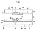
- the display device including the MEMS according to the present exemplary embodiment has a similar configuration and effect as the exemplary embodiment shown in FIG. 10 , but the reflective layer 120 including the aperture 125 is covered by a porous transparent layer 130 b .
- the effect and characteristics of the porous transparent layer 130 b are similar to those of the exemplary embodiment shown in FIG. 5 and FIG. 9 .
- FIG. 14 a method for manufacturing a display device including a MEMS having a porous transparent body or a porous transparent layer of FIG. 5 , FIG. 9 , FIG. 11 , and FIG. 13 will be described with reference to FIG. 14 , FIG. 15 , and FIG. 16 .
Landscapes
- Physics & Mathematics (AREA)
- General Physics & Mathematics (AREA)
- Optics & Photonics (AREA)
- Mechanical Light Control Or Optical Switches (AREA)
- Devices For Indicating Variable Information By Combining Individual Elements (AREA)
Abstract
Description
Claims (22)
Applications Claiming Priority (2)
| Application Number | Priority Date | Filing Date | Title |
|---|---|---|---|
| KR10-2009-0106622 | 2009-11-05 | ||
| KR1020090106622A KR101614463B1 (en) | 2009-11-05 | 2009-11-05 | Display device using mems element and manufacturing method thereof |
Publications (2)
| Publication Number | Publication Date |
|---|---|
| US20110102876A1 US20110102876A1 (en) | 2011-05-05 |
| US8027078B2 true US8027078B2 (en) | 2011-09-27 |
Family
ID=43925164
Family Applications (1)
| Application Number | Title | Priority Date | Filing Date |
|---|---|---|---|
| US12/765,326 Expired - Fee Related US8027078B2 (en) | 2009-11-05 | 2010-04-22 | Display device using MEMS element and manufacturing method thereof |
Country Status (2)
| Country | Link |
|---|---|
| US (1) | US8027078B2 (en) |
| KR (1) | KR101614463B1 (en) |
Cited By (1)
| Publication number | Priority date | Publication date | Assignee | Title |
|---|---|---|---|---|
| US9134529B2 (en) | 2011-07-21 | 2015-09-15 | Pixronix, Inc. | Display device with tapered light reflecting layer and manufacturing method for same |
Families Citing this family (9)
| Publication number | Priority date | Publication date | Assignee | Title |
|---|---|---|---|---|
| JP5808944B2 (en) | 2011-05-11 | 2015-11-10 | ピクストロニクス,インコーポレイテッド | Display device and manufacturing method of display device |
| JP5856758B2 (en) * | 2011-05-23 | 2016-02-10 | ピクストロニクス,インコーポレイテッド | Display device and manufacturing method thereof |
| KR20130072847A (en) | 2011-12-22 | 2013-07-02 | 삼성디스플레이 주식회사 | Display apparatus and fabrication method of the same |
| US20140268274A1 (en) * | 2013-03-15 | 2014-09-18 | Pixtronix, Inc. | Display Apparatus Incorporating an Elevated Aperture Layer and Methods of Manufacturing the Same |
| US20140268273A1 (en) * | 2013-03-15 | 2014-09-18 | Pixtronix, Inc. | Integrated elevated aperture layer and display apparatus |
| US9897796B2 (en) | 2014-04-18 | 2018-02-20 | Snaptrack, Inc. | Encapsulated spacers for electromechanical systems display apparatus |
| US20160202469A1 (en) * | 2015-01-14 | 2016-07-14 | Pixtronix, Inc. | Shutter-based light modulators incorporating light spreading structures |
| US20170084248A1 (en) * | 2015-09-22 | 2017-03-23 | Pixtronix, Inc. | Systems and methods for improving angular distribution of light and total light throughput in a display device |
| KR102749620B1 (en) | 2016-10-18 | 2025-01-06 | 삼성디스플레이 주식회사 | Display apparatus |
Citations (14)
| Publication number | Priority date | Publication date | Assignee | Title |
|---|---|---|---|---|
| KR19980076675A (en) | 1997-04-11 | 1998-11-16 | 박원훈 | High quality reflective holographic optical element manufacturing device |
| KR20010100566A (en) | 2000-05-03 | 2001-11-14 | 구본준, 론 위라하디락사 | Transparent Type Display Device Using Micro Electro-mechanical System |
| JP2003202567A (en) | 2001-12-29 | 2003-07-18 | Korea Inst Of Science & Technology | Three-dimensional MEMS light collector, manufacturing method thereof, and liquid crystal display device |
| KR20040058240A (en) | 2001-11-21 | 2004-07-03 | 옵티칼코팅라보라토리,인코포레이티드 | Glass panel with barrier coating and related methods |
| JP2005275061A (en) | 2004-03-25 | 2005-10-06 | Sony Corp | Hologram recording / reproducing apparatus and installation method of hologram recording medium |
| KR20060004590A (en) | 2004-07-09 | 2006-01-12 | 프라임 뷰 인터내셔널 코오포레이션 리미티드 | Structure of micro electromechanical system |
| US20060066805A1 (en) | 2004-09-30 | 2006-03-30 | Anders Grunnet-Jepsen | Liquid crystal on silicon (LCOS) microdisplay with retarder that reduces light beam polarization changes |
| KR20060116102A (en) | 2005-05-09 | 2006-11-14 | 삼성전자주식회사 | Backlight Assembly and Display Device Having Same |
| KR20060118179A (en) | 2005-05-16 | 2006-11-23 | 주식회사 하이닉스반도체 | Micro pump and its manufacturing method |
| KR20070057192A (en) | 2004-09-27 | 2007-06-04 | 아이디씨 엘엘씨 | Micromechanical system instruments with deformable membranes characterized by mechanical sustainability |
| KR20070114161A (en) | 2005-02-23 | 2007-11-29 | 픽스트로닉스 인코포레이티드 | Methods and apparatuses for operating displays |
| KR20080037072A (en) | 2005-02-23 | 2008-04-29 | 픽스트로닉스 인코포레이티드 | Display Methods and Devices |
| US7675665B2 (en) * | 2005-02-23 | 2010-03-09 | Pixtronix, Incorporated | Methods and apparatus for actuating displays |
| US7706073B2 (en) * | 2005-06-29 | 2010-04-27 | Reflexite Corporation | Collimating microlens array |
Family Cites Families (1)
| Publication number | Priority date | Publication date | Assignee | Title |
|---|---|---|---|---|
| US9158106B2 (en) * | 2005-02-23 | 2015-10-13 | Pixtronix, Inc. | Display methods and apparatus |
-
2009
- 2009-11-05 KR KR1020090106622A patent/KR101614463B1/en not_active Expired - Fee Related
-
2010
- 2010-04-22 US US12/765,326 patent/US8027078B2/en not_active Expired - Fee Related
Patent Citations (14)
| Publication number | Priority date | Publication date | Assignee | Title |
|---|---|---|---|---|
| KR19980076675A (en) | 1997-04-11 | 1998-11-16 | 박원훈 | High quality reflective holographic optical element manufacturing device |
| KR20010100566A (en) | 2000-05-03 | 2001-11-14 | 구본준, 론 위라하디락사 | Transparent Type Display Device Using Micro Electro-mechanical System |
| KR20040058240A (en) | 2001-11-21 | 2004-07-03 | 옵티칼코팅라보라토리,인코포레이티드 | Glass panel with barrier coating and related methods |
| JP2003202567A (en) | 2001-12-29 | 2003-07-18 | Korea Inst Of Science & Technology | Three-dimensional MEMS light collector, manufacturing method thereof, and liquid crystal display device |
| JP2005275061A (en) | 2004-03-25 | 2005-10-06 | Sony Corp | Hologram recording / reproducing apparatus and installation method of hologram recording medium |
| KR20060004590A (en) | 2004-07-09 | 2006-01-12 | 프라임 뷰 인터내셔널 코오포레이션 리미티드 | Structure of micro electromechanical system |
| KR20070057192A (en) | 2004-09-27 | 2007-06-04 | 아이디씨 엘엘씨 | Micromechanical system instruments with deformable membranes characterized by mechanical sustainability |
| US20060066805A1 (en) | 2004-09-30 | 2006-03-30 | Anders Grunnet-Jepsen | Liquid crystal on silicon (LCOS) microdisplay with retarder that reduces light beam polarization changes |
| KR20070114161A (en) | 2005-02-23 | 2007-11-29 | 픽스트로닉스 인코포레이티드 | Methods and apparatuses for operating displays |
| KR20080037072A (en) | 2005-02-23 | 2008-04-29 | 픽스트로닉스 인코포레이티드 | Display Methods and Devices |
| US7675665B2 (en) * | 2005-02-23 | 2010-03-09 | Pixtronix, Incorporated | Methods and apparatus for actuating displays |
| KR20060116102A (en) | 2005-05-09 | 2006-11-14 | 삼성전자주식회사 | Backlight Assembly and Display Device Having Same |
| KR20060118179A (en) | 2005-05-16 | 2006-11-23 | 주식회사 하이닉스반도체 | Micro pump and its manufacturing method |
| US7706073B2 (en) * | 2005-06-29 | 2010-04-27 | Reflexite Corporation | Collimating microlens array |
Cited By (1)
| Publication number | Priority date | Publication date | Assignee | Title |
|---|---|---|---|---|
| US9134529B2 (en) | 2011-07-21 | 2015-09-15 | Pixronix, Inc. | Display device with tapered light reflecting layer and manufacturing method for same |
Also Published As
| Publication number | Publication date |
|---|---|
| KR20110049557A (en) | 2011-05-12 |
| KR101614463B1 (en) | 2016-04-22 |
| US20110102876A1 (en) | 2011-05-05 |
Similar Documents
| Publication | Publication Date | Title |
|---|---|---|
| US8027078B2 (en) | Display device using MEMS element and manufacturing method thereof | |
| US11163195B2 (en) | Display device using a color conversion layer to display colors | |
| US8068266B2 (en) | Display substrate, method of manufacturing the same and electrowetting display panel having the display substrate | |
| US8390770B2 (en) | Liquid crystal display, color filter substrate and manufacturing method thereof | |
| KR20070010472A (en) | Hybrid polarizer, manufacturing method thereof and display device having same | |
| JP2005234515A (en) | Micro electrode mechanical system display cell and method for fabricating thereof | |
| TWI464507B (en) | Active matrix substrate and display device | |
| US12114535B2 (en) | Counter substrate, display panel, and display apparatus | |
| CN101813825A (en) | Interference light modulator and display apparatus | |
| TWI823910B (en) | Display apparatus and manufacturing method thereof | |
| JP2002014211A (en) | Reflection plate, reflection type liquid crystal display device and manufacturing method thereof, optical member, display device, illumination device, display plate, and wave member | |
| JP2005275102A (en) | Transflective liquid crystal display device and manufacturing method thereof | |
| JP2014089231A (en) | Microlens array substrate, electro-optical device, optical unit, and projector | |
| CN110320702A (en) | Substrate and preparation method thereof, display panel | |
| CN100430758C (en) | Color filter and manufacturing method thereof | |
| TWI250330B (en) | Manufacturing method of electro-optical device substrate and manufacturing method of electro-optical device | |
| JP2006509240A (en) | High refractive index coated light control film | |
| WO2004112434A1 (en) | El device, process for manufacturing the same, and liquid crystal display employing el device | |
| KR101702107B1 (en) | Display device using mems element and manufacturing method thereof | |
| CN105164565A (en) | Display device | |
| KR102286886B1 (en) | Photo mask and method of manufacturing the same | |
| JP5269861B2 (en) | Liquid crystal display | |
| WO2023173306A1 (en) | Display substrate and display apparatus | |
| CN117643195B (en) | Display panel and display device | |
| JP2002098955A (en) | Liquid crystal display device and method of manufacturing the same |
Legal Events
| Date | Code | Title | Description |
|---|---|---|---|
| AS | Assignment |
Owner name: SAMSUNG ELECTRONICS CO., LTD., KOREA, REPUBLIC OF Free format text: ASSIGNMENT OF ASSIGNORS INTEREST;ASSIGNORS:CHO, HYUN-MIN;KIM, SUNG-JIN;KIM, YU-KWAN;AND OTHERS;REEL/FRAME:024371/0416 Effective date: 20100421 |
|
| ZAAA | Notice of allowance and fees due |
Free format text: ORIGINAL CODE: NOA |
|
| ZAAB | Notice of allowance mailed |
Free format text: ORIGINAL CODE: MN/=. |
|
| STCF | Information on status: patent grant |
Free format text: PATENTED CASE |
|
| FEPP | Fee payment procedure |
Free format text: PAYOR NUMBER ASSIGNED (ORIGINAL EVENT CODE: ASPN); ENTITY STATUS OF PATENT OWNER: LARGE ENTITY |
|
| AS | Assignment |
Owner name: SAMSUNG DISPLAY CO., LTD., KOREA, REPUBLIC OF Free format text: CHANGE OF NAME;ASSIGNOR:SAMSUNG ELECTRONICS CO., LTD.;REEL/FRAME:028859/0868 Effective date: 20120403 |
|
| FPAY | Fee payment |
Year of fee payment: 4 |
|
| MAFP | Maintenance fee payment |
Free format text: PAYMENT OF MAINTENANCE FEE, 8TH YEAR, LARGE ENTITY (ORIGINAL EVENT CODE: M1552); ENTITY STATUS OF PATENT OWNER: LARGE ENTITY Year of fee payment: 8 |
|
| FEPP | Fee payment procedure |
Free format text: MAINTENANCE FEE REMINDER MAILED (ORIGINAL EVENT CODE: REM.); ENTITY STATUS OF PATENT OWNER: LARGE ENTITY |
|
| LAPS | Lapse for failure to pay maintenance fees |
Free format text: PATENT EXPIRED FOR FAILURE TO PAY MAINTENANCE FEES (ORIGINAL EVENT CODE: EXP.); ENTITY STATUS OF PATENT OWNER: LARGE ENTITY |
|
| STCH | Information on status: patent discontinuation |
Free format text: PATENT EXPIRED DUE TO NONPAYMENT OF MAINTENANCE FEES UNDER 37 CFR 1.362 |
|
| FP | Lapsed due to failure to pay maintenance fee |
Effective date: 20230927 |