US8005435B2 - Ultra-wideband transceiver - Google Patents
Ultra-wideband transceiver Download PDFInfo
- Publication number
- US8005435B2 US8005435B2 US11/799,065 US79906507A US8005435B2 US 8005435 B2 US8005435 B2 US 8005435B2 US 79906507 A US79906507 A US 79906507A US 8005435 B2 US8005435 B2 US 8005435B2
- Authority
- US
- United States
- Prior art keywords
- signal
- frequency
- baseband
- band
- low
- Prior art date
- Legal status (The legal status is an assumption and is not a legal conclusion. Google has not performed a legal analysis and makes no representation as to the accuracy of the status listed.)
- Expired - Fee Related, expires
Links
Images


Classifications
-
- H—ELECTRICITY
- H04—ELECTRIC COMMUNICATION TECHNIQUE
- H04L—TRANSMISSION OF DIGITAL INFORMATION, e.g. TELEGRAPHIC COMMUNICATION
- H04L27/00—Modulated-carrier systems
- H04L27/0008—Modulated-carrier systems arrangements for allowing a transmitter or receiver to use more than one type of modulation
-
- H—ELECTRICITY
- H04—ELECTRIC COMMUNICATION TECHNIQUE
- H04L—TRANSMISSION OF DIGITAL INFORMATION, e.g. TELEGRAPHIC COMMUNICATION
- H04L27/00—Modulated-carrier systems
- H04L27/26—Systems using multi-frequency codes
- H04L27/2601—Multicarrier modulation systems
- H04L27/2647—Arrangements specific to the receiver only
Definitions
- the present invention relates, in general, to radio frequency (RF) signal devices, and, more particularly, to ultra-wideband transceivers.
- RF radio frequency
- Wideband digital communications systems continue to increase in number and reach.
- Such systems including the various digital subscriber lines (XDSL) (e.g., asynchronous, synchronous, very high speed), IEEE 802.11 a/g Wi-Fi Wireless local area networks (LAN), IEEE 802.16 WiMAX mobile area network (MAN), IEEE 801.20 Mobile Broadband Wireless Access (MBWA), and other wide and ultra wideband (UWB) communication systems, are being established in an effort to increase the accessibility of information and communication.
- XDSL digital subscriber lines
- LAN local area networks
- MAN IEEE 802.16 WiMAX mobile area network
- MBWA Mobile Broadband Wireless Access
- UWB ultra wideband
- Single-carrier modulation schemes have generally been preferred in such systems as the single-carrier schemes tend to exhibit a higher data rate than multi-carrier schemes.
- One modulation scheme that has recently been considered for use in UWB systems is orthogonal frequency division multiplexing (OFDM).
- OFDM is a digital, multi-carrier modulation scheme that uses a large number of closely-spaced orthogonal sub-carriers, each modulated with a conventional modulation scheme, such as quadrature amplitude modulation (QAM), at a low symbol rate.
- QAM quadrature amplitude modulation
- This combination has generally produced data rates on par with conventional single-carrier schemes.
- One of the primary advantages of OFDM over single-carrier schemes, however, is the ability to deal with severe channel conditions, such as multipath and narrowband interference, without the necessity for complex equalization filters.
- Channel equalization is simplified because OFDM may be viewed as using many slowly-modulated narrowband signals rather than one rapidly-modulated wideband signal.
- Multiband OFDM is one of the modulation schemes being supported and used in digital UWB communications systems, including wireless personal area network (WPAN) technology.
- WPAN wireless personal area network
- One of the challenges in providing MB-OFDM to digital communications systems is the design and development of MB-OFDM UWB transceivers. Because the sub-carriers in MB-OFDM are orthogonal, cross-talk between the sub-channels is essentially eliminated. Thus, inter-carrier guard bands are not typically required. This feature greatly simplifies the design of the transmitters, receivers, and transceivers. However, MB-OFDM typically encourages very accurate frequency synchronization between the receiver and transmitter.
- OFDM orthogonality of the sub-carriers and cause inter-carrier interference (ICI).
- OFDM is generally susceptible to Doppler shift during movement. Therefore, the compensation for Doppler shift and other factors that affect the orthogonality of the sub-carriers increase the complexity of the transmitters, receivers, and transceivers.
- UWB transmission regulations request that the RF signal be transmitted within band groups.
- the multi-band systems divide the UWB spectrum into several smaller bands with some systems grouping those bands into band groups.
- WIMEDIA® standard which is the de facto standard radio platform for UWB wireless networking, divides the UWB spectrum into 14 bands (labeled as band # 1 -# 14 ) organized into five band groups (labeled band group (or “BG”) # 1 -# 5 ) over a center frequency range from 3432 MHz to 10296 MHz.
- the RF carrier quickly hops between each band within a particular band group.
- Two circuit architectures have been commonly deployed for MB-OFDM UWB transceivers. The first uses three different phase-locked loops (PLLs) operating at three different frequencies. The particular reference frequency is selected using an RF switch that selects the particular PLL.
- PLLs phase-locked loops
- PLLs occupy a considerable amount of chip/silicon space and consume relatively large amounts of power. Additionally, if the PLLs are not properly isolated from one another, each will introduce interference with the others.
- the RF switch also causes potential problems by introducing a different load impedance to the PLLs, which tends to disturb the lock status of the PLLs. This disturbed lock status typically calls for the addition of PLL output buffers that consume even more power and take up additional chip space.
- the second transceiver architecture deploys a single PLL at a center frequency along with a complex frequency translation circuit that either shifts the PLL output frequency up or down by a certain amount or does not shift the frequency at all. Each state depends on which frequency band is needed.
- This architecture reduces the circuit chip area and also the power consumption compared with the three-PLL transceiver.
- the output of this transceiver contains certain inevitable harmonics with amplitudes between ⁇ 30- ⁇ 50 dBc, compared with typical harmonic amplitudes between ⁇ 60- ⁇ 70 dBc in WLAN or Global System for Mobile Communications (GSM) synthesizer output.
- GSM Global System for Mobile Communications
- the higher spurious signals in the LO spectrum renders the receiver more susceptible to interference from external signals, such as those from WLAN in the 2.4-5 GHz band as well as the future signals from WiMAX in the >3.5 GHz band.
- Such high power interference signals are 40-50 dB higher than UWB signals to begin with, and when mixed into the MB-OFDM baseband spectrum, would likely disable normal operation of a UWB system without extra RF filtering.
- EMI electromagnetic interference
- the zero-IF processing section is preferably made from a combination of linear elements, such as amplifiers, filters, as well as single side-band (SSB) frequency converters, and analog switches.
- SSB single side-band
- a method for processing one or more information signals includes receiving a broadcast radio frequency (RF) signal that represents one of the information signals.
- the broadcast RF signal is translated into a low-frequency intermediate frequency (IF) signal using a reference signal provided by a phase-locked loop (PLL).
- the PLL is configured to selectively provide a reference signal at one of a plurality of frequencies representing a center frequency for a plurality of signal band groups.
- the low-frequency IF signal is selectively modulated into a baseband information signal, which is then digitized into a digital information signal.
- another digital information signal is designated for transmission.
- This digital information signal is converted into an analog baseband signal and then selectively converted into another low-frequency IF signal.
- the low-frequency IF signal is selectively modulated into a transmission RF signal.
- the transmission RF signal may then be transmitted or broadcast.
- an ultra wideband (UWB) communication component includes a digital-to-analog converter (DAC) operable to convert input digital data into a baseband analog signal.
- the component also includes a selective intermediate frequency (IF) component configured to selectively generate a low-frequency IF signal from the baseband analog signal. The selective generation is based on a target signal band in one of the signal band groups.
- the component also includes a phase-locked loop (PLL) adapted to selectively produce a reference signal at one of a plurality of center frequencies associated with the plurality of signal band groups.
- a radio frequency (RF) modulator is also included that is configured to use the reference signal to modulate the low-frequency IF signal into an RF transmission signal of the target signal band.
- a method for processing ultra wideband (UWB) information signals in a receiver path includes receiving an RF information signal that has a frequency within one of a plurality of signal band groups. Responsive to that particular frequency, a reference signal is selected from a plurality of frequencies that represent a center frequency for the plurality of signal band groups. The RF information signal is mixed into a zero IF signal using the selected reference signal and selectively converted into a baseband signal. The baseband signal is then digitized into a digital information signal for presentation.
- UWB ultra wideband
- an ultra wideband (UWB) transceiver includes a receiver path and a transmitter path.
- the transmitter path includes a digital-to-analog converter (DAC) operable to convert input digital data into a baseband analog signal. It also includes a selective intermediate frequency (IF) component configured to selectively generate a low-frequency IF signal from the baseband analog signal. Selection is based on a target signal band in one of the signal band groups.
- DAC digital-to-analog converter
- IF intermediate frequency
- the UWB transceiver includes a phase-locked loop (PLL) adapted to selectively produce a reference signal at one of a plurality of center frequencies associated with the plurality of signal band groups, and also includes a radio frequency (RF) modulator configured to use the reference signal to modulate the low-frequency IF signal into an RF transmission frequency of the target signal band.
- the receiver path includes a mixer configured to use a receiver reference signal from the same PLL to translate a received RF data signal into another low-frequency IF signal.
- There is also a selective IF receiver component configured to selectively generate another baseband analog signal. The selection of the baseband frequency generation is based on an originating signal band in one of the plurality of signal band groups.
- the receiver path also includes an analog-to-digital converter (ADC) operable to convert the baseband analog signal into a digital information signal that is then used for presentation of the information.
- ADC analog-to-digital converter
- One advantage of the various embodiments of the present invention is that the ultra-fast-hopping RF synthesizer of the prior art is now replaced with the complexity of the UWB IF section, which is either linear or, under current regulations, has a fixed frequency of around 524 MHz.
- the power and area requirements for implementing such an UWB IF section are much less (lower power and lower chip area) and fabrication is much easier than implementing the ultra-fast-hopping RF synthesizer of the prior art.
- LO local oscillator
- FIG. 1 is a block circuit diagram of a receiver path of a MB-OFDM transceiver configured according to one embodiment of the present invention
- FIG. 2 is a graph illustrating zero-IF signals generated in a transceiver configured according to one embodiment of the present invention
- FIG. 3 is a circuit diagram illustrating wideband RX-IF circuitry configured according to one embodiment of the present invention
- FIG. 4 is a circuit diagram illustrating the transmission path of a MB-OFDM transceiver configured according to one embodiment of the present invention
- FIG. 5 is a circuit diagram illustrating wideband TX-IF circuitry in a MB-OFDM transceiver configured according to one embodiment of the present invention
- FIG. 6 is a block diagram illustrating a MB-OFDM transceiver configured according to one embodiment of the present invention
- FIG. 7 is a flowchart illustrating example steps executed when operating a UWB transceiver configured according to one embodiment of the present invention
- FIG. 8 is a flowchart illustrating example steps executed in the receiver process step illustrated in FIG. 7 ;
- FIG. 9 is a flowchart illustrating example steps executed in the transmission process step illustrated in FIG. 7 .
- Receiver path 10 comprises three path sections: (1) RF section 100 ; (2) intermediate frequency (IF) section 108 ; and (3) analog-to-digital conversion (ADC) section 109 . Each section will be described in detail below.
- RF section 100 comprises low noise amplifier 101 connected to mixers 102 and 103 .
- Mixers 102 and 103 are provided with a reference signal generated by PLL 105 .
- the reference signal from PLL 105 enters mixer 102 directly, but the reference signal that enters mixer 103 first passes through phase shifter 106 , in which the reference signal is shifted by 90° to create the quadrature of the reference signal.
- RF section 100 therefore, provides an I/Q signal output consisting of information signal (I IF ) and quadrature signal (Q IF ).
- I IF and Q IF are then conditioned before exiting RF section 100 by passing through low-pass filters (LPF) 104 and 107 , respectively.
- LPF low-pass filters
- the input signals to RF section 100 is represented by two formulae: A cos( ⁇ o ⁇ i )t (1) +B cos( ⁇ o ⁇ i )t (2)
- a and B are time varying functions slower than radio frequency ⁇ o or intermediate frequency ⁇ i .
- the sign used in equations (1) and (2) depends on whether the signals originate from the upper band, which uses +, or the lower band, which uses ⁇ .
- the input signals are conditioned and amplified by LNA 101 and split into two paths.
- the first path provides a first input to mixer 102 .
- the reference input to mixer 102 is provided by PLL 105 .
- the frequency of the reference input generated by PLL 105 will depend on which band group the receiver is receiving from.
- the reference input signal generated by PLL 105 is represented by the formula: cos ⁇ o t (3)
- the second path from LNA 101 provides a first input to mixer 103 .
- the reference signal generated by PLL 105 is first phase-shifted by 90° before arriving at mixer 103 as a quadrature (Q) reference signal.
- I IF A cos( ⁇ o ⁇ i ) t cos ⁇ o t ⁇ A/ 2 cos ⁇ i t (5)
- I IF +B cos ( ⁇ o ⁇ i ) t cos ⁇ o t ⁇ B/ 2 sin ⁇ i t (6)
- the sign of the resulting signal depends on whether the signal originates from the upper band, in which the sign for the A signal will be +, with the sign for the upper band B signal being ⁇ , or the lower band, in which the sign for A will be ⁇ , with the sign for the lower band B being +.
- the resulting mixed signals, Q IF , output from mixer 103 are represented by the following formula:
- Q IF A cos( ⁇ o ⁇ i ) t sin ⁇ o t ⁇ A/ 2 sin ⁇ i t (7)
- Q IF +B cos( ⁇ o ⁇ i ) t sin ⁇ o t ⁇ B/ 2 cos ⁇ i t (8)
- I IF and Q IF are then filtered at LPF 104 and 107 to remove any unwanted and/or spurious signals above a desired frequency.
- mixers 102 and 103 are designed along with the reference signals from PLL 105 to generate an IF signal having a very low frequency, i.e., lower than about 800 MHz. IF signals in this frequency range are typically referred to as zero-IF signals.
- the zero-IF approach enables direct conversion of analog RF signals to a digital baseband format, which allows for a reduction in the necessary hardware components.
- the UWB transceiver operates according to the WIMAX® standard.
- PLL 105 is capable of generating the center frequency for each band group (i.e., 3960 MHz—BG # 1 ; 5544 MHz—BG # 2 ; 7128 MHz—BG # 3 ; etc.).
- LPF 104 and 107 have a cut-off frequency about 792 MHz or so.
- IF section 108 comprises wideband RX-IF circuitry 30 (detailed in FIG. 3 ), which processes I IF and Q IF into baseband signals I BB and Q BB .
- I BB and Q BB are then input into ADC section 109 , in which I BB is converted into a digital signal by ADC 110 and Q BB is converted into a digital signal by ADC 111 .
- I DCT and Q DCT are output from receiver section 10 of the UWB transceiver for further desired processing of the transmitted information.
- FIG. 2 a graph illustrates zero-IF signals generated in a transceiver configured according to one embodiment of the present invention.
- the zero-IF signals represent the three signal bands of an entire band group.
- the zero-IF signals illustrated in graph 20 represent the signal bands of WIMAX® band group # 1 , band # 1 — 200 , band # 2 — 201 , and band # 3 — 202 , after being processed by a low-pass filter, such as LPF 104 or 107 ( FIG. 1 ), to remove any unnecessary spurious signals.
- a low-pass filter such as LPF 104 or 107
- bands # 1 — 200 , # 2 — 201 , and # 3 — 202 would take turns, such that, at any given transmission point, only one such signal band would be present in the zero-IF signal. All three signal bands are illustrated in graph 20 of FIG. 2 to provide a representation of the wideband signal of the entire band group.
- FIG. 3 is a circuit diagram illustrating wideband RX-IF circuitry 30 configured according to one embodiment of the present invention.
- Zero-IF signals, I IF and Q IF enter wideband RX-IF circuitry 30 at inputs 300 and 301 to be converted into baseband signals.
- the path that each signal takes through wideband RX-IF circuitry 30 depends on which of the signal bands is received.
- the center IF frequency, ⁇ i equals about 524 MHz
- the signal corresponds to the upper band signal, i.e., signal band # 3 — 202 ( FIG. 2 ) and is processed through the mixing circuits of wideband RX-IF circuitry 30 .
- the signal corresponds to the middle band signal, i.e., signal band # 2 — 201 ( FIG. 2 ) and is sent directly through wideband RX-IF circuitry 30 without any further processing.
- I IF will be output directly as I BB
- Q IF will be output directly as Q BB .
- the center IF frequency ⁇ i equals about ⁇ 524 MHz
- the signal corresponds to the lower band signal, i.e., signal band # 1 — 200 ( FIG. 2 ) and is, once again, processed through the mixing circuits of wideband RX-IF circuitry 30 .
- Switches 307 - 310 control which signals are output at I BB output 314 and Q BB output 315 .
- Switches 307 and 309 are closed and switches 308 and 310 are open when the center IF frequency, ⁇ i , equals about 0 Hz. This provides a completed circuit straight through wideband RX-IF circuitry 30 to I BB output 314 and Q BB output 315 .
- Switches 308 and 310 are closed and switches 307 and 309 are open when the center IF frequency, ⁇ i , does not equal about 0 Hz.
- This switch set-up provides the circuit path through the various mixing stages of wideband RX-IF circuitry 30 .
- the output at I BB output 314 and Q BB output 315 is controlled by the frequency of ⁇ i .
- Wideband RX-IF circuitry 30 also includes mixers 302 and 303 , which operate on I T .
- Mixer 302 processes I IF with a first reference signal from IF PLL 305 to output I 2 IF .
- Mixer 303 processes I IF with a quadrature reference signal, which results from the first reference signal from IF PLL 305 being shifted in phase by 90° by phase shifter 304 .
- Mixer 303 outputs IQ IF .
- Mixers 311 and 312 are also included in wideband RX-IF circuitry 30 for processing Q IF .
- Mixer 312 mixes Q IF with the first reference signal from IF PLL 305 to output QI IF .
- Mixer 311 mixes Q IF with the quadrature reference signal from IF PLL 305 to output Q 2 IF .
- the baseband output signals, I BB and Q BB are then generated from I 2 IF , IQ IF , QI IF , and Q 2 IF , respectively.
- I BB is formed by adding or subtracting I 2 IF and Q 2 IF
- Q BB is formed by adding or subtracting QI IF and IQ IF .
- the determination of whether the respective mixed signals are added or subtracted depends on whether or not the initial signal originates in the upper band or the lower band.
- the upper band signals are mixed to signal band # 1 — 200 . Because the desired baseband frequency is the frequency represented by signal band # 2 — 201 , when the upper band is determined, the upper band IF signal will be translated up to the frequency of signal band # 2 — 201 . Conversely, the lower band signals mix to signal band # 3 — 202 .
- the lower band signals are translated lower by the same amount (about 524 MHz in FIG. 2 ), to reach the appropriate baseband frequency. Because the middle band signals mix to the desired baseband frequency, no further mixing of modulating is required, and the mixed middle band signals are passed directly on to become the baseband signal.
- FIG. 4 is a circuit diagram illustrating transmission path 40 of an MB-OFDM transceiver configured according to one embodiment of the present invention.
- Transmission path 40 comprises digital-to-analog conversion (DAC) section 410 , transmission (TX) IF section 411 , and RF section 412 .
- Digital information is received in quadrature at inputs 400 and 401 , converted to analog and processed before transmission through PA modulator 409 .
- I DCT and Q DCT Digital input signals, enter transmission path 40 through inputs 400 and 401 .
- I DCT is processed by DAC 402 converting the digital signal into analog baseband signal, I BB .
- Q DCT is similarly processed by DAC 403 converting the digital signal into analog baseband quadrature signal, Q BB .
- I BB and Q BB then enter wideband TX-IF circuitry 50 of TX-IF section 411 for conversion from baseband to IF.
- I BB and Q BB originate in the middle band, they are directly amplified into I IF and Q IF without any frequency translation.
- I BB and Q BB are in the upper or lower bands, they are translated by around +528 MHz, for upper band, and about ⁇ 528 MHz, for lower band, into I IF and Q IF .
- I IF and Q IF exit TX-IF section 412 and enter RF section 412 through LPF 404 and 405 .
- LPF 404 and 405 each have a cutoff frequency of about 792 MHz, thus, passing I IF and Q IF with any unwanted spurious signals cut off over that frequency.
- I IF and Q IF are mixed into RF transmission frequency through mixers 406 and 407 .
- PLL 105 which is shared with receiver path 10 ( FIG. 1 ), provides the reference signals for translating I IF and Q IF to the appropriate transmission frequencies. As noted before, PLL 105 is capable of generating the center frequency for each band group. Therefore, the reference signal generated by PLL 105 is controlled by the target band group for the information signals, I IF and Q IF .
- Mixer 406 translates I IF into I RF using the reference signal provided by PLL 105 .
- Mixer 407 translates Q IF also into I RF using the quadrature reference signal resulting from the reference signal from PLL 105 being phase shifted by 90° in phase shifter 408 .
- the two results of mixing Q IF with the quadrature reference signal shifts the quadrature signal back in phase with I RF .
- I RF is then input into PA 409 for amplification and modulation for ultimate transmission.
- FIG. 5 is a circuit diagram illustrating wideband TX-IF circuitry 50 in an MB-OFDM transceiver configured according to one embodiment of the present invention.
- the input signals, I BB and Q BB , from DAC section 410 ( FIG. 4 ) are processed in wideband TX-IF circuitry 50 according to which signal band the signal is targeted for.
- switches 510 and 512 close, allowing I BB and Q BB to pass directly to outputs 514 and 515 as IF signals, I IF and Q IF .
- switches 510 and 512 remain open, while switches 511 and 513 close, allowing I BB and Q BB to be modulated by an IF carrier frequency around ⁇ 524 MHz (+ for the upper band and ⁇ for the lower band).
- I BB is processed through mixers 502 and 503 .
- IF PLL 506 provides a reference signal to mixer 502 in modulating I BB to I 2 BB .
- IF PLL 506 also provides the reference signal to mixer 503 , but its reference signal is shifted by 90° in phase shifter 507 .
- the resulting quadrature reference signal is mixed with I BB at mixer 503 to produce IQ BB .
- Q BB is processed through mixers 504 and 505 .
- IF PLL 506 provides the same reference signal and quadrature reference signal to mixers 504 and 505 , respectively.
- Q BB is, therefore, modulated with the reference signal to result in QI BB while it is modulated with the quadrature reference signal to result in Q 2 BB .
- I 2 BB is combined with Q 2 BB to generate I IF
- IQ BB is combined with QI BB to generate Q IF .
- the selections of whether or not to modulate the baseband signal into the corresponding zero IF signal are determined much like the selections in the receiver path discussed above.
- the baseband signals are translated either up (upper band) or down (lower band) to equal the desired zero IF signal frequency, represented by signal band # 2 — 201 ( FIG. 2 ). Otherwise, because the resulting baseband signal targeted for the middle band arrives at the desired signal band # 2 — 201 ( FIG. 2 ) bandwidth, it is passed directly on through to the zero IF signal.
- FIG. 6 is a block diagram illustrating MB-OFDM transceiver 601 configured according to one embodiment of the present invention.
- UWB digital communication system 60 includes interface 602 connected to transceiver 601 .
- the information signals 603 and 604 are transmitted and received through antenna 600 .
- UWB digital communication system 60 may comprise a mobile telecommunication system.
- a user provides data, which could be audio, video, voice, data, and the like to interface 602 .
- Interface 602 operates using digital information, thus the data provided by the user exists in digital form within interface 602 .
- Transceiver 601 processes the digital data from interface 602 into analog RF data for transmission through antenna 600 as transmitted data 604 .
- the transmission functionality of transceiver 601 operates substantially according to the processes described in transmission path 40 ( FIG. 4 ).
- transceiver 601 receives broadcast information 603 from antenna 600 and processed by transceiver 601 for presentation on interface 602 .
- Transceiver 601 takes the RF broadcast information 603 , and converts it to a baseband signal and then into the digital signal that is compatible with interface 602 .
- the receiver functionality of transceiver 601 operates substantially according to the processes described in receiver path 10 ( FIG. 1 ).
- transceiver 601 would comprise the various circuit features or features similar to those illustrated and described in FIGS. 1 and 3 - 5 .
- transceiver 601 is described as comprising the similar or same circuit features described in FIGS. 1 and 3 - 5 , transceiver 601 is not limited to only those circuit elements depicted in those FIGURES. The features and functionalities of transceiver 601 may be implemented through various additional and/or alternative circuit elements.
- FIGS. 1-5 are merely exemplary parameters used for purposes of describing the features and functions of the one embodiment of the present invention.
- FIGS. 1-5 have been described in terms of a communication system configured according to the WIMEDIA® standard for UWB communication systems. Additional and/or alternative embodiments of the present invention may be used in conjunction with other types of communication systems, which may, in turn, call for the processing of signal frequencies of a different level or grouping scheme.
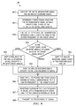
- FIG. 7 is a flowchart illustrating example steps executed when operating a UWB transceiver configured according to one embodiment of the present invention.
- a broadcast RF signal is received over an antenna.
- a digital signal directed for transmission is received at a UWB transceiver in step 702 .
- a determination is made, in step 703 , whether the signal is an RF signal (i.e., an in-coming signal), or a digital signal (i.e., an out-going signal). If the signal is an in-coming signal, the RF signal is processed, in receiver process step 80 , in a receiver path.
- RF signal i.e., an in-coming signal
- a digital signal i.e., an out-going signal
- the resulting processed RF signal is then provided to an interface in step 704 . If the signal is an out-going signal, the digital signal is processed, in transmission process step 90 , in a transmission path. The resulting processed digital signal is then transmitted over an antenna in step 705 .
- FIG. 8 is a flowchart illustrating example steps executed in receiver process step 80 , as illustrated in FIG. 7 .
- the signal band group from which the broadcast RF signal originates is determined.
- a PLL is tuned, in step 801 , to provide a reference signal that corresponds to the center frequency of the originating signal band group, the PLL configured to selectively provide a reference signal at one of a plurality of frequencies that represent the center frequency for each of the signal band groups.
- the broadcast RF signal is translated to a low-frequency IF signal using the reference signal.
- a determination is made, in step 803 , whether the frequency of the low-frequency IF signal is equal to a baseband signal.
- the low-frequency IF signal is modulated, in step 804 , by a predetermined frequency to create a baseband information signal. Otherwise, the low-frequency IF signal is set equal to the baseband information signal in step 805 . The resulting baseband information signal is then digitized into a digital information signal, in step 806 .
- FIG. 9 is a flowchart illustrating example steps executed in transmission process step 90 , as illustrated in FIG. 7 .
- the digital information signal is converted into an analog baseband signal.
- the target signal group is then determined from the plurality of signal band groups, in step 901 , as well as the target signal band within the target group.
- the PLL is then tuned, in step 902 , to provide the transmission reference signal, wherein the transmission reference signal corresponds to the center frequency of the target signal group.
- a determination is made, in step 903 whether the target signal band is an upper, middle, or lower band of the target signal group. If the target signal band is the upper band, then the analog baseband signal is shifted higher, in step 904 , by a predetermined frequency.
- the analog baseband signal is shifted lower, in step 905 , by the predetermined amount. If the target signal band is the middle band, then the analog baseband signal is passed directly to the low-frequency IF signal in step 906 .
- the PLL is then tuned again, in step 907 , to provide the transmission reference signal, wherein the transmission reference signal corresponds to the center frequency of the target signal group.
- the low-frequency IF signal is then selectively modulated into a transmission RF signal, in step 908 , using the transmission reference signal provided by the PLL.
- the transmission RF signal is transmitted in step 909 .
Landscapes
- Engineering & Computer Science (AREA)
- Signal Processing (AREA)
- Computer Networks & Wireless Communication (AREA)
- Transceivers (AREA)
Abstract
Description
A cos(ωo±ωi)t (1)
+B cos(ωo±ωi)t (2)
cos ωot (3)
cos(ωo t+90)=sin ωo t (4)
I IF =A cos(ωo±ωi)t cos ωo t→±A/2 cos ωi t (5)
I IF =+B cos (ωo±ωi)t cos ωo t→±B/2 sin ωi t (6)
Q IF =A cos(ωo±ωi)t sin ωo t→±A/2 sin ωi t (7)
Q IF =+B cos(ωo±ωi)t sin ωo t→±B/2 cos ωi t (8)
Claims (47)
Priority Applications (1)
| Application Number | Priority Date | Filing Date | Title |
|---|---|---|---|
| US11/799,065 US8005435B2 (en) | 2007-04-30 | 2007-04-30 | Ultra-wideband transceiver |
Applications Claiming Priority (1)
| Application Number | Priority Date | Filing Date | Title |
|---|---|---|---|
| US11/799,065 US8005435B2 (en) | 2007-04-30 | 2007-04-30 | Ultra-wideband transceiver |
Publications (2)
| Publication Number | Publication Date |
|---|---|
| US20080267325A1 US20080267325A1 (en) | 2008-10-30 |
| US8005435B2 true US8005435B2 (en) | 2011-08-23 |
Family
ID=39886967
Family Applications (1)
| Application Number | Title | Priority Date | Filing Date |
|---|---|---|---|
| US11/799,065 Expired - Fee Related US8005435B2 (en) | 2007-04-30 | 2007-04-30 | Ultra-wideband transceiver |
Country Status (1)
| Country | Link |
|---|---|
| US (1) | US8005435B2 (en) |
Cited By (1)
| Publication number | Priority date | Publication date | Assignee | Title |
|---|---|---|---|---|
| CN107846378A (en) * | 2016-09-19 | 2018-03-27 | 华为技术有限公司 | A kind of modulator approach, demodulation method, relevant device and system |
Families Citing this family (4)
| Publication number | Priority date | Publication date | Assignee | Title |
|---|---|---|---|---|
| US7782765B2 (en) | 2007-01-22 | 2010-08-24 | Harris Stratex Networks Operating Corporation | Distributed protection switching architecture for point-to-point microwave radio systems |
| US8095088B2 (en) | 2007-05-17 | 2012-01-10 | Harris Stratex Networks Operating Corporation | Compact wide dynamic range transmitter for point to point radio |
| US8275071B2 (en) * | 2007-05-17 | 2012-09-25 | Harris Stratex Networks Operating Corporation | Compact dual receiver architecture for point to point radio |
| US9209964B2 (en) * | 2014-02-19 | 2015-12-08 | Cornet Technology, Inc. | Systems and methods for DTE/DCE CESoP timing |
Citations (14)
| Publication number | Priority date | Publication date | Assignee | Title |
|---|---|---|---|---|
| US6501410B1 (en) * | 1999-11-19 | 2002-12-31 | Anritsu Corporation | Signal analyzing apparatus |
| US20040189326A1 (en) * | 2003-03-27 | 2004-09-30 | Agilent Technologies, Inc. | Vector-detecting apparatus and impedance measuring apparatus |
| US20040218693A1 (en) * | 1999-02-02 | 2004-11-04 | Hickling Ronald M. | Direct conversion delta-sigma receiver |
| US20060068739A1 (en) * | 2004-09-30 | 2006-03-30 | Renesas Technology Corp. | Receiver, receiving method and portable wireless apparatus |
| US20060084382A1 (en) * | 2004-11-01 | 2006-04-20 | Brima Ibrahim | Method and system for selective equalization enablement based on modulation type |
| US20070025456A1 (en) * | 2005-07-29 | 2007-02-01 | Mccrady Dennis D | Methods and apparatus for encoding information in a signal by spectral notch modulation |
| US20070096980A1 (en) * | 2005-11-03 | 2007-05-03 | Nemerix Sa | Multiband GNSS receiver |
| US20070110171A1 (en) * | 2004-10-25 | 2007-05-17 | Sony Corporation | Wireless communication device |
| US20070160164A1 (en) * | 2005-11-18 | 2007-07-12 | Sahota Gurkanwal S | Digital transmitters for wireless communication |
| US20070173277A1 (en) * | 1996-10-11 | 2007-07-26 | Yun Louid C | Power control with signal quality estimation for smart antenna communications systems |
| US20070177653A1 (en) * | 2004-07-10 | 2007-08-02 | Bjorn Bjerede | High-dynamic-range ultra wide band transceiver |
| US20070223608A1 (en) * | 2006-03-22 | 2007-09-27 | Sony Corporation | Wireless communication apparatus |
| US20070232244A1 (en) * | 2006-03-31 | 2007-10-04 | Mo Shaomin S | Method of spatial band reuse in a multi-band communication system |
| US20080266161A1 (en) * | 2007-04-30 | 2008-10-30 | Josef Zipper | Analog-to-digital converter, receiver arrangement, filter arrangement and signal processing method |
-
2007
- 2007-04-30 US US11/799,065 patent/US8005435B2/en not_active Expired - Fee Related
Patent Citations (14)
| Publication number | Priority date | Publication date | Assignee | Title |
|---|---|---|---|---|
| US20070173277A1 (en) * | 1996-10-11 | 2007-07-26 | Yun Louid C | Power control with signal quality estimation for smart antenna communications systems |
| US20040218693A1 (en) * | 1999-02-02 | 2004-11-04 | Hickling Ronald M. | Direct conversion delta-sigma receiver |
| US6501410B1 (en) * | 1999-11-19 | 2002-12-31 | Anritsu Corporation | Signal analyzing apparatus |
| US20040189326A1 (en) * | 2003-03-27 | 2004-09-30 | Agilent Technologies, Inc. | Vector-detecting apparatus and impedance measuring apparatus |
| US20070177653A1 (en) * | 2004-07-10 | 2007-08-02 | Bjorn Bjerede | High-dynamic-range ultra wide band transceiver |
| US20060068739A1 (en) * | 2004-09-30 | 2006-03-30 | Renesas Technology Corp. | Receiver, receiving method and portable wireless apparatus |
| US20070110171A1 (en) * | 2004-10-25 | 2007-05-17 | Sony Corporation | Wireless communication device |
| US20060084382A1 (en) * | 2004-11-01 | 2006-04-20 | Brima Ibrahim | Method and system for selective equalization enablement based on modulation type |
| US20070025456A1 (en) * | 2005-07-29 | 2007-02-01 | Mccrady Dennis D | Methods and apparatus for encoding information in a signal by spectral notch modulation |
| US20070096980A1 (en) * | 2005-11-03 | 2007-05-03 | Nemerix Sa | Multiband GNSS receiver |
| US20070160164A1 (en) * | 2005-11-18 | 2007-07-12 | Sahota Gurkanwal S | Digital transmitters for wireless communication |
| US20070223608A1 (en) * | 2006-03-22 | 2007-09-27 | Sony Corporation | Wireless communication apparatus |
| US20070232244A1 (en) * | 2006-03-31 | 2007-10-04 | Mo Shaomin S | Method of spatial band reuse in a multi-band communication system |
| US20080266161A1 (en) * | 2007-04-30 | 2008-10-30 | Josef Zipper | Analog-to-digital converter, receiver arrangement, filter arrangement and signal processing method |
Non-Patent Citations (2)
| Title |
|---|
| "High Rate Ultra Wideband PHY and MAC Standard" Standard ECMA-368, Ecma International, 1st Edition, Dec. 2005, 322 pages. |
| "MAC-PHY Interface Specification for ECMA-368" Standard ECMA-369, Ecma International, 1st Edition, Dec. 2005, 52 pages. |
Cited By (2)
| Publication number | Priority date | Publication date | Assignee | Title |
|---|---|---|---|---|
| CN107846378A (en) * | 2016-09-19 | 2018-03-27 | 华为技术有限公司 | A kind of modulator approach, demodulation method, relevant device and system |
| CN107846378B (en) * | 2016-09-19 | 2020-12-15 | 华为技术有限公司 | Modulation method, demodulation method, related equipment and system |
Also Published As
| Publication number | Publication date |
|---|---|
| US20080267325A1 (en) | 2008-10-30 |
Similar Documents
| Publication | Publication Date | Title |
|---|---|---|
| US6081697A (en) | Multi-carrier radio system and radio transceiver implementation | |
| EP2396890B1 (en) | Multi-band aggregated spectrum receiver employing frequency source reuse | |
| US7890078B2 (en) | Dual band WLAN communication frequency synthesizer technique | |
| WO2009131076A1 (en) | Radio communication device | |
| US6735426B1 (en) | Multiple-band wireless transceiver with quadrature conversion transmitter and receiver circuits | |
| US11031962B2 (en) | Carrier aggregated signal transmission and reception | |
| US20070155350A1 (en) | Method of frequency planning in an ultra wide band system | |
| US20040259518A1 (en) | Multi standard transceiver architecture for wlan | |
| US20100074303A1 (en) | Wireless Communication Apparatus | |
| KR101172349B1 (en) | Multi-frequency Synthesizing Apparatus and Method for Multi-band RF Receiver | |
| JP2000031861A (en) | Transceiver for radio communication | |
| US9088468B2 (en) | Double conversion dual-carrier radio frequency receiver | |
| EP2086116A2 (en) | Method and arrangement for signal processing in a receiver that can be tuned to different carriers | |
| US6754508B1 (en) | Multiple-band wireless transceiver with quadrature conversion transmitter and receiver circuits | |
| US20070155348A1 (en) | Apparatus and method for ultra wide band architectures | |
| US8005435B2 (en) | Ultra-wideband transceiver | |
| KR101044864B1 (en) | Signal generating unit and signal receiving unit | |
| KR100527844B1 (en) | High Frequency Transceiver | |
| US7268640B2 (en) | Frequency generator arrangement | |
| KR100646314B1 (en) | Multi-input multi-frequency synthesizing apparatus and method for multi-band rf receiver | |
| US20070121740A1 (en) | Selective attenuation in spectral notching | |
| TW202034638A (en) | Transmission interface, communication apparatus and method for transfering a plurality of signals | |
| TWI449348B (en) | Multi-carrier receiver, multi-carrier transmitter and multi-carrier transceiver system | |
| CN105357164B (en) | Multicarrier receiver, multicarrier transmitter and multicarrier transceiving system | |
| Lee et al. | A wimedia UWB transceiver for 4-HD channel streaming |
Legal Events
| Date | Code | Title | Description |
|---|---|---|---|
| AS | Assignment |
Owner name: TAIWAN SEMICONDUCTOR MANUFACTURING COMPANY, LTD., Free format text: ASSIGNMENT OF ASSIGNORS INTEREST;ASSIGNOR:JOU, CHEWN-PU;REEL/FRAME:019392/0004 Effective date: 20070425 |
|
| STCF | Information on status: patent grant |
Free format text: PATENTED CASE |
|
| CC | Certificate of correction | ||
| FPAY | Fee payment |
Year of fee payment: 4 |
|
| FEPP | Fee payment procedure |
Free format text: MAINTENANCE FEE REMINDER MAILED (ORIGINAL EVENT CODE: REM.); ENTITY STATUS OF PATENT OWNER: LARGE ENTITY |
|
| LAPS | Lapse for failure to pay maintenance fees |
Free format text: PATENT EXPIRED FOR FAILURE TO PAY MAINTENANCE FEES (ORIGINAL EVENT CODE: EXP.); ENTITY STATUS OF PATENT OWNER: LARGE ENTITY |
|
| STCH | Information on status: patent discontinuation |
Free format text: PATENT EXPIRED DUE TO NONPAYMENT OF MAINTENANCE FEES UNDER 37 CFR 1.362 |
|
| FP | Lapsed due to failure to pay maintenance fee |
Effective date: 20190823 |