US8001513B2 - Integrated circuit apparatus, systems, and methods - Google Patents
Integrated circuit apparatus, systems, and methods Download PDFInfo
- Publication number
- US8001513B2 US8001513B2 US12/197,869 US19786908A US8001513B2 US 8001513 B2 US8001513 B2 US 8001513B2 US 19786908 A US19786908 A US 19786908A US 8001513 B2 US8001513 B2 US 8001513B2
- Authority
- US
- United States
- Prior art keywords
- integrated circuits
- vertical stack
- electrical
- circuit
- electrical connections
- Prior art date
- Legal status (The legal status is an assumption and is not a legal conclusion. Google has not performed a legal analysis and makes no representation as to the accuracy of the status listed.)
- Active, expires
Links
Images


Classifications
-
- H—ELECTRICITY
- H01—ELECTRIC ELEMENTS
- H01L—SEMICONDUCTOR DEVICES NOT COVERED BY CLASS H10
- H01L23/00—Details of semiconductor or other solid state devices
- H01L23/48—Arrangements for conducting electric current to or from the solid state body in operation, e.g. leads, terminal arrangements ; Selection of materials therefor
-
- H—ELECTRICITY
- H01—ELECTRIC ELEMENTS
- H01L—SEMICONDUCTOR DEVICES NOT COVERED BY CLASS H10
- H01L24/00—Arrangements for connecting or disconnecting semiconductor or solid-state bodies; Methods or apparatus related thereto
- H01L24/01—Means for bonding being attached to, or being formed on, the surface to be connected, e.g. chip-to-package, die-attach, "first-level" interconnects; Manufacturing methods related thereto
- H01L24/42—Wire connectors; Manufacturing methods related thereto
- H01L24/47—Structure, shape, material or disposition of the wire connectors after the connecting process
- H01L24/49—Structure, shape, material or disposition of the wire connectors after the connecting process of a plurality of wire connectors
-
- H—ELECTRICITY
- H01—ELECTRIC ELEMENTS
- H01L—SEMICONDUCTOR DEVICES NOT COVERED BY CLASS H10
- H01L21/00—Processes or apparatus adapted for the manufacture or treatment of semiconductor or solid state devices or of parts thereof
- H01L21/02—Manufacture or treatment of semiconductor devices or of parts thereof
- H01L21/04—Manufacture or treatment of semiconductor devices or of parts thereof the devices having at least one potential-jump barrier or surface barrier, e.g. PN junction, depletion layer or carrier concentration layer
- H01L21/50—Assembly of semiconductor devices using processes or apparatus not provided for in a single one of the subgroups H01L21/06 - H01L21/326, e.g. sealing of a cap to a base of a container
-
- H—ELECTRICITY
- H01—ELECTRIC ELEMENTS
- H01L—SEMICONDUCTOR DEVICES NOT COVERED BY CLASS H10
- H01L25/00—Assemblies consisting of a plurality of individual semiconductor or other solid state devices ; Multistep manufacturing processes thereof
- H01L25/03—Assemblies consisting of a plurality of individual semiconductor or other solid state devices ; Multistep manufacturing processes thereof all the devices being of a type provided for in the same subgroup of groups H01L27/00 - H01L33/00, or in a single subclass of H10K, H10N, e.g. assemblies of rectifier diodes
- H01L25/04—Assemblies consisting of a plurality of individual semiconductor or other solid state devices ; Multistep manufacturing processes thereof all the devices being of a type provided for in the same subgroup of groups H01L27/00 - H01L33/00, or in a single subclass of H10K, H10N, e.g. assemblies of rectifier diodes the devices not having separate containers
- H01L25/065—Assemblies consisting of a plurality of individual semiconductor or other solid state devices ; Multistep manufacturing processes thereof all the devices being of a type provided for in the same subgroup of groups H01L27/00 - H01L33/00, or in a single subclass of H10K, H10N, e.g. assemblies of rectifier diodes the devices not having separate containers the devices being of a type provided for in group H01L27/00
- H01L25/0657—Stacked arrangements of devices
-
- H—ELECTRICITY
- H01—ELECTRIC ELEMENTS
- H01L—SEMICONDUCTOR DEVICES NOT COVERED BY CLASS H10
- H01L2224/00—Indexing scheme for arrangements for connecting or disconnecting semiconductor or solid-state bodies and methods related thereto as covered by H01L24/00
- H01L2224/01—Means for bonding being attached to, or being formed on, the surface to be connected, e.g. chip-to-package, die-attach, "first-level" interconnects; Manufacturing methods related thereto
- H01L2224/02—Bonding areas; Manufacturing methods related thereto
- H01L2224/04—Structure, shape, material or disposition of the bonding areas prior to the connecting process
- H01L2224/05—Structure, shape, material or disposition of the bonding areas prior to the connecting process of an individual bonding area
- H01L2224/0554—External layer
- H01L2224/0555—Shape
- H01L2224/05552—Shape in top view
- H01L2224/05553—Shape in top view being rectangular
-
- H—ELECTRICITY
- H01—ELECTRIC ELEMENTS
- H01L—SEMICONDUCTOR DEVICES NOT COVERED BY CLASS H10
- H01L2224/00—Indexing scheme for arrangements for connecting or disconnecting semiconductor or solid-state bodies and methods related thereto as covered by H01L24/00
- H01L2224/01—Means for bonding being attached to, or being formed on, the surface to be connected, e.g. chip-to-package, die-attach, "first-level" interconnects; Manufacturing methods related thereto
- H01L2224/42—Wire connectors; Manufacturing methods related thereto
- H01L2224/47—Structure, shape, material or disposition of the wire connectors after the connecting process
- H01L2224/48—Structure, shape, material or disposition of the wire connectors after the connecting process of an individual wire connector
- H01L2224/4805—Shape
- H01L2224/4809—Loop shape
- H01L2224/48091—Arched
-
- H—ELECTRICITY
- H01—ELECTRIC ELEMENTS
- H01L—SEMICONDUCTOR DEVICES NOT COVERED BY CLASS H10
- H01L2224/00—Indexing scheme for arrangements for connecting or disconnecting semiconductor or solid-state bodies and methods related thereto as covered by H01L24/00
- H01L2224/01—Means for bonding being attached to, or being formed on, the surface to be connected, e.g. chip-to-package, die-attach, "first-level" interconnects; Manufacturing methods related thereto
- H01L2224/42—Wire connectors; Manufacturing methods related thereto
- H01L2224/47—Structure, shape, material or disposition of the wire connectors after the connecting process
- H01L2224/48—Structure, shape, material or disposition of the wire connectors after the connecting process of an individual wire connector
- H01L2224/481—Disposition
- H01L2224/48135—Connecting between different semiconductor or solid-state bodies, i.e. chip-to-chip
- H01L2224/48145—Connecting between different semiconductor or solid-state bodies, i.e. chip-to-chip the bodies being stacked
-
- H—ELECTRICITY
- H01—ELECTRIC ELEMENTS
- H01L—SEMICONDUCTOR DEVICES NOT COVERED BY CLASS H10
- H01L2224/00—Indexing scheme for arrangements for connecting or disconnecting semiconductor or solid-state bodies and methods related thereto as covered by H01L24/00
- H01L2224/01—Means for bonding being attached to, or being formed on, the surface to be connected, e.g. chip-to-package, die-attach, "first-level" interconnects; Manufacturing methods related thereto
- H01L2224/42—Wire connectors; Manufacturing methods related thereto
- H01L2224/47—Structure, shape, material or disposition of the wire connectors after the connecting process
- H01L2224/49—Structure, shape, material or disposition of the wire connectors after the connecting process of a plurality of wire connectors
- H01L2224/491—Disposition
- H01L2224/4911—Disposition the connectors being bonded to at least one common bonding area, e.g. daisy chain
- H01L2224/49113—Disposition the connectors being bonded to at least one common bonding area, e.g. daisy chain the connectors connecting different bonding areas on the semiconductor or solid-state body to a common bonding area outside the body, e.g. converging wires
-
- H—ELECTRICITY
- H01—ELECTRIC ELEMENTS
- H01L—SEMICONDUCTOR DEVICES NOT COVERED BY CLASS H10
- H01L2225/00—Details relating to assemblies covered by the group H01L25/00 but not provided for in its subgroups
- H01L2225/03—All the devices being of a type provided for in the same subgroup of groups H01L27/00 - H01L33/648 and H10K99/00
- H01L2225/04—All the devices being of a type provided for in the same subgroup of groups H01L27/00 - H01L33/648 and H10K99/00 the devices not having separate containers
- H01L2225/065—All the devices being of a type provided for in the same subgroup of groups H01L27/00 - H01L33/648 and H10K99/00 the devices not having separate containers the devices being of a type provided for in group H01L27/00
- H01L2225/06503—Stacked arrangements of devices
- H01L2225/06506—Wire or wire-like electrical connections between devices
-
- H—ELECTRICITY
- H01—ELECTRIC ELEMENTS
- H01L—SEMICONDUCTOR DEVICES NOT COVERED BY CLASS H10
- H01L2225/00—Details relating to assemblies covered by the group H01L25/00 but not provided for in its subgroups
- H01L2225/03—All the devices being of a type provided for in the same subgroup of groups H01L27/00 - H01L33/648 and H10K99/00
- H01L2225/04—All the devices being of a type provided for in the same subgroup of groups H01L27/00 - H01L33/648 and H10K99/00 the devices not having separate containers
- H01L2225/065—All the devices being of a type provided for in the same subgroup of groups H01L27/00 - H01L33/648 and H10K99/00 the devices not having separate containers the devices being of a type provided for in group H01L27/00
- H01L2225/06503—Stacked arrangements of devices
- H01L2225/0651—Wire or wire-like electrical connections from device to substrate
-
- H—ELECTRICITY
- H01—ELECTRIC ELEMENTS
- H01L—SEMICONDUCTOR DEVICES NOT COVERED BY CLASS H10
- H01L2225/00—Details relating to assemblies covered by the group H01L25/00 but not provided for in its subgroups
- H01L2225/03—All the devices being of a type provided for in the same subgroup of groups H01L27/00 - H01L33/648 and H10K99/00
- H01L2225/04—All the devices being of a type provided for in the same subgroup of groups H01L27/00 - H01L33/648 and H10K99/00 the devices not having separate containers
- H01L2225/065—All the devices being of a type provided for in the same subgroup of groups H01L27/00 - H01L33/648 and H10K99/00 the devices not having separate containers the devices being of a type provided for in group H01L27/00
- H01L2225/06503—Stacked arrangements of devices
- H01L2225/06527—Special adaptation of electrical connections, e.g. rewiring, engineering changes, pressure contacts, layout
-
- H—ELECTRICITY
- H01—ELECTRIC ELEMENTS
- H01L—SEMICONDUCTOR DEVICES NOT COVERED BY CLASS H10
- H01L23/00—Details of semiconductor or other solid state devices
- H01L23/48—Arrangements for conducting electric current to or from the solid state body in operation, e.g. leads, terminal arrangements ; Selection of materials therefor
- H01L23/50—Arrangements for conducting electric current to or from the solid state body in operation, e.g. leads, terminal arrangements ; Selection of materials therefor for integrated circuit devices, e.g. power bus, number of leads
-
- H—ELECTRICITY
- H01—ELECTRIC ELEMENTS
- H01L—SEMICONDUCTOR DEVICES NOT COVERED BY CLASS H10
- H01L24/00—Arrangements for connecting or disconnecting semiconductor or solid-state bodies; Methods or apparatus related thereto
- H01L24/01—Means for bonding being attached to, or being formed on, the surface to be connected, e.g. chip-to-package, die-attach, "first-level" interconnects; Manufacturing methods related thereto
- H01L24/42—Wire connectors; Manufacturing methods related thereto
- H01L24/47—Structure, shape, material or disposition of the wire connectors after the connecting process
- H01L24/48—Structure, shape, material or disposition of the wire connectors after the connecting process of an individual wire connector
-
- H—ELECTRICITY
- H01—ELECTRIC ELEMENTS
- H01L—SEMICONDUCTOR DEVICES NOT COVERED BY CLASS H10
- H01L25/00—Assemblies consisting of a plurality of individual semiconductor or other solid state devices ; Multistep manufacturing processes thereof
- H01L25/18—Assemblies consisting of a plurality of individual semiconductor or other solid state devices ; Multistep manufacturing processes thereof the devices being of types provided for in two or more different subgroups of the same main group of groups H01L27/00 - H01L33/00, or in a single subclass of H10K, H10N
-
- H—ELECTRICITY
- H01—ELECTRIC ELEMENTS
- H01L—SEMICONDUCTOR DEVICES NOT COVERED BY CLASS H10
- H01L2924/00—Indexing scheme for arrangements or methods for connecting or disconnecting semiconductor or solid-state bodies as covered by H01L24/00
- H01L2924/0001—Technical content checked by a classifier
- H01L2924/00014—Technical content checked by a classifier the subject-matter covered by the group, the symbol of which is combined with the symbol of this group, being disclosed without further technical details
-
- H—ELECTRICITY
- H01—ELECTRIC ELEMENTS
- H01L—SEMICONDUCTOR DEVICES NOT COVERED BY CLASS H10
- H01L2924/00—Indexing scheme for arrangements or methods for connecting or disconnecting semiconductor or solid-state bodies as covered by H01L24/00
- H01L2924/01—Chemical elements
- H01L2924/01005—Boron [B]
-
- H—ELECTRICITY
- H01—ELECTRIC ELEMENTS
- H01L—SEMICONDUCTOR DEVICES NOT COVERED BY CLASS H10
- H01L2924/00—Indexing scheme for arrangements or methods for connecting or disconnecting semiconductor or solid-state bodies as covered by H01L24/00
- H01L2924/01—Chemical elements
- H01L2924/01006—Carbon [C]
-
- H—ELECTRICITY
- H01—ELECTRIC ELEMENTS
- H01L—SEMICONDUCTOR DEVICES NOT COVERED BY CLASS H10
- H01L2924/00—Indexing scheme for arrangements or methods for connecting or disconnecting semiconductor or solid-state bodies as covered by H01L24/00
- H01L2924/01—Chemical elements
- H01L2924/01014—Silicon [Si]
-
- H—ELECTRICITY
- H01—ELECTRIC ELEMENTS
- H01L—SEMICONDUCTOR DEVICES NOT COVERED BY CLASS H10
- H01L2924/00—Indexing scheme for arrangements or methods for connecting or disconnecting semiconductor or solid-state bodies as covered by H01L24/00
- H01L2924/01—Chemical elements
- H01L2924/01033—Arsenic [As]
-
- H—ELECTRICITY
- H01—ELECTRIC ELEMENTS
- H01L—SEMICONDUCTOR DEVICES NOT COVERED BY CLASS H10
- H01L2924/00—Indexing scheme for arrangements or methods for connecting or disconnecting semiconductor or solid-state bodies as covered by H01L24/00
- H01L2924/01—Chemical elements
- H01L2924/01076—Osmium [Os]
-
- H—ELECTRICITY
- H01—ELECTRIC ELEMENTS
- H01L—SEMICONDUCTOR DEVICES NOT COVERED BY CLASS H10
- H01L2924/00—Indexing scheme for arrangements or methods for connecting or disconnecting semiconductor or solid-state bodies as covered by H01L24/00
- H01L2924/01—Chemical elements
- H01L2924/01079—Gold [Au]
-
- H—ELECTRICITY
- H01—ELECTRIC ELEMENTS
- H01L—SEMICONDUCTOR DEVICES NOT COVERED BY CLASS H10
- H01L2924/00—Indexing scheme for arrangements or methods for connecting or disconnecting semiconductor or solid-state bodies as covered by H01L24/00
- H01L2924/013—Alloys
- H01L2924/014—Solder alloys
-
- H—ELECTRICITY
- H01—ELECTRIC ELEMENTS
- H01L—SEMICONDUCTOR DEVICES NOT COVERED BY CLASS H10
- H01L2924/00—Indexing scheme for arrangements or methods for connecting or disconnecting semiconductor or solid-state bodies as covered by H01L24/00
- H01L2924/10—Details of semiconductor or other solid state devices to be connected
- H01L2924/11—Device type
- H01L2924/14—Integrated circuits
-
- H—ELECTRICITY
- H01—ELECTRIC ELEMENTS
- H01L—SEMICONDUCTOR DEVICES NOT COVERED BY CLASS H10
- H01L2924/00—Indexing scheme for arrangements or methods for connecting or disconnecting semiconductor or solid-state bodies as covered by H01L24/00
- H01L2924/30—Technical effects
- H01L2924/301—Electrical effects
- H01L2924/30107—Inductance
-
- H—ELECTRICITY
- H01—ELECTRIC ELEMENTS
- H01L—SEMICONDUCTOR DEVICES NOT COVERED BY CLASS H10
- H01L2924/00—Indexing scheme for arrangements or methods for connecting or disconnecting semiconductor or solid-state bodies as covered by H01L24/00
- H01L2924/30—Technical effects
- H01L2924/301—Electrical effects
- H01L2924/3011—Impedance
Definitions
- the semiconductor device industry has a market driven need to reduce the time required for signals to travel between integrated circuits (ICs), such as the high number of relatively low cost memory chips used in virtually every electronic device.
- ICs integrated circuits
- One method known to reduce signal travel time is to reduce the physical distance between closely related IC chips by attaching them together in a vertical stack. This reduces the distance the signals travel as well as reducing electrical resistance, inductance and capacitance, resulting in faster systems using IC technology.
- I/O Input/Output
- FIG. 1 illustrates a prior art stack of integrated circuit (IC) chips
- FIG. 2 illustrates a stack of IC chips connected in accordance with an illustrative embodiment
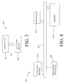
- FIG. 3 is a block diagram of an electronic device in accordance with an embodiment of the invention.
- FIG. 4 is a diagram of an electronic system having devices in accordance with an embodiment of the invention.
- FIG. 5 is a flowchart of a method to reduce impedance between connected integrated circuit devices in accordance with an embodiment of the invention.
- substrate as used in the following description may include any structure having an exposed surface with which to form an IC structure.
- substrate is understood to include semiconductor wafers and is also used to refer to semiconductor structures during processing and may include other layers that have been fabricated thereupon.
- a “wafer” and a “substrate” each include doped and undoped semiconductors, epitaxial semiconductor layers supported by a base semiconductor or insulator, as well as other semiconductor structures well known to one skilled in the art.
- chip is used to refer to IC devices, including logic devices, microprocessors, and various types of memory devices.
- conductor is understood to generally include n-type and p-type semiconductors and doped regions in semiconductors. Conductors may conduct electrical energy including ground potential, various voltage reference levels, and information signals, and may be referred to as wires, lines, cables, buses, planes or traces, depending upon the physical configuration and use of the conductor.
- insulator or “dielectric” is defined to include any material that is less electrically conductive than the materials referred to as conductors or as semiconductors.
- crystalline is understood to not be limited to large single crystals having a specified crystallographic orientation, but may include polycrystalline materials having a large number of moderately sized crystals having various crystallographic orientations.
- amorphous is not limited to a solid material having a completely disordered or glassy structure, but may include materials having some crystalline order over short distances—on the order of ten atomic separations or less.
- horizontal is defined as a plane parallel to the conventional plane or surface of a wafer or substrate, regardless of the orientation of the wafer or substrate.
- vertical refers to a direction perpendicular to the horizontal as defined above. Prepositions, such as “on”, “side” “higher”, “lower”, “over” and “under” are defined with respect to the conventional plane or surface being on the top surface of the wafer or substrate, regardless of the orientation of the wafer or substrate.
- FIG. 1 illustrates a prior art stack 100 of integrated circuit (IC) chips.
- Memory chips such as dynamic random access memory (DRAM), static random access memory (SRAM), content addressable memory (CAM), and flash memory, may be stacked together with similar input output (I/O) pads having a similar function located directly above one another. It may also be convenient to directly connect similar function I/O pads to one another in a series connection of inter-connections, such as wire bonds.
- the stack 100 of ICs may include a number of memory chips 104 , 106 and 108 , which may be located over a logic chip 102 .
- the illustrated example includes three memory chips, but there is no specific limit to the number of memory chips, nor is there any limitation on the types of chips, which may include various types of memory chips, logic chips, microprocessor chips, or other types of chips.
- the logic chip 102 has I/O pads 110 , 112 , 114 , and 116 shown located on one side of the chip. Any of the four sides of a chip may have I/O pads such as those shown in FIG. 1 and the I/O pads may be formed of two or more connected metallic pads to allow for additional external connections, such as the shown wire bonds 140 , 142 , 144 146 , 148 and 150 . Other connection methods may be used including gold bumps, solder bumps, beam leads, and other well known methods. In the example IC stack 100 , only I/O pads 110 and 114 are bonded and in use for interconnection with either the external world or the other chips 104 , 106 and 108 in the stack 100 . I/O pads 112 and 116 are not used in the particular design shown in the figure, and thus the space for the unused I/O pads and the space for the connected power device is wasted in this illustrative design.
- the chip 102 provides power from I/O pad 110 to drive a signal through wirebond 140 to chip 104 , through wirebond 142 to I/O pad 126 on chip 106 , and through wirebond 146 to I/O pad 134 on chip 108 .
- the number and length of the wire bonds that the I/O pad 110 drives to transmit signals to the three shown chips 104 , 106 and 108 may require a larger drive device connected to I/O pad 110 than is usual, and thus may require a specially designed chip rather than an off-the-shelf device with a normal drive device circuit.
- the I/O pad 114 on chip 102 is shown with another prior art stacked IC interconnection method where the I/O pad 114 drives a wire bond 144 to drive a signal to I/O pad 122 on chip 104 .
- the wire bond 148 connecting I/O pad 122 on chip 104 with I/O pad 130 on chip 106 has the same signal provided in series from chip 102 , and that signal is also driven by the I/O pad 114 on chip 102 .
- I/O pad 130 on chip 106 is also connected by wire bond 150 to I/O pad 138 on chip 108 , and the signal is again driven by the same drive device circuit in I/O pad 114 on chip 102 , resulting in a large impedance presented to the signal on its way to reach chip 108 .
- I/O pads 120 and 124 on chip 104 , I/O pads 128 and 132 on chip 106 , and I/O pad 136 on chip 108 do not have any wire bond connections in shown, as is the case for the unused I/O pads 112 and 116 on chip 102 .
- Each of the I/O pads 110 , 112 , 114 and 116 may have an attached output transistor to provide sufficient electrical power to overcome the impedance of the interconnection wiring.
- Impedance is a measure of the delay that charging up an electrical wire causes in the transmission of a signal, and is a combination of the resistance, capacitance and inductance of the interconnect, such as the wire bonds 140 , 142 and 144 shown.
- the output transistor may require a large size and use a large portion of the chip area.
- FIG. 2 illustrates a stack 200 of IC chips connected according to an illustrative embodiment. Multiple interconnected IC devices, such as memory devices and logic devices, are shown in a stacked arrangement.
- the stack 200 includes IC chips 202 , 204 , 206 and 208 .
- Chip 202 may comprise a logic chip or a microprocessor closely connected to memory chips 204 , 206 and 208 , but the present subject matter is not so limited, and may include any number of chips and any combination of chip types.
- embodiments may use a base logic chip, such as chip 202 , as the driver for signals transferred to memory chips 204 , 206 and 208 .
- the drive device connected to an I/O pad on chip 202 should be capable of driving a strong enough signal to rapidly overcome the impedance of inter-chip electrical connections, such as wire bond 240 to I/O pad 218 on chip 204 , as well as the additional wire bonds and connections shown in FIG. 1 .
- the present subject matter includes limiting the number of I/O pads on other chips in direct communications with I/O pad 210 of chip 202 .
- FIG. 2 shows that I/O pad 210 on chip 202 is electrically connected to I/O pad 218 on chip 204 , thus limiting the total electrical impedance by limiting the number of other I/O pads in direct contact.
- High density modules were previously formed by vertically stacking integrated circuit (IC) die (chips) one above another.
- IC integrated circuit
- Each IC in the stack may have a number of input output (I/O) locations (or pads), some of which may not be used in a particular IC design.
- I/O pad on each IC die might be connected (for example by wirebonding) to the I/O pad immediately below and the I/O pad immediately above, resulting in relatively long signal propagation times. This situation may be aggravated by long wire lengths from the drive device on the sending chip, which can be located in a substrate or on a controlling chip at the bottom of the vertical stack of ICs.
- the long wire length and the capacitive loading of the circuitry attached to each I/O pad may thus result in increased impedance and increased signal propagation delay.
- the method of connecting chips in a stack shown in FIG. 2 provides lower impedance (i.e., at least one of low capacitance and low inductance) inter-chip connections by routing inter-chip signals intended to travel to more than a single IC through drive circuits at the unused I/O locations.
- the drive circuit may also be beneficially located in a chip located in the middle of the stack, for example on chip 206 rather than on chip 202 , to reduce the total length of the worst case wire length, and therefore the time required for the signal to travel between the chips.
- I/O pad 210 of chip 202 provides the power for the signal from I/O pad 210 on chip 202 via wirebond 240 to I/O pad 218 on chip 204 .
- Control circuitry associated with I/O pad 218 may then direct the signal to previously unused I/O pad 220 (which is shown as being directly next to the I/O pad 218 but the present subject matter is not so limited and the previously unused I/O pad may be located anywhere on the chip 204 ), which may then use its associated drive device to transmit the signal from I/O pad 220 via wirebond 242 to the previously unused I/O pad 228 on chip 206 .
- Control circuitry associated with I/O pad 228 may then direct the signal to I/O pad 226 , which may use it's associated drive device to transmit the signal via wire bond 246 to I/O pad 234 on chip 208 .
- the same signal may be passed to each and every chip in a stack 200 without using a single I/O pad device driver to provide all of the power needed to transmit the signal to all the other chips.
- the additional control circuitry used to direct the above noted signal may increase the size of a chip from about 0.5% to about 1.0%, depending upon the level of integration of the chips 202 , 204 , 206 and 208 .
- Some embodiments make use of the unused I/O pads, and their associated device drivers and control circuitry to buffer communications to the outside world, including other chips located in a stacked arrangement and closely coupled to a primary chip, and the printed circuit board (PCB) upon which the primary chip may be connected.
- the signal delay can thus be reduced by using previously unused I/O pads, the associated control circuitry and device drivers to reduce the number of other I/O pads and external circuits to which each I/O pad is directly connected.
- FIG. 2 shows no more than one electrical connection (such as wire bonds 240 , 242 , 244 , 246 , 248 and 250 ) from each I/O pad (such as 210 , 214 , 218 , 220 , 222 , 224 , 226 , 228 , 230 232 , 234 and 238 ) as compared to the multiple wire bonds shown in FIG. 1 , the present subject matter is not so limited.
- the FIG. 2 arrangement may be considered as a best case situation when there are sufficient numbers of previously unused I/O pads to have a one-to-one correspondence between unused I/O pad drivers and I/O pads that can benefit from being coupled to them.
- a goal is to use the unused I/O pads and drivers to obtain the shown situation of a single connection from each I/O pad.
- the impedance environment would appear to be approximately the same as in a monolithic device, and the resulting signal delays will be minimized as compared to a stack of ICs being driven by a single device driver and I/O pad.
- the present subject matter may include an approximately 1% increase in chip area related to adding control circuitry to control the routing of the signals to the previously unused I/O pads.
- FIG. 3 is a block diagram of an electronic device 306 in accordance with an embodiment of the invention.
- Electronic system 300 includes a controller 302 , a bus 304 , and an electronic device 306 , where bus 304 provides electrical conductivity between controller 302 and electronic device 306 .
- controller 302 and/or electronic device 306 include an embodiment for a portion of the device 306 having logic and memory chips stacked and interconnected as previously discussed herein.
- the device 306 may include one or more chip stacks that are similar to or identical to the stack 200 shown in FIG. 2 .
- Electronic system 300 may include, but is not limited to, information handling devices, wireless systems, telecommunication systems, fiber optic systems, electro-optic systems, and computers.
- FIG. 4 is a diagram of an electronic system 400 having devices in accordance with an embodiment of the invention.
- the system 400 includes a controller 402 and a memory 406 .
- Controller 402 and/or memory 406 may each include a potion of the circuit having IC devices and memory chips stacked and connected in accordance with the disclosed embodiments.
- the controller 402 and memory 406 may include one or more chip stacks that are similar to or identical to the stack 200 shown in FIG. 2 .
- System 400 also includes an electronic apparatus 408 , and a bus 404 , where bus 404 may provide electrical conductivity and data transmission between controller 402 and electronic apparatus 408 , and between controller 402 and memory 406 .
- Bus 404 may include an address bus, a data bus, and a control bus, each independently configured. Bus 404 also uses common conductive lines for providing address, data, and/or control, the use of which may be regulated by controller 402 .
- electronic apparatus 408 includes additional memory devices configured similarly to or identically to memory 406 .
- An embodiment includes an additional peripheral device or devices 410 coupled to bus 404 .
- controller 402 is a processor.
- bus 404 , electronic apparatus 408 , and peripheral device or devices 410 may include ICs being stacked in accordance with the disclosed embodiments.
- the bus 404 , the electronic apparatus 408 , and the peripheral device 410 may include one or more chip stacks that are similar to or identical to the stack 200 shown in FIG. 2 .
- System 400 may include, but is not limited to, information handling devices, telecommunication systems, and computers.
- Peripheral devices 410 may include displays, additional memory, or other control devices operating with controller 402 and/or memory 406 .
- FIG. 5 is a flowchart of a method to reduce impedance between connected integrated circuit devices in accordance with an embodiment of the invention.
- the reduction of impedance presented to signals propagating within a chip stack may be obtained in various combinations of the described embodiments, including a method of electrically connecting a plurality of integrated circuit devices 502 , by first determining which electrical connections (preferably the input/output or I/O pads) on each integrated circuit device are not used in the circuit design 504 , and which electrical connections or I/O pads are used. Then determining which electrical paths connecting the ICs or chips in the stack have the largest electrical impedance value 506 and interconnecting the chips by routing portions of the highest impedance path 508 through some of the unused electrical connections 510 to spread the electrical load.
- electrical connections preferably the input/output or I/O pads
- the routing for the largest electrical impedance value path may be arranged to have a single electric connection between each I/O pad along the signal path.
- the extra control circuitry may add about 0.5 to 1.0% to the circuitry area used on the chip.
- the I/O pads of one IC connected (at least electrically) to another IC by connecting each I/O pad to only one other IC in the vertical stack.
- the I/O pads may include a connection to an unused connection of another one of the ICs in the vertical stack, and the electrical connection may include wire bonds which may be on at least one edge of the ICs.
- a stack of ICs may have the IC with the largest area the lowest in the vertical stack, with a second largest area one of the plurality of ICs the next higher IC in the vertical stack, and a third largest area IC being the third IC in the vertical stack, and located above the second largest area IC.
- the ICs are not all in descending size order it may be beneficial to form vertical bumps attached either between two facing top surfaces of the ICs in the vertical stack, or connecting a top surface of a lower IC to input/output pads on a bottom surface of an upper IC.
- the top to bottom attachment may benefit from (and include) the use of through silicon vias that go from the top surface to the bottom surface of the IC.
- Another method of electrically connecting a plurality of IC devices includes determining a plurality of unused electrical connections on each IC. Then determining a first set of electrical paths between the ICs that have higher electrical impedance value than other electrical paths, and could benefit from reduced impedance. Adding additional interconnections for the first set of paths by adding some of the unused electrical connections into the first set of paths to reduce the impedance.
- a circuit having the described arrangement of low impedance interconnections includes ICs attached in a vertical stack where each individual IC includes both electrical connections used in a selected circuit design and electrical connections not used in the circuit design.
- the electrical path connecting the ICs includes at least one of the otherwise unused electrical connections on at least one IC to spread the electrical load and utilize otherwise unused I/O pads and their associated drive circuitry.
- the interconnection may be more easily constructed if each one of the ICs in the vertical stack has a different physical dimension and can be stacked in decreasing size order with the largest physical dimension located at the bottom and the smallest physical dimension located at the top of the vertical stack.
- Each of the ICs in the vertical stack includes a plurality of signal output pads on the edge for electrical connections, and the signal output pads may be on all four sides of the IC.
- the interconnection are arranged to reduce impedance by setting each of the signal output pads to be connected to only one of the other ICs in the vertical stack.
- Control circuitry on the signal output pads of a first IC may be used to route an incoming signal to an unused signal output pad for transmission to a second IC, and so utilize the unused portions of the first IC.
- the signal output pads may be connected to selected other signal output pads on other ICs by wire bonds, flexible tape, solder bumps, or gold bumps, depending upon the relative sizes of the various ICs and the technology, and it may be beneficial to limit each electrical connection to a single connection to another IC.
- a system having the described arrangement of low impedance interconnections may include a controller connected to an electronic device having a plurality of ICs coupled to the controller. Each of the ICs may have electrical connections to the other integrated circuits. Each IC may have I/O pads and drive circuits used in a selected circuit design, and I/O pads and drive circuits not used in the selected circuit design. Additional inter IC connections using the I/O pads that are unused and added to the electrical path may reduce the overall impedance. In this fashion the electrical path connects each one of the plurality of integrated circuits to each other one of the plurality of integrated circuits with a single electrical path similar to the situation found in monolithic device.
Abstract
Description
Claims (23)
Priority Applications (4)
| Application Number | Priority Date | Filing Date | Title |
|---|---|---|---|
| US12/197,869 US8001513B2 (en) | 2008-08-25 | 2008-08-25 | Integrated circuit apparatus, systems, and methods |
| US13/208,986 US8245176B2 (en) | 2008-08-25 | 2011-08-12 | Integrated circuit apparatus, systems, and methods |
| US13/569,500 US8499271B2 (en) | 2008-08-25 | 2012-08-08 | Integrated circuit apparatus, systems, and methods |
| US13/953,427 US8832631B2 (en) | 2008-08-25 | 2013-07-29 | Integrated circuit apparatus, systems, and methods |
Applications Claiming Priority (1)
| Application Number | Priority Date | Filing Date | Title |
|---|---|---|---|
| US12/197,869 US8001513B2 (en) | 2008-08-25 | 2008-08-25 | Integrated circuit apparatus, systems, and methods |
Related Child Applications (1)
| Application Number | Title | Priority Date | Filing Date |
|---|---|---|---|
| US13/208,986 Continuation US8245176B2 (en) | 2008-08-25 | 2011-08-12 | Integrated circuit apparatus, systems, and methods |
Publications (2)
| Publication Number | Publication Date |
|---|---|
| US20100047966A1 US20100047966A1 (en) | 2010-02-25 |
| US8001513B2 true US8001513B2 (en) | 2011-08-16 |
Family
ID=41696754
Family Applications (4)
| Application Number | Title | Priority Date | Filing Date |
|---|---|---|---|
| US12/197,869 Active 2029-08-25 US8001513B2 (en) | 2008-08-25 | 2008-08-25 | Integrated circuit apparatus, systems, and methods |
| US13/208,986 Active US8245176B2 (en) | 2008-08-25 | 2011-08-12 | Integrated circuit apparatus, systems, and methods |
| US13/569,500 Active US8499271B2 (en) | 2008-08-25 | 2012-08-08 | Integrated circuit apparatus, systems, and methods |
| US13/953,427 Active US8832631B2 (en) | 2008-08-25 | 2013-07-29 | Integrated circuit apparatus, systems, and methods |
Family Applications After (3)
| Application Number | Title | Priority Date | Filing Date |
|---|---|---|---|
| US13/208,986 Active US8245176B2 (en) | 2008-08-25 | 2011-08-12 | Integrated circuit apparatus, systems, and methods |
| US13/569,500 Active US8499271B2 (en) | 2008-08-25 | 2012-08-08 | Integrated circuit apparatus, systems, and methods |
| US13/953,427 Active US8832631B2 (en) | 2008-08-25 | 2013-07-29 | Integrated circuit apparatus, systems, and methods |
Country Status (1)
| Country | Link |
|---|---|
| US (4) | US8001513B2 (en) |
Cited By (3)
| Publication number | Priority date | Publication date | Assignee | Title |
|---|---|---|---|---|
| US20120032706A1 (en) * | 2010-08-04 | 2012-02-09 | Kyoung Nam Kim | Multi-chip package |
| US8245176B2 (en) | 2008-08-25 | 2012-08-14 | Micron Technology, Inc. | Integrated circuit apparatus, systems, and methods |
| US20120211867A1 (en) * | 2011-02-17 | 2012-08-23 | Apple Inc. | Side-mounted controller and methods for making the same |
Families Citing this family (6)
| Publication number | Priority date | Publication date | Assignee | Title |
|---|---|---|---|---|
| JP2010161102A (en) * | 2009-01-06 | 2010-07-22 | Elpida Memory Inc | Semiconductor device |
| KR101086875B1 (en) * | 2009-09-30 | 2011-11-25 | 주식회사 하이닉스반도체 | Data transmission circuit and semiconductor apparatus including the same |
| US8966419B2 (en) * | 2012-07-11 | 2015-02-24 | Taiwan Semiconductor Manufacturing Co., Ltd. | System and method for testing stacked dies |
| US8561001B1 (en) * | 2012-07-11 | 2013-10-15 | Taiwan Semiconductor Manufacturing Co., Ltd. | System and method for testing stacked dies |
| KR102041500B1 (en) | 2013-03-08 | 2019-11-06 | 삼성전자 주식회사 | Semiconductor package |
| KR102215826B1 (en) * | 2014-12-22 | 2021-02-16 | 삼성전자주식회사 | Stacked memory chip having reduced input-output load, memory module and memory system including the same |
Citations (9)
| Publication number | Priority date | Publication date | Assignee | Title |
|---|---|---|---|---|
| US4970454A (en) * | 1986-12-09 | 1990-11-13 | Texas Instruments Incorporated | Packaged semiconductor device with test circuits for determining fabrication parameters |
| US5454160A (en) * | 1993-12-03 | 1995-10-03 | Ncr Corporation | Apparatus and method for stacking integrated circuit devices |
| US5910010A (en) * | 1994-04-26 | 1999-06-08 | Hitachi, Ltd. | Semiconductor integrated circuit device, and process and apparatus for manufacturing the same |
| US6066561A (en) * | 1997-12-19 | 2000-05-23 | Lsi Logic Corporation | Apparatus and method for electrical determination of delamination at one or more interfaces within a semiconductor wafer |
| US6128201A (en) * | 1997-05-23 | 2000-10-03 | Alpine Microsystems, Inc. | Three dimensional mounting assembly for integrated circuits |
| US6173435B1 (en) * | 1998-02-20 | 2001-01-09 | Lsi Logic Corporation | Internal clock handling in synthesis script |
| US6205572B1 (en) * | 1998-02-20 | 2001-03-20 | Lsi Logic Corporation | Buffering tree analysis in mapped design |
| US6686656B1 (en) * | 2003-01-13 | 2004-02-03 | Kingston Technology Corporation | Integrated multi-chip chip scale package |
| US6686768B2 (en) * | 2001-07-05 | 2004-02-03 | Alan Elbert Comer | Electrically-programmable interconnect architecture for easily-configurable stacked circuit arrangements |
Family Cites Families (4)
| Publication number | Priority date | Publication date | Assignee | Title |
|---|---|---|---|---|
| US7259464B1 (en) * | 2000-05-09 | 2007-08-21 | Micron Technology, Inc. | Vertical twist scheme for high-density DRAMs |
| US7833895B2 (en) | 2008-05-12 | 2010-11-16 | Texas Instruments Incorporated | TSVS having chemically exposed TSV tips for integrated circuit devices |
| US8006216B1 (en) * | 2008-06-06 | 2011-08-23 | Magma Design Automation, Inc. | Dynamic push for topological routing of semiconductor packages |
| US8001513B2 (en) | 2008-08-25 | 2011-08-16 | Micron Technology, Inc. | Integrated circuit apparatus, systems, and methods |
-
2008
- 2008-08-25 US US12/197,869 patent/US8001513B2/en active Active
-
2011
- 2011-08-12 US US13/208,986 patent/US8245176B2/en active Active
-
2012
- 2012-08-08 US US13/569,500 patent/US8499271B2/en active Active
-
2013
- 2013-07-29 US US13/953,427 patent/US8832631B2/en active Active
Patent Citations (9)
| Publication number | Priority date | Publication date | Assignee | Title |
|---|---|---|---|---|
| US4970454A (en) * | 1986-12-09 | 1990-11-13 | Texas Instruments Incorporated | Packaged semiconductor device with test circuits for determining fabrication parameters |
| US5454160A (en) * | 1993-12-03 | 1995-10-03 | Ncr Corporation | Apparatus and method for stacking integrated circuit devices |
| US5910010A (en) * | 1994-04-26 | 1999-06-08 | Hitachi, Ltd. | Semiconductor integrated circuit device, and process and apparatus for manufacturing the same |
| US6128201A (en) * | 1997-05-23 | 2000-10-03 | Alpine Microsystems, Inc. | Three dimensional mounting assembly for integrated circuits |
| US6066561A (en) * | 1997-12-19 | 2000-05-23 | Lsi Logic Corporation | Apparatus and method for electrical determination of delamination at one or more interfaces within a semiconductor wafer |
| US6173435B1 (en) * | 1998-02-20 | 2001-01-09 | Lsi Logic Corporation | Internal clock handling in synthesis script |
| US6205572B1 (en) * | 1998-02-20 | 2001-03-20 | Lsi Logic Corporation | Buffering tree analysis in mapped design |
| US6686768B2 (en) * | 2001-07-05 | 2004-02-03 | Alan Elbert Comer | Electrically-programmable interconnect architecture for easily-configurable stacked circuit arrangements |
| US6686656B1 (en) * | 2003-01-13 | 2004-02-03 | Kingston Technology Corporation | Integrated multi-chip chip scale package |
Cited By (7)
| Publication number | Priority date | Publication date | Assignee | Title |
|---|---|---|---|---|
| US8245176B2 (en) | 2008-08-25 | 2012-08-14 | Micron Technology, Inc. | Integrated circuit apparatus, systems, and methods |
| US8499271B2 (en) | 2008-08-25 | 2013-07-30 | Micron Technology, Inc. | Integrated circuit apparatus, systems, and methods |
| US8832631B2 (en) | 2008-08-25 | 2014-09-09 | Micron Technology, Inc. | Integrated circuit apparatus, systems, and methods |
| US20120032706A1 (en) * | 2010-08-04 | 2012-02-09 | Kyoung Nam Kim | Multi-chip package |
| US8344754B2 (en) * | 2010-08-04 | 2013-01-01 | Hynix Semiconductor Inc. | Multi-chip package |
| US20120211867A1 (en) * | 2011-02-17 | 2012-08-23 | Apple Inc. | Side-mounted controller and methods for making the same |
| US8587088B2 (en) * | 2011-02-17 | 2013-11-19 | Apple Inc. | Side-mounted controller and methods for making the same |
Also Published As
| Publication number | Publication date |
|---|---|
| US20110298122A1 (en) | 2011-12-08 |
| US8832631B2 (en) | 2014-09-09 |
| US8245176B2 (en) | 2012-08-14 |
| US8499271B2 (en) | 2013-07-30 |
| US20120299198A1 (en) | 2012-11-29 |
| US20100047966A1 (en) | 2010-02-25 |
| US20130307164A1 (en) | 2013-11-21 |
Similar Documents
| Publication | Publication Date | Title |
|---|---|---|
| US8832631B2 (en) | Integrated circuit apparatus, systems, and methods | |
| US11693801B2 (en) | Stacked semiconductor device assembly in computer system | |
| CN108155174B (en) | Semiconductor memory device including stacked chips and memory module having the same | |
| EP0683968B1 (en) | Module comprising ic memory stack dedicated to and structurally combined with an ic microprocessor | |
| KR100800486B1 (en) | Semiconductor memory device having an improved signal transmission path and driving method thereof | |
| US20100052111A1 (en) | Stacked-chip device | |
| US8021928B1 (en) | System and method for routing supply voltages or other signals between side-by-side die and a lead frame for system in a package (SIP) devices | |
| US9070570B2 (en) | Stack packages having token ring loops | |
| US20230163099A1 (en) | Semiconductor package | |
| TWI819060B (en) | Semiconductor packages | |
| US7714450B2 (en) | On-die bond wires system and method for enhancing routability of a redistribution layer | |
| US8288852B2 (en) | Semiconductor device | |
| CN116367540B (en) | Semiconductor structure and forming method thereof | |
| KR20230029123A (en) | Semiconductor packages | |
| JP2002076176A (en) | Ball grid array package |
Legal Events
| Date | Code | Title | Description |
|---|---|---|---|
| AS | Assignment |
Owner name: MICRON TECHNOLOGY, INC.,IDAHO Free format text: ASSIGNMENT OF ASSIGNORS INTEREST;ASSIGNOR:SILVESTRI, PAUL A.;REEL/FRAME:021536/0180 Effective date: 20080820 Owner name: MICRON TECHNOLOGY, INC., IDAHO Free format text: ASSIGNMENT OF ASSIGNORS INTEREST;ASSIGNOR:SILVESTRI, PAUL A.;REEL/FRAME:021536/0180 Effective date: 20080820 |
|
| FEPP | Fee payment procedure |
Free format text: PAYOR NUMBER ASSIGNED (ORIGINAL EVENT CODE: ASPN); ENTITY STATUS OF PATENT OWNER: LARGE ENTITY |
|
| STCF | Information on status: patent grant |
Free format text: PATENTED CASE |
|
| FPAY | Fee payment |
Year of fee payment: 4 |
|
| AS | Assignment |
Owner name: U.S. BANK NATIONAL ASSOCIATION, AS COLLATERAL AGENT, CALIFORNIA Free format text: SECURITY INTEREST;ASSIGNOR:MICRON TECHNOLOGY, INC.;REEL/FRAME:038669/0001 Effective date: 20160426 Owner name: U.S. BANK NATIONAL ASSOCIATION, AS COLLATERAL AGEN Free format text: SECURITY INTEREST;ASSIGNOR:MICRON TECHNOLOGY, INC.;REEL/FRAME:038669/0001 Effective date: 20160426 |
|
| AS | Assignment |
Owner name: MORGAN STANLEY SENIOR FUNDING, INC., AS COLLATERAL AGENT, MARYLAND Free format text: PATENT SECURITY AGREEMENT;ASSIGNOR:MICRON TECHNOLOGY, INC.;REEL/FRAME:038954/0001 Effective date: 20160426 Owner name: MORGAN STANLEY SENIOR FUNDING, INC., AS COLLATERAL Free format text: PATENT SECURITY AGREEMENT;ASSIGNOR:MICRON TECHNOLOGY, INC.;REEL/FRAME:038954/0001 Effective date: 20160426 |
|
| AS | Assignment |
Owner name: U.S. BANK NATIONAL ASSOCIATION, AS COLLATERAL AGENT, CALIFORNIA Free format text: CORRECTIVE ASSIGNMENT TO CORRECT THE REPLACE ERRONEOUSLY FILED PATENT #7358718 WITH THE CORRECT PATENT #7358178 PREVIOUSLY RECORDED ON REEL 038669 FRAME 0001. ASSIGNOR(S) HEREBY CONFIRMS THE SECURITY INTEREST;ASSIGNOR:MICRON TECHNOLOGY, INC.;REEL/FRAME:043079/0001 Effective date: 20160426 Owner name: U.S. BANK NATIONAL ASSOCIATION, AS COLLATERAL AGEN Free format text: CORRECTIVE ASSIGNMENT TO CORRECT THE REPLACE ERRONEOUSLY FILED PATENT #7358718 WITH THE CORRECT PATENT #7358178 PREVIOUSLY RECORDED ON REEL 038669 FRAME 0001. ASSIGNOR(S) HEREBY CONFIRMS THE SECURITY INTEREST;ASSIGNOR:MICRON TECHNOLOGY, INC.;REEL/FRAME:043079/0001 Effective date: 20160426 |
|
| AS | Assignment |
Owner name: JPMORGAN CHASE BANK, N.A., AS COLLATERAL AGENT, ILLINOIS Free format text: SECURITY INTEREST;ASSIGNORS:MICRON TECHNOLOGY, INC.;MICRON SEMICONDUCTOR PRODUCTS, INC.;REEL/FRAME:047540/0001 Effective date: 20180703 Owner name: JPMORGAN CHASE BANK, N.A., AS COLLATERAL AGENT, IL Free format text: SECURITY INTEREST;ASSIGNORS:MICRON TECHNOLOGY, INC.;MICRON SEMICONDUCTOR PRODUCTS, INC.;REEL/FRAME:047540/0001 Effective date: 20180703 |
|
| AS | Assignment |
Owner name: MICRON TECHNOLOGY, INC., IDAHO Free format text: RELEASE BY SECURED PARTY;ASSIGNOR:U.S. BANK NATIONAL ASSOCIATION, AS COLLATERAL AGENT;REEL/FRAME:047243/0001 Effective date: 20180629 |
|
| MAFP | Maintenance fee payment |
Free format text: PAYMENT OF MAINTENANCE FEE, 8TH YEAR, LARGE ENTITY (ORIGINAL EVENT CODE: M1552); ENTITY STATUS OF PATENT OWNER: LARGE ENTITY Year of fee payment: 8 |
|
| AS | Assignment |
Owner name: MICRON TECHNOLOGY, INC., IDAHO Free format text: RELEASE BY SECURED PARTY;ASSIGNOR:MORGAN STANLEY SENIOR FUNDING, INC., AS COLLATERAL AGENT;REEL/FRAME:050937/0001 Effective date: 20190731 |
|
| AS | Assignment |
Owner name: MICRON TECHNOLOGY, INC., IDAHO Free format text: RELEASE BY SECURED PARTY;ASSIGNOR:JPMORGAN CHASE BANK, N.A., AS COLLATERAL AGENT;REEL/FRAME:051028/0001 Effective date: 20190731 Owner name: MICRON SEMICONDUCTOR PRODUCTS, INC., IDAHO Free format text: RELEASE BY SECURED PARTY;ASSIGNOR:JPMORGAN CHASE BANK, N.A., AS COLLATERAL AGENT;REEL/FRAME:051028/0001 Effective date: 20190731 |
|
| MAFP | Maintenance fee payment |
Free format text: PAYMENT OF MAINTENANCE FEE, 12TH YEAR, LARGE ENTITY (ORIGINAL EVENT CODE: M1553); ENTITY STATUS OF PATENT OWNER: LARGE ENTITY Year of fee payment: 12 |