US7990779B2 - Method of operating semiconductor devices - Google Patents
Method of operating semiconductor devices Download PDFInfo
- Publication number
- US7990779B2 US7990779B2 US12/585,540 US58554009A US7990779B2 US 7990779 B2 US7990779 B2 US 7990779B2 US 58554009 A US58554009 A US 58554009A US 7990779 B2 US7990779 B2 US 7990779B2
- Authority
- US
- United States
- Prior art keywords
- voltage
- gate
- drain
- region
- gate voltage
- Prior art date
- Legal status (The legal status is an assumption and is not a legal conclusion. Google has not performed a legal analysis and makes no representation as to the accuracy of the status listed.)
- Active, expires
Links
Images


Classifications
-
- G—PHYSICS
- G11—INFORMATION STORAGE
- G11C—STATIC STORES
- G11C11/00—Digital stores characterised by the use of particular electric or magnetic storage elements; Storage elements therefor
- G11C11/21—Digital stores characterised by the use of particular electric or magnetic storage elements; Storage elements therefor using electric elements
- G11C11/34—Digital stores characterised by the use of particular electric or magnetic storage elements; Storage elements therefor using electric elements using semiconductor devices
- G11C11/40—Digital stores characterised by the use of particular electric or magnetic storage elements; Storage elements therefor using electric elements using semiconductor devices using transistors
- G11C11/401—Digital stores characterised by the use of particular electric or magnetic storage elements; Storage elements therefor using electric elements using semiconductor devices using transistors forming cells needing refreshing or charge regeneration, i.e. dynamic cells
- G11C11/403—Digital stores characterised by the use of particular electric or magnetic storage elements; Storage elements therefor using electric elements using semiconductor devices using transistors forming cells needing refreshing or charge regeneration, i.e. dynamic cells with charge regeneration common to a multiplicity of memory cells, i.e. external refresh
- G11C11/404—Digital stores characterised by the use of particular electric or magnetic storage elements; Storage elements therefor using electric elements using semiconductor devices using transistors forming cells needing refreshing or charge regeneration, i.e. dynamic cells with charge regeneration common to a multiplicity of memory cells, i.e. external refresh with one charge-transfer gate, e.g. MOS transistor, per cell
-
- H—ELECTRICITY
- H10—SEMICONDUCTOR DEVICES; ELECTRIC SOLID-STATE DEVICES NOT OTHERWISE PROVIDED FOR
- H10D—INORGANIC ELECTRIC SEMICONDUCTOR DEVICES
- H10D30/00—Field-effect transistors [FET]
- H10D30/60—Insulated-gate field-effect transistors [IGFET]
- H10D30/711—Insulated-gate field-effect transistors [IGFET] having floating bodies
-
- G—PHYSICS
- G11—INFORMATION STORAGE
- G11C—STATIC STORES
- G11C2211/00—Indexing scheme relating to digital stores characterized by the use of particular electric or magnetic storage elements; Storage elements therefor
- G11C2211/401—Indexing scheme relating to cells needing refreshing or charge regeneration, i.e. dynamic cells
- G11C2211/4016—Memory devices with silicon-on-insulator cells
Definitions
- Example embodiments relate to methods of operating semiconductor devices, and more particularly, to methods of operating semiconductor devices that include adjusting gate voltage level in a hold mode.
- a conventional memory for example, a DRAM, may include one transistor and one capacitor as a memory cell.
- a memory including one transistor (1T) and no capacitor as a memory cell referred to as ‘a capacitor-less memory or 1-T DRAM’, has been studied.
- the 1-T DRAM may be simple to manufacture and it may be easy to make a memory device with larger density.
- Example embodiments provide a method of operating a semiconductor device that includes adjusting a gate voltage level in a hold mode.
- a method of operating a semiconductor device having at least one memory cell including a drain region, a source region, a floating body region, and a gate electrode including: applying a first gate voltage to the gate electrode and a first drain voltage to the drain region, in a write mode, to change a data state of the memory cell to a first state; applying an adjustable second gate voltage to the gate electrode and a second drain voltage to the drain region, in a hold mode after the write mode.
- the voltage level of the second gate voltage may be adjusted so that an amount of carriers (e.g., holes) stored in the floating body region may be adjusted.
- the voltage level of the second gate voltage may be adjustable in a range where the voltage level of the second gate voltage is negative.
- the voltage level of the second gate voltage may be less than the voltage level of the first gate voltage, and the voltage level of the second drain voltage may be less than the voltage level of the first drain voltage.
- a method of operating at least one semiconductor device including a drain region, a source region, a floating body region, and a gate pattern
- the method including: applying a first gate voltage to the gate pattern and a first drain voltage to the drain region, in a write mode, to change a data state of the semiconductor device to a first state; and applying a second gate voltage to the gate pattern and a second drain voltage to the drain region, in a hold mode after the write mode, the difference between the first gate voltage and the second gate voltage being an adjustable difference.
- a method of operating at least one semiconductor device including a drain region, a source region, a floating body region, and a gate electrode
- the method including: applying an activation period of a gate voltage pulse to the gate electrode and applying an activation period of a drain voltage pulse to the drain region, in a write mode, to change the data state of the semiconductor device to a first state; applying a deactivation period of the gate voltage pulse to the gate electrode, a voltage level of the deactivation period of the voltage pulse being adjustable, and applying a deactivation period of the drain voltage pulse to the drain region, in a hold mode after the write mode.
- FIGS. 1-14 represent non-limiting, example embodiments as described herein.
- FIG. 1 is a cross-sectional diagram illustrating an example memory cell of a one transistor-dynamic random access memory (1T-DRAM) device according to example embodiments;
- FIG. 2 is a circuit diagram of the memory cell of FIG. 1 ;
- FIG. 3 is a cross-sectional diagram illustrating carrier generation in a write mode of the memory cell of FIG. 1 ;
- FIG. 4 is a cross-sectional diagram illustrating carrier storage after the write mode of the memory cell of FIG. 3 ;
- FIG. 5 is a cross-sectional diagram illustrating the absence of carrier storage in the memory cell of FIG. 1 ;
- FIG. 6 is a graph of drain/source current (I ds ) as a function of gate voltage (V g ) for a read operation, illustrating a sense margin of the memory cell of FIG. 1 ;
- FIG. 7 is a graph of voltage as a function of time, illustrating voltage pulses divided into a write mode and a hold mode, according to example embodiments
- FIG. 8 is a cross-sectional diagram illustrating a carrier concentration distribution generated in the write mode of FIG. 7 ;
- FIGS. 9-11 are cross-sectional diagrams illustrating carrier concentration distributions generated in the hold mode of FIG. 7 ;
- FIG. 12 is a graph of drain/source current (I ds ) as a function of gate voltage (V) of a read operation, illustrating sense margins resulting from gate voltage pulses applied in a write mode and a hold mode, according to example embodiments;
- FIGS. 13 and 14 are cross-sectional diagrams illustrating memory cells of 1T-DRAM devices according to example embodiments.
- Example embodiments will now be described more fully with reference to the accompanying drawings, in which example embodiments are shown.
- Example embodiments may, however, be embodied in many different forms and should not be construed as being limited to the embodiments set forth herein; rather, these embodiments are provided so that this disclosure will be thorough and complete, and will fully convey the concept of example embodiments to those of ordinary skill in the art.
- the thicknesses of layers and regions are exaggerated for clarity.
- Like reference numerals in the drawings denote like elements, and thus their description will be omitted.
- first”, “second”, etc. may be used herein to describe various elements, components, regions, layers and/or sections, these elements, components, regions, layers and/or sections should not be limited by these terms. These terms are only used to distinguish one element, component, region, layer or section from another element, component, region, layer or section. Thus, a first element, component, region, layer or section discussed below could be termed a second element, component, region, layer or section without departing from the teachings of example embodiments.
- spatially relative terms such as “beneath,” “below,” “lower,” “above,” “upper” and the like, may be used herein for ease of description to describe one element or feature's relationship to another element(s) or feature(s) as illustrated in the figures. It will be understood that the spatially relative terms are intended to encompass different orientations of the device in use or operation in addition to the orientation depicted in the figures. For example, if the device in the figures is turned over, elements described as “below” or “beneath” other elements or features would then be oriented “above” the other elements or features. Thus, the exemplary term “below” can encompass both an orientation of above and below. The device may be otherwise oriented (rotated 90 degrees or at other orientations) and the spatially relative descriptors used herein interpreted accordingly.
- Example embodiments are described herein with reference to cross-sectional illustrations that are schematic illustrations of idealized embodiments (and intermediate structures) of example embodiments. As such, variations from the shapes of the illustrations as a result, for example, of manufacturing techniques and/or tolerances, are to be expected. Thus, example embodiments should not be construed as limited to the particular shapes of regions illustrated herein but are to include deviations in shapes that result, for example, from manufacturing. For example, an implanted region illustrated as a rectangle may have rounded or curved features and/or a gradient of implant concentration at its edges rather than a binary change from implanted to non-implanted region.
- a buried region formed by implantation may result in some implantation in the region between the buried region and the surface through which the implantation takes place.
- the regions illustrated in the figures are schematic in nature and their shapes are not intended to illustrate the actual shape of a region of a device and are not intended to limit the scope of example embodiments.
- FIG. 1 is a cross-sectional diagram illustrating an example memory cell 100 of a 1T-DRAM device, which may be operated using methods of operating semiconductor devices according to example embodiments.
- a memory cell 100 of the 1T-DRAM device of FIG. 1 may include an insulating layer 110 on a semiconductor substrate 120 , a body region 170 , a gate electrode 130 , a source electrode 162 , a drain electrode 164 , a source region 140 , and a drain region 150 .
- the source region 140 and the drain region 150 may be doped.
- the source region 140 and the drain region 150 may be interchanged with each other, and therefore the source electrode 162 and the drain electrode 164 may be interchanged with each other.
- a gate voltage, a drain voltage, and a source voltage, which are applied to the gate electrode 130 , the source electrode 162 , and the drain electrode 164 , respectively, may be adjusted so that data can be written, erased, and/or read in the memory cell 100 of the 1T-DRAM device.
- FIG. 2 is a circuit diagram of the example memory cell 100 of FIG. 1 connected to a source line SL, a bit line BL and a word line WL.
- the source region 140 may be connected to the source line SL through the source electrode 162 and the drain region 150 may be connected to the bit line BL through the drain electrode 164 .
- the source voltage may be supplied to the source region 140 through the source line SL and the drain voltage may be supplied to the drain region 150 through the bit line BL.
- the bit line BL and the source line SL are particularly shown in FIG. 2 , in a reverse operation of the 1T-DRAM device, the source line SL may become the bit line BL and the bit line BL may become the source line SL.
- the gate electrode 130 may be connected to a word line WL and the gate voltage may be supplied to the gate electrode 130 through the word line WL.
- FIG. 3 is a cross-sectional diagram illustrating carrier generation in a write mode of the memory cell 100 of FIG. 1 .
- FIG. 4 is a cross-sectional diagram illustrating carrier storage after the write mode of the memory cell of FIG. 3 .
- FIG. 5 is a cross-sectional diagram illustrating the absence of carrier storage in the memory cell of FIG. 1 .
- a plurality of electron-hole pairs may be generated under a given voltage bias condition by impact ionization or avalanche breakdown in a portion of the memory cell where the body region 170 and the drain region 150 contact each other, illustrated in FIG. 3 .
- the generated electrons may be moved into the drain region 150 and the generated holes (majority carriers) may be moved into the body region 170 under the given voltage bias condition.
- majority carriers generated due to impact ionization may be stored in the body region 170 .
- Carrier concentration in a region indicated by intermediate shading is higher than a carrier concentration in a region indicated by light shading.
- the memory cell 100 When carriers are stored in the body region 170 (e.g., high and/or increased carrier concentration) the memory cell 100 may have a data value of “1”. Referring to FIG. 5 , when carriers are not generated in the write mode, or are removed in an erase mode, carriers are not stored in the body region 170 . A region indicated by light shading indicates that carrier concentration is low relative to a region in which carriers are stored. When carriers are not stored in the body region 170 (e.g., low and/or decreased carrier concentration) the memory cell 100 may have a data value of “0”.
- data may be read from the memory cell 100 of 1T-DRAM device by measuring the amount of current that flows between the drain region 150 and the source region 140 when a gate read voltage is applied to the gate electrode 130 .
- the amount of current that flows between the drain region 150 and the source region 140 may be high and/or increased.
- the amount of current that flows between the drain region 150 and the source region 140 may be small and/or decreased.
- FIG. 6 is a graph of drain/source current (I ds ) as a function of gate voltage (V g ), illustrating a sense margin of the memory cell of FIG. 1 .
- I ds drain/source current
- V g gate voltage
- the data value of the memory cell 100 of the 1T-DRAM device is “1” and a read voltage between a first gate voltage V g1 and a second gate voltage V g2 is applied to the gate electrode 130 , a large and/or increased current I 1 may flow between the source region 140 and the drain region 150 . If the data value of the 1T-DRAM device 100 is “0” and the read voltage between a first gate voltage V g1 and a second gate voltage V g2 is applied to the gate electrode 130 , a small and/or decreased current I 2 may flow between the source region 140 and the drain region 150 .
- the data value stored in the memory cell of a 1T-DRAM device may be determined by sensing whether the sense current is I 1 (e.g., data value “1”) or I 2 (e.g., data value “0”).
- a difference between the first gate voltage V g , and the second gate voltage V g2 is referred to as a sense margin, denoted by ⁇ Vth in FIG. 6 .
- the sense margin refers to the difference between the threshold voltage of the memory cell of a 1T-DRAM device when carriers are stored and when carriers are not stored.
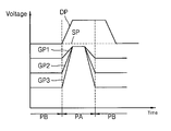
- FIG. 7 is a graph of voltage as a function of time, illustrating voltage pulses divided into a write mode PA and a hold mode PB, according to example embodiments.
- the semiconductor device including the memory cell of a 1T-DRAM may operate in a write mode PA and a hold mode PB.
- Carriers may be generated in the write mode PA and then stored in the hold mode PB.
- a drain voltage pulse DP and a source voltage SP may be applied to the drain region 150 and the source region 140 , respectively, and one of gate voltage pulses GP 1 , GP 2 , and GP 3 may be applied to the gate electrode 130 .
- Voltage levels of the gate voltage pulses GP 1 , GP 2 , and GP 3 in the write mode PA may be different from voltage levels of the gate voltage pulses GP 1 , GP 2 , and GP 3 in the hold mode PB.
- a voltage level of the drain voltage pulse DP in the write mode PA may be different from a voltage level of the drain voltage pulse DP in the hold mode PB.
- the voltage level of the gate voltage applied to the gate electrode 130 in the hold mode PB may be adjusted by selecting one of the gate voltage pulses GP 1 , GP 2 and GP 3 .
- the voltage level of the gate voltage pulse GP 1 may be the highest and a voltage level of the gate voltage pulse GP 3 may be the lowest.
- the voltage level of the gate voltage applied to the gate electrode 130 in the hold mode PB may be adjusted so that the amount of carriers (e.g., holes) stored in the body region 170 in the hold mode PB may be adjusted.
- the carriers are holes and the voltage level of the gate voltage pulse GP 1 , GP 2 or GP 3 in the hold mode PB is lower than about 0V
- the gate voltage pulse GP 1 having the highest voltage level in the hold mode PB is applied to the gate electrode 130
- the amount of holes stored in the hold mode PB may be reduced.
- the gate voltage pulse GP 3 having the lowest voltage level in the hold mode PB is applied to the gate electrode 130
- the amount of holes stored in the hold mode PB may be increased.
- FIG. 8 is a cross-sectional diagram illustrating a carrier concentration distribution generated in the write mode PA of FIG. 7 .
- carriers may be generated near the drain electrode 164 in the write mode PA due to impact ionization or avalanche breakdown and the carrier concentration may change as a function of distance from the drain electrode 164 ; carrier concentration may decrease as a function of distance from the drain electrode 164 .
- the carrier concentration may decrease between reference numeral 1 and reference numeral 6 in the direction of ascending order.
- FIGS. 9-11 are cross-sectional diagrams illustrating carrier concentration distributions generated in the hold mode PB of FIG. 7 .
- FIG. 9 illustrates a carrier concentration distribution where the gate voltage pulse GP 1 of FIG. 7 is applied to a gate electrode 130 .
- FIG. 10 illustrates a carrier concentration distribution where the gate voltage pulse GP 2 of FIG. 7 is applied to the gate electrode 130 .
- FIG. 11 illustrates a carrier concentration distribution where the gate voltage pulse GP 3 of FIG. 7 is applied to a gate electrode 130 .
- carrier concentration may decrease between reference numeral 1 and reference numeral 4 in the direction of ascending order.
- the amount of carriers stored may be increased.
- the amount of carriers stored may be adjusted by adjusting voltage levels of gate voltage applied to a gate electrode 130 in a hold mode PB so that a data sense margin (as described with reference to FIG. 6 ) may be adjusted.
- the voltage levels of gate voltage applied to a gate electrode 130 in a hold mode PB may be adjusted after memory test.
- FIG. 12 is a graph of drain/source current (I ds ) as a function of gate voltage (V g ) of a read operation, illustrating sense margins resulting from gate voltage pulses applied in a write mode and a hold mode, according to example embodiments.
- D 1 _GP 1 , D 1 _GP 2 , and D 1 _GP 3 may show the relationship between a gate read voltage and a current flowing between drain and source regions 150 and 140 , after gate voltage pulses GP 1 , GP 2 , and GP 3 of FIG. 7 have been applied to the gate electrode 130 and carriers have been stored in the body region 170 .
- D 0 may show the relationship between the gate read voltage and the current when the carriers are not stored in the body region 170 .
- a sense margin after the gate voltage pulse GP 1 is applied to the gate electrode 130 may be an interval between D 1 _GP 1 and D 0 .
- a sense margin after the gate voltage pulse GP 2 is applied to the gate electrode 130 may be an interval between D 1 _GP 2 and D 0 .
- a sense margin after the gate voltage pulse GP 3 is applied to the gate electrode 130 may be an interval between D 1 _GP 3 and D 0 .
- the sense margin after the gate voltage pulse GP 3 is applied to a gate electrode 130 may be larger than the sense margin after a gate voltage pulse GP 1 is applied to the gate electrode 130 .
- the amount of carriers stored by a gate voltage pulse GP 3 applied to a gate electrode 130 may be larger than the amount of carriers stored by a gate voltage pulse GP 1 applied to the gate electrode 130 .
- the amount of carriers stored may be increased by reducing the voltage levels of the gate voltage pulses GP 1 , GP 2 , and GP 3 that are applied to the gate electrode 130 in the hold mode PB so that a data sense margin can be increased.
- the drain voltage pulse DP applied to a drain region 150 may be transitioned to a standby voltage from an enable voltage.
- the timing at which gate voltage pulses GP 1 , GP 2 , and GP 3 are transitioned to a standby voltage from an enable voltage may be the same as the timing at which a drain voltage pulse DP is transitioned to a standby voltage from an enable voltage.
- the enable timing at which a drain voltage pulse DP is transitioned to an enable voltage from a standby voltage may be the same as the enable timing at which gate voltage pulses GP 1 , GP 2 , and GP 3 may be transitioned to an enable voltage from a standby voltage.
- example embodiments are not limited thereto and the enable timing of a drain voltage pulse DP may be slower than or faster than the enable timing of gate voltage pulses GP 1 , GP 2 , and GP 3 .
- the source voltage SP applied to a source region 140 in the write mode PA and the hold mode PB may have a constant voltage level.
- the hold mode PB is illustrated after the write mode PA. However, the hold mode PB may exist before the write mode PA.
- the hold mode PB may exist prior to the increase in voltage levels of the gate voltage pulses GP 1 , GP 2 , and GP 3 .
- the enable voltage means the enable-state voltage level and the standby voltage means the standby-state voltage level.
- the standby voltage may be the hold voltage.
- the enable state is the state of a pulse which may be a positive pulse or a negative pulse.
- the standby state is the state that is not a pulse state. Referring to FIG. 7 , the state of the gate voltage pulses GP 1 , GP 2 and GP 3 in the write mode PA may be the enable state and the state of the gate voltage pulses GP 1 , GP 2 , and GP 3 in the hold mode PB may be the standby state.
- FIG. 13 is a cross-sectional diagram illustrating a memory cell of a 1T-DRAM device according to example embodiments.
- the memory cell 1300 of FIG. 13 may include an insulating layer 1360 on an semiconductor substrate 1310 , a body region 1370 , gate electrodes 1330 a and 1330 b , a first doped region 1340 , and a second doped region 1350 .
- the body region 1370 may be positioned on the insulating layer 1360 .
- the gate electrodes 1330 a and 1330 b may be positioned on the insulating layer 1360 and may be arranged at sides of the body region 1370 .
- the first and second doped regions 1340 and 1350 may be positioned above the body region 1370 .
- the first doped region 1340 and the second doped region 1350 may be a drain region and/or a source region.
- the gate electrodes 1330 a and 1330 b may be separated from the first and second doped regions 1340 and 1350 in a vertical direction.
- the gate electrodes 1330 a and 1330 b and the first and second doped regions 1340 and 1350 may not overlap with one another.
- the gate electrodes 1330 a and 1330 b may extend in a direction perpendicular to a longer side of the body region 1370 .
- the gate electrodes 1330 a and 1330 b may extend in a direction crossing longer sides of the body region 1370 .
- the first doped region 1340 and the second doped region 1350 may protrude from a top surface of the body region 1370 and may be separated from each other.
- An isolation oxide region 1380 may be between the first doped region 1340 and the second doped region 1350 .
- the isolation oxide region 1380 may be formed of material including an oxide. However, the isolation oxide region 1380 may be replaced with an insulating region formed of insulating materials. The isolation oxide region 1380 according to example embodiments may be replaced with other insulating regions. The isolation oxide region is not limited to a specific region or insulating material.
- the memory cell 1300 of the 1T-DRAM device of FIG. 13 may include a gate insulating regions 1320 a and 1320 b .
- the gate insulating regions 1320 a and 1320 b may be between the gate electrodes 1330 a and 1330 b and the body region 1370 .
- the gate insulating regions 1320 a and 1320 b may respectively insulate the gate electrodes 1330 a and 1330 b from the body region 1370 .
- the memory cell 1300 of the 1T-DRAM device of FIG. 13 may further include a buried oxide (BOX) region (not shown) formed in the semiconductor substrate 1310 .
- the BOX region may formed by forming an oxide region in a bulk substrate that is the semiconductor substrate 1310 .
- the BOX region may be an insulating region of a silicon-on-insulator (SOI) substrate that is the semiconductor substrate 1310 .
- FIG. 14 is a cross-sectional diagram illustrating a memory cell of a 1T-DRAM device according to example embodiments.
- the memory cell 1400 of FIG. 14 may include a semiconductor substrate 1410 , a gate electrode 1430 , a gate insulating region 1460 , a body region 1470 , a first doped region 1440 and a second doped region 1450 .
- the gate electrode 1430 may be positioned on the semiconductor substrate 1410 and the body region 1470 may be positioned on the gate electrode 1430 .
- the first and second doped regions 1440 and 1450 may be positioned above the body region 1470 .
- the gate pattern 1430 may be below the body region 1470 and the first and second doped regions 1440 and 1450 .
- the body region 1470 may be a floating body region separated from the semiconductor substrate 1410 .
- the body region 1470 and the semiconductor substrate 1410 may be formed of a material having the same properties.
- the memory cell 1400 illustrated in FIG. 14 of a 1T-DRAM device may include a buried oxide (BOX) region 1415 formed in and/or on the semiconductor substrate 1410 .
- the memory cell 1400 illustrated in FIG. 14 of a 1T-DRAM device may include insulating regions 1420 a and 1420 b .
- the insulating regions 1420 a and 1420 b may be on sides of the body region 1470 .
- the insulating regions 1420 a and 1420 b may be on sides of the gate pattern 1430 and the body region 1470 .
- the gate insulating region 1460 may insulate the gate electrode 1430 and the body region 1470 .
- the operating method of FIG. 7 may be applicable to each of the memory cells of the 1T-DRAM device in FIG. 13 and FIG. 14 .
Landscapes
- Engineering & Computer Science (AREA)
- Microelectronics & Electronic Packaging (AREA)
- Computer Hardware Design (AREA)
- Semiconductor Memories (AREA)
- Dram (AREA)
Abstract
Description
Claims (20)
Applications Claiming Priority (2)
| Application Number | Priority Date | Filing Date | Title |
|---|---|---|---|
| KR1020080111216A KR101566403B1 (en) | 2008-11-10 | 2008-11-10 | Method of operation of semiconductor device |
| KR10-2008-0111216 | 2008-11-10 |
Publications (2)
| Publication Number | Publication Date |
|---|---|
| US20100118623A1 US20100118623A1 (en) | 2010-05-13 |
| US7990779B2 true US7990779B2 (en) | 2011-08-02 |
Family
ID=42165087
Family Applications (1)
| Application Number | Title | Priority Date | Filing Date |
|---|---|---|---|
| US12/585,540 Active 2030-01-19 US7990779B2 (en) | 2008-11-10 | 2009-09-17 | Method of operating semiconductor devices |
Country Status (2)
| Country | Link |
|---|---|
| US (1) | US7990779B2 (en) |
| KR (1) | KR101566403B1 (en) |
Cited By (1)
| Publication number | Priority date | Publication date | Assignee | Title |
|---|---|---|---|---|
| US20100097124A1 (en) * | 2008-10-21 | 2010-04-22 | Samsung Electronics Co., Ltd. | Method of operating semiconductor device |
Citations (10)
| Publication number | Priority date | Publication date | Assignee | Title |
|---|---|---|---|---|
| US6787835B2 (en) * | 2002-06-11 | 2004-09-07 | Hitachi, Ltd. | Semiconductor memories |
| US20050219934A1 (en) * | 1999-11-05 | 2005-10-06 | Satoru Hanzawa | Semiconductor device |
| US7139214B2 (en) * | 2004-02-24 | 2006-11-21 | Renesas Technology Corp. | Semiconductor integrated circuit |
| JP2007018588A (en) | 2005-07-06 | 2007-01-25 | Toshiba Corp | Semiconductor memory device and driving method of semiconductor memory device |
| JP2007073680A (en) | 2005-09-06 | 2007-03-22 | Toshiba Corp | FBC memory device |
| US7212441B2 (en) * | 2004-12-28 | 2007-05-01 | Renesas Technology Corporation | Non volatile semiconductor memory device |
| JP2007141890A (en) | 2005-11-14 | 2007-06-07 | Renesas Technology Corp | Semiconductor device |
| JP2007287975A (en) | 2006-04-18 | 2007-11-01 | Toshiba Corp | Semiconductor memory device and reading method thereof |
| US20080080238A1 (en) * | 2006-09-28 | 2008-04-03 | Okielectric Industry Co., Ltd. | Method of programming a semiconductor nonvolatile memory cell and memory with multiple charge traps |
| US7499310B2 (en) * | 2005-01-14 | 2009-03-03 | Samsung Electronics Co., Ltd. | Bit line voltage supply circuit in semiconductor memory device and voltage supplying method therefor |
-
2008
- 2008-11-10 KR KR1020080111216A patent/KR101566403B1/en active Active
-
2009
- 2009-09-17 US US12/585,540 patent/US7990779B2/en active Active
Patent Citations (11)
| Publication number | Priority date | Publication date | Assignee | Title |
|---|---|---|---|---|
| US20050219934A1 (en) * | 1999-11-05 | 2005-10-06 | Satoru Hanzawa | Semiconductor device |
| US6787835B2 (en) * | 2002-06-11 | 2004-09-07 | Hitachi, Ltd. | Semiconductor memories |
| US6949782B2 (en) * | 2002-06-11 | 2005-09-27 | Hitachi, Ltd. | Semiconductor memories |
| US7139214B2 (en) * | 2004-02-24 | 2006-11-21 | Renesas Technology Corp. | Semiconductor integrated circuit |
| US7212441B2 (en) * | 2004-12-28 | 2007-05-01 | Renesas Technology Corporation | Non volatile semiconductor memory device |
| US7499310B2 (en) * | 2005-01-14 | 2009-03-03 | Samsung Electronics Co., Ltd. | Bit line voltage supply circuit in semiconductor memory device and voltage supplying method therefor |
| JP2007018588A (en) | 2005-07-06 | 2007-01-25 | Toshiba Corp | Semiconductor memory device and driving method of semiconductor memory device |
| JP2007073680A (en) | 2005-09-06 | 2007-03-22 | Toshiba Corp | FBC memory device |
| JP2007141890A (en) | 2005-11-14 | 2007-06-07 | Renesas Technology Corp | Semiconductor device |
| JP2007287975A (en) | 2006-04-18 | 2007-11-01 | Toshiba Corp | Semiconductor memory device and reading method thereof |
| US20080080238A1 (en) * | 2006-09-28 | 2008-04-03 | Okielectric Industry Co., Ltd. | Method of programming a semiconductor nonvolatile memory cell and memory with multiple charge traps |
Cited By (2)
| Publication number | Priority date | Publication date | Assignee | Title |
|---|---|---|---|---|
| US20100097124A1 (en) * | 2008-10-21 | 2010-04-22 | Samsung Electronics Co., Ltd. | Method of operating semiconductor device |
| US8624665B2 (en) * | 2008-10-21 | 2014-01-07 | Samsung Electronics Co., Ltd. | Method of operating semiconductor device |
Also Published As
| Publication number | Publication date |
|---|---|
| KR101566403B1 (en) | 2015-11-13 |
| KR20100052270A (en) | 2010-05-19 |
| US20100118623A1 (en) | 2010-05-13 |
Similar Documents
| Publication | Publication Date | Title |
|---|---|---|
| US8169823B2 (en) | Memory devices having volatile and non-volatile memory characteristics and methods of operating the same | |
| US8605477B2 (en) | Semiconductor memory device | |
| US7417895B2 (en) | Nor flash memory and erase method thereof | |
| KR100495634B1 (en) | Nonvolatile semiconductor memory device and its writing and erasing method | |
| US8208286B2 (en) | Green transistor for resistive random access memory and method of operating the same | |
| US7057926B2 (en) | Semiconductor memory and FBC memory cell driving method | |
| US6660585B1 (en) | Stacked gate flash memory cell with reduced disturb conditions | |
| TW201705135A (en) | Semiconductor memory elements - floating body transistors with conduction, semiconductor memory elements - non-permanent and permanent functions and methods of operation | |
| JP4469744B2 (en) | Semiconductor memory device and driving method of semiconductor memory device | |
| US7710759B2 (en) | Nonvolatile ferroelectric memory device | |
| US10861550B1 (en) | Flash memory cell adapted for low voltage and/or non-volatile performance | |
| US7813180B2 (en) | Non-volatile memory devices and methods of operating the same | |
| US20240379160A1 (en) | Three-dimensional nor memory array of thin-film ferroelectric memory transistors implementing partial polarization | |
| US8144514B2 (en) | One-transistor floating-body DRAM cell device with non-volatile function | |
| US7990779B2 (en) | Method of operating semiconductor devices | |
| CN113658622A (en) | Writing method of flash memory array | |
| US7961539B2 (en) | Method of operating semiconductor device | |
| US7990794B2 (en) | Semiconductor apparatuses and methods of operating the same | |
| KR100682180B1 (en) | Nonvolatile Ferroelectric Memory Devices | |
| US20100135088A1 (en) | Operation method of semiconductor device | |
| US20100133600A1 (en) | Semiconductor devices having increased sensing margin | |
| US20060138528A1 (en) | Charge trap insulator memory device | |
| KR100682212B1 (en) | Nonvolatile Ferroelectric Memory Devices | |
| US20080266966A1 (en) | Operation method of non-volatile memory and method of improving coupling interference from nitride-based memory | |
| KR100682204B1 (en) | Nonvolatile Ferroelectric Memory Devices |
Legal Events
| Date | Code | Title | Description |
|---|---|---|---|
| AS | Assignment |
Owner name: SAMSUNG ELECTRONICS CO., LTD.,KOREA, REPUBLIC OF Free format text: ASSIGNMENT OF ASSIGNORS INTEREST;ASSIGNORS:CHOI, SANG-MOO;KIM, WON-JOO;LEE, TAE-HEE;REEL/FRAME:023303/0484 Effective date: 20090831 Owner name: SAMSUNG ELECTRONICS CO., LTD., KOREA, REPUBLIC OF Free format text: ASSIGNMENT OF ASSIGNORS INTEREST;ASSIGNORS:CHOI, SANG-MOO;KIM, WON-JOO;LEE, TAE-HEE;REEL/FRAME:023303/0484 Effective date: 20090831 |
|
| STCF | Information on status: patent grant |
Free format text: PATENTED CASE |
|
| FPAY | Fee payment |
Year of fee payment: 4 |
|
| MAFP | Maintenance fee payment |
Free format text: PAYMENT OF MAINTENANCE FEE, 8TH YEAR, LARGE ENTITY (ORIGINAL EVENT CODE: M1552); ENTITY STATUS OF PATENT OWNER: LARGE ENTITY Year of fee payment: 8 |
|
| MAFP | Maintenance fee payment |
Free format text: PAYMENT OF MAINTENANCE FEE, 12TH YEAR, LARGE ENTITY (ORIGINAL EVENT CODE: M1553); ENTITY STATUS OF PATENT OWNER: LARGE ENTITY Year of fee payment: 12 |