US7928009B2 - Method for making semiconductor electrodes - Google Patents
Method for making semiconductor electrodes Download PDFInfo
- Publication number
- US7928009B2 US7928009B2 US12/081,946 US8194608A US7928009B2 US 7928009 B2 US7928009 B2 US 7928009B2 US 8194608 A US8194608 A US 8194608A US 7928009 B2 US7928009 B2 US 7928009B2
- Authority
- US
- United States
- Prior art keywords
- gold
- metal layers
- wafer
- alloy
- conductive unit
- Prior art date
- Legal status (The legal status is an assumption and is not a legal conclusion. Google has not performed a legal analysis and makes no representation as to the accuracy of the status listed.)
- Expired - Fee Related
Links
Images


Classifications
-
- H—ELECTRICITY
- H10—SEMICONDUCTOR DEVICES; ELECTRIC SOLID-STATE DEVICES NOT OTHERWISE PROVIDED FOR
- H10P—GENERIC PROCESSES OR APPARATUS FOR THE MANUFACTURE OR TREATMENT OF DEVICES COVERED BY CLASS H10
- H10P14/00—Formation of materials, e.g. in the shape of layers or pillars
- H10P14/40—Formation of materials, e.g. in the shape of layers or pillars of conductive or resistive materials
- H10P14/46—Formation of materials, e.g. in the shape of layers or pillars of conductive or resistive materials using a liquid
- H10P14/47—Electrolytic deposition, i.e. electroplating; Electroless plating
-
- C—CHEMISTRY; METALLURGY
- C25—ELECTROLYTIC OR ELECTROPHORETIC PROCESSES; APPARATUS THEREFOR
- C25D—PROCESSES FOR THE ELECTROLYTIC OR ELECTROPHORETIC PRODUCTION OF COATINGS; ELECTROFORMING; APPARATUS THEREFOR
- C25D17/00—Constructional parts, or assemblies thereof, of cells for electrolytic coating
- C25D17/001—Apparatus specially adapted for electrolytic coating of wafers, e.g. semiconductors or solar cells
-
- C—CHEMISTRY; METALLURGY
- C25—ELECTROLYTIC OR ELECTROPHORETIC PROCESSES; APPARATUS THEREFOR
- C25D—PROCESSES FOR THE ELECTROLYTIC OR ELECTROPHORETIC PRODUCTION OF COATINGS; ELECTROFORMING; APPARATUS THEREFOR
- C25D17/00—Constructional parts, or assemblies thereof, of cells for electrolytic coating
- C25D17/005—Contacting devices
-
- C—CHEMISTRY; METALLURGY
- C25—ELECTROLYTIC OR ELECTROPHORETIC PROCESSES; APPARATUS THEREFOR
- C25D—PROCESSES FOR THE ELECTROLYTIC OR ELECTROPHORETIC PRODUCTION OF COATINGS; ELECTROFORMING; APPARATUS THEREFOR
- C25D17/00—Constructional parts, or assemblies thereof, of cells for electrolytic coating
- C25D17/10—Electrodes, e.g. composition, counter electrode
-
- C—CHEMISTRY; METALLURGY
- C25—ELECTROLYTIC OR ELECTROPHORETIC PROCESSES; APPARATUS THEREFOR
- C25D—PROCESSES FOR THE ELECTROLYTIC OR ELECTROPHORETIC PRODUCTION OF COATINGS; ELECTROFORMING; APPARATUS THEREFOR
- C25D7/00—Electroplating characterised by the article coated
Definitions
- the present invention relates to a method for making semiconductor electrodes and, more particularly, to a simple and compatible method for making semiconductor electrodes without a high carrier concentration, with a high throughput, at a low cost.
- FIG. 9 there is shown a conventional semiconductor device 5 .
- a plurality of electrode layers 51 is provided on the semiconductor device 5 .
- Photo-resist 52 is provided on portions of the semiconductor device 5 that are not covered with the electrode layers 51 .
- Several metal layers 53 are provided on each of the electrode layers 51 .
- a portion of the semiconductor device 5 , the related electrode layer 51 and the related metal layers 53 together form a semiconductor electrode.
- the semiconductor device 5 Because of the current crowding effect, it is difficult to obtain uniform thickness of the metal layers 53 .
- the semiconductor device 5 must be made with a high carrier concentration so that it exhibits good conductivity that results in even current distribution that causes uniform thickness of the metal layers 53 . Therefore, the cost is high, the throughput is low and the process is complicated.
- the present invention is therefore intended to obviate or at least alleviate the problems encountered in prior art.
- the method includes the step of providing a wafer.
- the wafer includes at least one conductive unit, a plurality of first connective units connected to the conductive unit, a plurality of first metal layers connected to the first connective units and a plurality of second connective units connected to the first metal layers.
- Photo-resist is provided on the first and second connective units.
- a second metal layer is provided on each of the first metal layers via using an electroplating device. The wafer is cut through the photo-resist, thus forming semiconductor electrodes.
- FIG. 1 is a top view of a wafer for use in a method for making semiconductor electrodes according to the preferred embodiment of the present invention
- FIG. 2 is a cross-sectional view of the wafer shown in FIG. 1 .
- FIG. 3 is a cross-sectional view of photo-resist provided on the wafer shown in FIG. 2 .
- FIG. 4 is a top view of an electroplating device and the wafer shown in FIG. 3 .
- FIG. 5 is a cross-sectional view of second metal layers provided on first metal layers of the wafer shown in FIG. 3 .
- FIG. 6 is a cross-sectional view for showing a step for cutting the wafer shown in FIG. 5 .
- FIG. 7 is a cross-sectional view of a semiconductor electrode made in the cutting step shown in FIG. 6 .
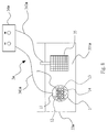
- FIG. 8 is a top view of another electroplating device for use in the method according to the present invention.
- FIG. 9 is a cross-sectional view of conventional semiconductor electrodes.
- the wafer 1 for use in a method for making semiconductor electrodes according to the preferred embodiment of the present invention.
- the wafer 1 includes at least one conductive unit 11 , a plurality of first connective units 12 connected to the conductive unit 11 , a plurality of first metal layers 13 connected to the first connective units 12 and a plurality of second connective units 14 connected to the first metal layers 13 .
- the first metal layers 13 may be made of gold-germanium alloy, gold-zinc alloy, gold-beryllium alloy or titanium-platinum-gold alloy.
- photo-resist 2 is provided on the first connective units 12 and the second connective units 14 while the first metal layers 13 are not covered with the photo-resist 2 .
- an electroplating device 3 is connected to the conductive unit 11 .
- Target material 331 is used in the electroplating device 3 .
- the target material 31 is gold, silver or gold-silver alloy.
- An electrode 32 of the electroplating device 3 is connected to the conductive unit 11 with a wire or probe.
- a second metal layer 4 is provided on each of the first metal layers 13 with the electroplating device 3 .
- the second metal layers 4 are made of gold, silver or gold-silver alloy corresponding to the target material 31 .
- a cutting step is conducted on the wafer 1 .
- the wafer 1 is cut through the photo-resist 2 .
- a semiconductor electrode is provided in the cutting step.
- the first connective units 12 and the second connective units 14 are used to ensure even current distribution so that the second metal layers 4 are made with uniform thickness. Therefore, there is no need to make the wafer 1 with a high carrier concentration.
- an electroplating device 3 a can be used instead of the electroplating device 3 .
- the electroplating device 3 a includes a container 33 a and a power supply 34 a .
- the container 33 a is used to contain electrolyte 331 a .
- the electrolyte 331 a includes gold, silver or gold-silver alloy.
- the power supply 34 a includes an electrode 341 a connected to the conductive unit 11 of the wafer 1 and an electrode 342 a connected to a mesh 35 .
- the mesh 35 is made of platinum alloy or titanium alloy. The wafer 1 and the mesh 35 are submerged in the electrolyte 331 a.
Landscapes
- Chemical & Material Sciences (AREA)
- Engineering & Computer Science (AREA)
- Chemical Kinetics & Catalysis (AREA)
- Electrochemistry (AREA)
- Materials Engineering (AREA)
- Metallurgy (AREA)
- Organic Chemistry (AREA)
- Life Sciences & Earth Sciences (AREA)
- Sustainable Development (AREA)
- Electroplating Methods And Accessories (AREA)
- Electrodes Of Semiconductors (AREA)
Abstract
Description
Claims (7)
Priority Applications (1)
| Application Number | Priority Date | Filing Date | Title |
|---|---|---|---|
| US12/081,946 US7928009B2 (en) | 2008-04-23 | 2008-04-23 | Method for making semiconductor electrodes |
Applications Claiming Priority (1)
| Application Number | Priority Date | Filing Date | Title |
|---|---|---|---|
| US12/081,946 US7928009B2 (en) | 2008-04-23 | 2008-04-23 | Method for making semiconductor electrodes |
Publications (2)
| Publication Number | Publication Date |
|---|---|
| US20100323515A1 US20100323515A1 (en) | 2010-12-23 |
| US7928009B2 true US7928009B2 (en) | 2011-04-19 |
Family
ID=43354710
Family Applications (1)
| Application Number | Title | Priority Date | Filing Date |
|---|---|---|---|
| US12/081,946 Expired - Fee Related US7928009B2 (en) | 2008-04-23 | 2008-04-23 | Method for making semiconductor electrodes |
Country Status (1)
| Country | Link |
|---|---|
| US (1) | US7928009B2 (en) |
Citations (2)
| Publication number | Priority date | Publication date | Assignee | Title |
|---|---|---|---|---|
| US20040065551A1 (en) * | 2002-05-07 | 2004-04-08 | University Of Southern California | Electrochemical deposition with enhanced uniform deposition capabilities and/or enhanced longevity of contact masks |
| US20040129573A1 (en) * | 2002-10-01 | 2004-07-08 | University Of Southern California | Multi-cell masks and methods and apparatus for using such masks to form three-dimensional structures |
-
2008
- 2008-04-23 US US12/081,946 patent/US7928009B2/en not_active Expired - Fee Related
Patent Citations (2)
| Publication number | Priority date | Publication date | Assignee | Title |
|---|---|---|---|---|
| US20040065551A1 (en) * | 2002-05-07 | 2004-04-08 | University Of Southern California | Electrochemical deposition with enhanced uniform deposition capabilities and/or enhanced longevity of contact masks |
| US20040129573A1 (en) * | 2002-10-01 | 2004-07-08 | University Of Southern California | Multi-cell masks and methods and apparatus for using such masks to form three-dimensional structures |
Also Published As
| Publication number | Publication date |
|---|---|
| US20100323515A1 (en) | 2010-12-23 |
Similar Documents
| Publication | Publication Date | Title |
|---|---|---|
| US8299477B2 (en) | Light emitting device and method for fabricating the same | |
| DE112015005964B4 (en) | Component and method for producing a component | |
| TWI353662B (en) | Lead cutter device | |
| US12224232B2 (en) | Semiconductor package having side wall plating | |
| CN107210581B (en) | Method for producing diode lasers and diode lasers | |
| US12211704B2 (en) | Semiconductor package having side wall plating | |
| CN102473717A (en) | Radiation-emitting semiconductor component | |
| BR9612562A (en) | Electrolytic process for cleaning electrically conductive surfaces. | |
| JP6392681B2 (en) | Anode unit and plating apparatus provided with the anode unit | |
| KR101832234B1 (en) | Leds using pec biasing technique and method for fabricating the same | |
| JP2015201634A (en) | Manufacturing method of mid circuit carrier, and mid circuit carrier | |
| DE102017200452B4 (en) | Method of manufacturing a semiconductor device | |
| US7928009B2 (en) | Method for making semiconductor electrodes | |
| CN101026211A (en) | Conductive support substrate through-hole vertical structure semiconductor chip or device | |
| US20110017604A1 (en) | Method for making semiconductor electrodes | |
| US10680369B2 (en) | Electrical connector contacts plated with an electrophoretic deposition coating and a precious-metal-alloy coating | |
| JPH07288340A (en) | Light emitting element and manufacture thereof | |
| KR20240131130A (en) | Separator plate for polymer electrolyte membrane water electrolyzer and polymer electrolyte membrane water electrolyzer stack | |
| TWI257723B (en) | Vertical light-emitting diode and method for manufacturing the same | |
| US20190378896A1 (en) | Diode comprising a semiconductor body | |
| KR101990129B1 (en) | Manufacturing method for Wire fixing type cylinder electrode | |
| US20080299756A1 (en) | Method and apparatus for plating a semiconductor package | |
| JP6070521B2 (en) | Manufacturing method of special shape electrodeposits | |
| JP3454283B2 (en) | Seawater battery | |
| KR102391643B1 (en) | Manufacturing method for thermoelectric module and thermoelectric module thereof |
Legal Events
| Date | Code | Title | Description |
|---|---|---|---|
| AS | Assignment |
Owner name: ATOMIC ENERGY COUNCIL-INSTITUTE OF NUCLEAR ENERGY Free format text: ASSIGNMENT OF ASSIGNORS INTEREST;ASSIGNORS:WU, CHIH-HUNG;LIU, KENG-SHEN;CHANG, CHUN-LING;AND OTHERS;REEL/FRAME:020891/0749 Effective date: 20080402 |
|
| STCF | Information on status: patent grant |
Free format text: PATENTED CASE |
|
| FPAY | Fee payment |
Year of fee payment: 4 |
|
| FEPP | Fee payment procedure |
Free format text: MAINTENANCE FEE REMINDER MAILED (ORIGINAL EVENT CODE: REM.); ENTITY STATUS OF PATENT OWNER: LARGE ENTITY |
|
| LAPS | Lapse for failure to pay maintenance fees |
Free format text: PATENT EXPIRED FOR FAILURE TO PAY MAINTENANCE FEES (ORIGINAL EVENT CODE: EXP.); ENTITY STATUS OF PATENT OWNER: LARGE ENTITY |
|
| STCH | Information on status: patent discontinuation |
Free format text: PATENT EXPIRED DUE TO NONPAYMENT OF MAINTENANCE FEES UNDER 37 CFR 1.362 |
|
| FP | Lapsed due to failure to pay maintenance fee |
Effective date: 20190419 |